CAUTION:
Before servicing this chassis, it is important that the service person read the "SAFETY PRECAUTIONS" and
"PRODUCT SAFETY NOTICE" contained in this manual.
MITSUBISHI DIGITAL ELECTRONICS AMERICA, INC.
9351 Jeronimo Road, Irvine, CA 92618-1904
Copyright © 2004 Mitsubishi Digital Electronics America, Inc.
All Rights Reserved
MITSUBISHIELECTRIC Ser
Ser
Ser
Ser
Service
vice
vice
vice
vice
Manual
Manual
Manual
Manual
Manual
2003
SET TOP BOX
V21S CHASSIS
SPECIFICATIONS
· Power Input
: AC 120V, 60Hz
· Power Usage
: 79W
· Frequency Range
: VHF
54 ~ 470MHz
UHF 470 ~ 806MHz
· Antenna Input
: VHF/UHF 75
unbalanced
2 - NTSC
1 -ATV/QAM
· Cabinet Weight and Demensions
· Input Level
: VIDEO IN JACK (RCA Type)
1.0Vp-p 75
unbalanced
: AUDIO IN JACK (RCA Type)
-4.7dBm 43k
unbalanced
: S-VIDEO IN JACK
(Y/C separate type)
Y:1.0 Vp-p C:0.286Vp-p(BURST)
75
unbalanced
: COMP / Y, Cr, Cb (RCA Type)
Y: 1.0 Vp-p Cr, Cb: 700mVp-p
: ATV / Y(G), Pr(R), Pb(B), H, V
Y: 1.0Vp-p with sync 75
(BNC)
Pr, Pb: 700mV 75
H, V: 3.0Vp-p 75
: VGA / R,G,B,V,H (15 pin D)
· Output Level
: VIDEO OUT JACK (RCA Type)
1.0Vp-p 75
unbalanced
: AUDIO OUT JACK (RCA Type)
-4.7dBm 4.7k
unbalanced
· Digital Interface
: IEEE-1394 I/O Jacks
: AC-3 Digital Audio Output
: MonitorLinkTM/DVI
: MonitorLinkTM Control/RS-232C
: NetCommand
®
.
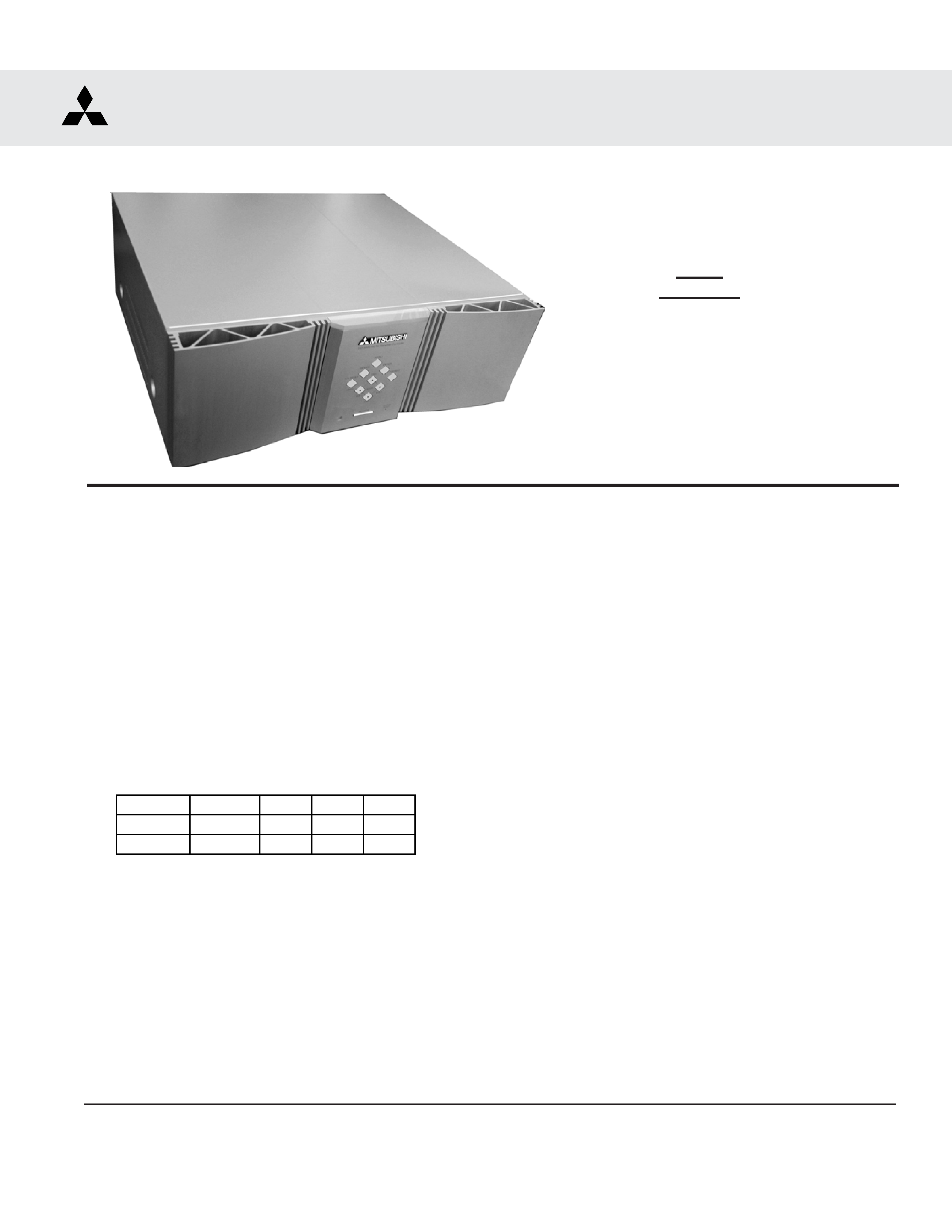
V21S
MODELS
HD-5000
HD-5000A
Mode l
W e ight
He ight W idth De pth
HD-5000
19 lbs.
8"
17"
16"
HD-5000A
19 lbs.
8"
17"
16"

MODELS: HD-5000 / HD-5000A
Page 3
INTRODUCTION ................................................................................................................................5
PRODUCT SAFETY NOTICE ............................................................................................................. 5
SAFETY PRECAUTIONS ................................................................................................................... 6
DISASSEMBLY
Top Cover Assembly / Disassembly ................................................................................................7
PCB Disassembly FlowChart .......................................................................................................... 7
PCB Assembly / Disassembly ........................................................................................................ 8
Cabinet Assembly / Disassembly ................................................................................................. 10
ELECTRICAL ADJUSTMENTS
Test Equipment ............................................................................................................................. 11
Initial Setup ................................................................................................................................... 12
LED Indicator Diagnostics ............................................................................................................. 13
Error Codes .................................................................................................................................. 13
Remote Control Operational Mode ................................................................................................ 13
Circuit Adjustment Mode ............................................................................................................... 14
On Screen Display Position Adjustment Mode .............................................................................. 15
Data Transfer Mode ....................................................................................................................... 15
E2PROM Replacement ................................................................................................................. 15
Adjustment Items List ................................................................................................................... 15
Adjustment Test Points ................................................................................................................. 17
Adjustment Procedures ................................................................................................................ 18
Audio Circuit ........................................................................................................................ 18
Character Position ............................................................................................................... 19
Main/Sub Y Level ................................................................................................................. 19
Color Alignment ................................................................................................................... 20
CHIP PARTS REPLACEMENT ......................................................................................................... 21
REPLACEMENT PARTS
Parts Ordering .............................................................................................................................. 22
Critical and Warranty Parts Designation ........................................................................................ 22
Parts Tolerance Codes .................................................................................................................. 22
Service Parts List .......................................................................................................................... 23
CIRCUITRY BLOCK DIAGRAMS
Standby Supplies Regulator .......................................................................................................... 32
DM Power Supply ......................................................................................................................... 33
Video / Color A/V Switch Circuit .................................................................................................... 34
Video / Color Signal Path .............................................................................................................. 35
Control Circuitry ............................................................................................................................ 36
Sound Circuitry ............................................................................................................................. 37
Sync Circuitry ............................................................................................................................... 38
CONTENTS

MODELS: HD-5000 / HD-5000A
Page 4
Section 2 .... Schematic Diagrams
SCHEMATIC DIAGRAMS
Overall Block Diagram ..................................................................................................................... 1
PCB-POWER / CONTROL / E2P .................................................................................................... 2
PCB-TERMINAL-1 [JACK] .............................................................................................................. 3
PCB-TERMINAL-2-1 [SWITCH] ....................................................................................................... 4
PCB-TERMINAL-2-2 [3DYC] ........................................................................................................... 5
PCB-SIGNAL-1 [MICRO] ................................................................................................................. 6
PCB-SIGNAL-2 [AV / IO] ................................................................................................................. 7
PCB-SIGNAL-3 [VIDEO / CHROMA] ............................................................................................... 8
PCB-SIGNAL-4 [IR / MV / DMP] ..................................................................................................... 9
PCB-2HDW-1 [IN] ......................................................................................................................... 10
PCB-2HDW-2 [MAIN] .................................................................................................................... 11
PCB-2HDW-3 [OUT] ..................................................................................................................... 12
PCB-2HDW-4 [C720] HD-5000A ONLY ......................................................................................... 13
PCB-DEMOD ................................................................................................................................14
PCB LAYOUT DIAGRAMS ............................................................................................................... 15
Page 5
MODELS: HD-5000 / HD-5000A
INTRODUCTION
This service manual provides service instructions for the V21S STB chassis type. The specific models for each
chassis type are listed below. Service personnel should read this manual thoroughly before servicing these chassis.
This service manual includes:
1. Saftey Precautions
2. Assembly and disassembly instructions.
3. Servicing printed circuit boards (PCBs).
4. Electrical adjustments.
5. Chip parts replacement procedures.
6. Circuit path diagrams.
The parts list section of this service manual includes:
1. Mechanical and Cosmetic parts.
2. Electrical parts.
Schematic and block diagrams of the above listed models are included in this service manual for better under-
standing of the circuitry. PCB drawings are also included for easy location of parts and test points.
PRODUCT SAFETY NOTICE
Many electrical and mechanical parts in television receivers have special safety related characteristics. These
characteristics are often not evident from visual inspection nor can the protection afforded by them necessarily be
obtained by using replacement components rated for higher voltage, wattage, etc.
Replacement parts which have special safety characteristics are identified in this service manual.
Electrical components having such features are identified by shading
on the schematic diagram and by bold
type in the parts list of this service manual. The replacement for any safety part should be identical in value
and characteristics.
V21S Cha ssis
HD-5000
HD-5000A
Page 6
MODELS: HD-5000 / HD-5000A
SAFETY PRECAUTIONS
NOTICE:
Observe all cautions and safety related notes located inside the receiver cabinet and on the
receiver chassis.
WARNING:
1.
Operation of this receiver outside the cabinet or with the cover removed presents a shock hazard
from the receiver's power supplies. Work on the receiver should not be attempted by anyone who is
not thoroughly familiar with the precautions necessary when working on high voltage equipment.
2.
When service is required, observe the original lead dress. Extra precaution should be taken to
assure correct lead dress in the high voltage area. Where a short-circuit has occurred, replace those
components that indicate evidence of overheating.
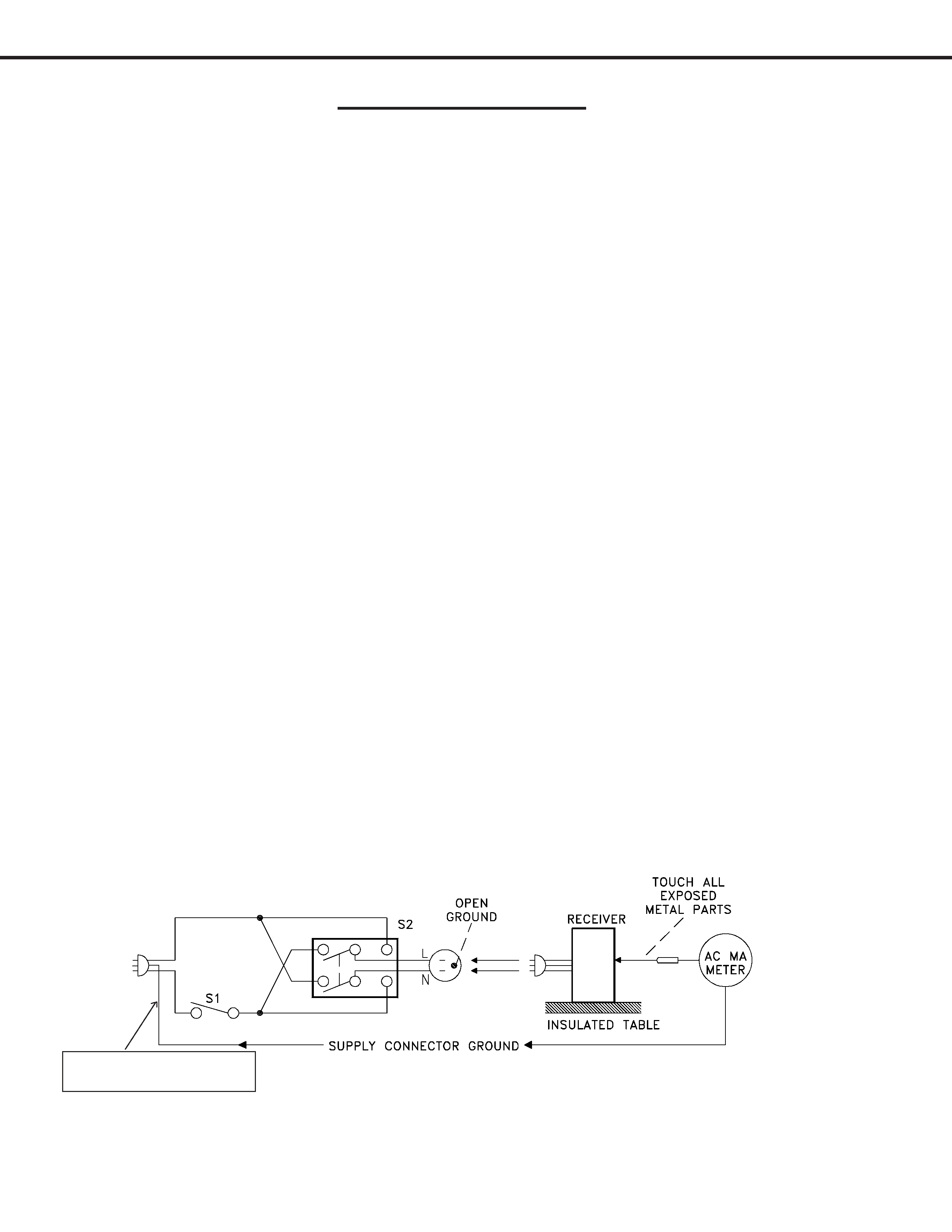
Leakage current check
Before returning the receiver to the customer, it is recommended that leakage current be measured according to
the following methods.
1. Cold Check
With the alternating current (AC) plug removed from the AC source, place a jumper across the two AC plug
prongs. Connect one lead of an ohm meter to the AC plug and touch the other lead to each exposed metal
part (i.e. antennas, handle bracket, metal cabinet, screw heads, metal overlay, control shafts, etc.), particu-
larly any exposed metal part that has a return path to the chassis. The resistance of the exposed metal parts
having a return path to the chassis should be a minimum of 1Mega Ohm. Any resistance below this value
indicates an abnormal condition and requires corrective action.
2. Hot Check ...Use the circuit shown below to perform the hot check test.
1. Keep switch S1 open and connect the receiver to the measuring circuit. Immediately after
connection, and with the switching devices of the receiver in their operating positions, measure
the leakage current for both positions of switch S2.
2. Close switch S1, energizing the receiver. Immediately after closing switch S1, and with the
switching devices of the receiver in their operating positions, measure the leakage current for both
positions of switch S2. Repeat the current measurements of items 1 and 2 after the receiver has
reached thermal stabilization. The leakage current must not exceed 0.5 milliampere (mA).
GWG - Green Wire Ground
(Earth Ground)