© 2001-12 PRINTED IN JAPAN
B51-7867-00 (N) 3417
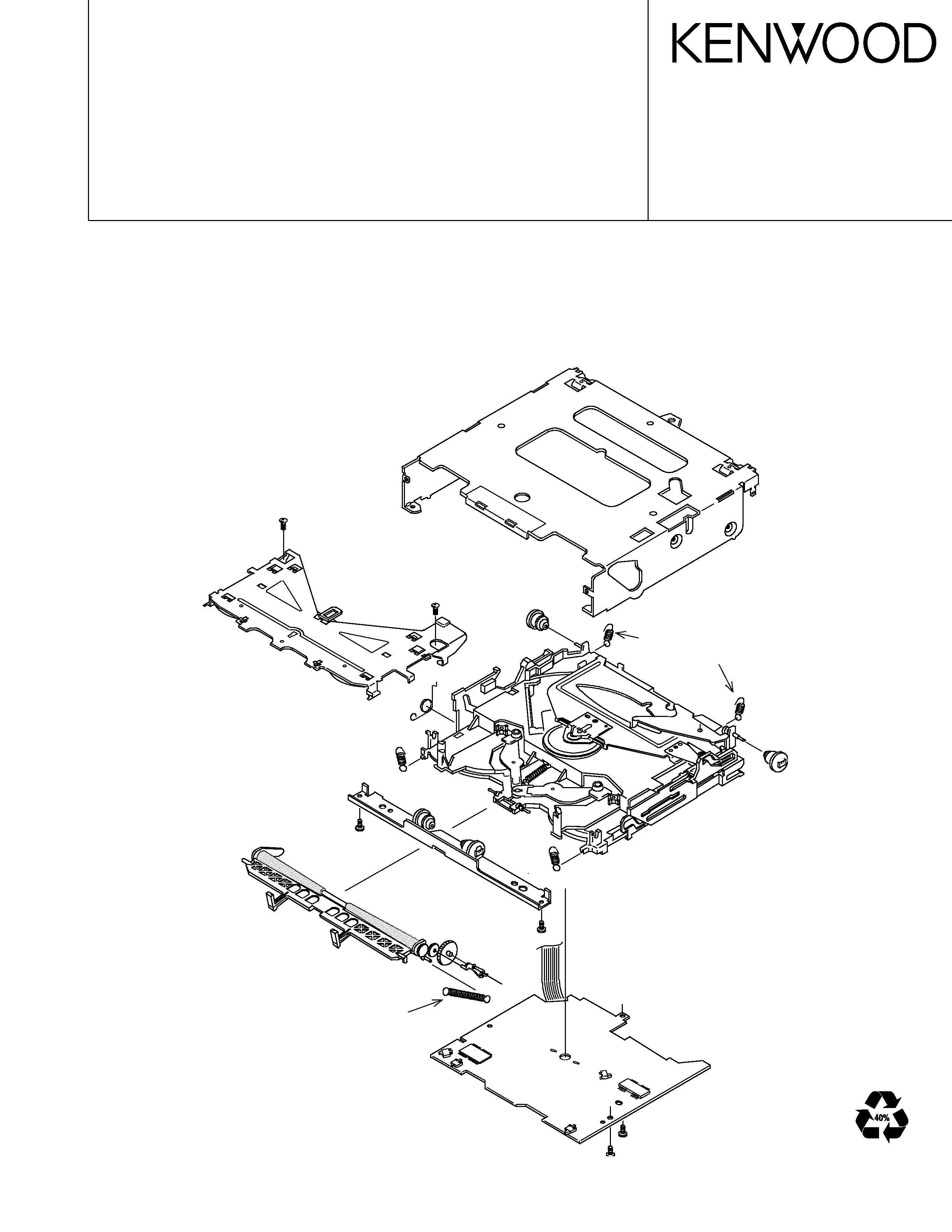
CD MECHANISM ASSY
SERVICE MANUAL
X92-4030-0x
X92-4440-0x
DESCRIPTION MECHANISM
X92-4030-00 (DXM-6000W)
X92-4030-01 (DXM-6001W)
X92-4030-02 (DXM-6002W)
X92-4030-03 (DXM-6003W)
X92-4030-04 (DXM-6004W)
X92-4030-05 (DXM-6005W)
X92-4440-00 (DXM-6100W)
X92-4440-01 (DXM-6101W)
X92-4440-02 (DXM-6102W)
X92-4440-03 (DXM-6103W)
X92-4440-04 (DXM-6104W)
X92-4440-05 (DXM-6105W)
outer-chassis
dumper (X4)
floating spring (X4)
traverse chassis assy
Mecha PCB
roller spring
roller lever assy
damper bracket
disc guide assy
CONSTRUCTION OF MAJOR PARTS
2
X92-4030-0x
X92-4440-0x
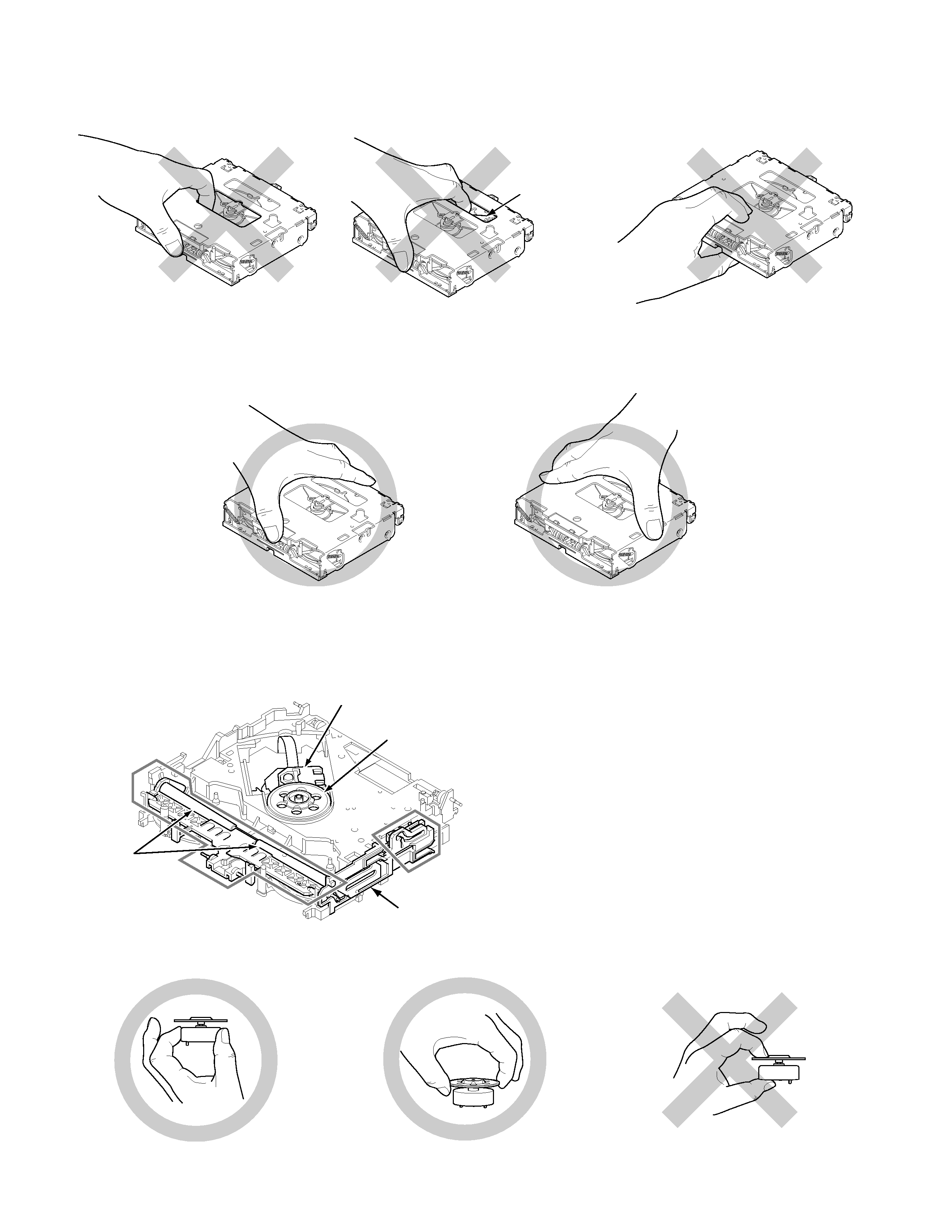
NOTE FOR HANDLING MECHANISM ASSY
Trigger Lever
Pick is under the finger, it
may touch.
NG
Don't touch the lever be-
cause the trigger lever
comes off.
NG
Don't have the center of
entrance because the disc
insertion mouth is trans-
formed.
NG
OK
OK
PICK UP
SPINDLE MOTOR
SLIDER ASSY
ROLLER
OK
OK
NG
· Don't touch in the frame, since grease is
applied to the parts.
· Don't applied grease to the roller.
· Don't touched PICK and SPINDLE MOTOR.
X92-4030-0x
X92-4440-0x
3
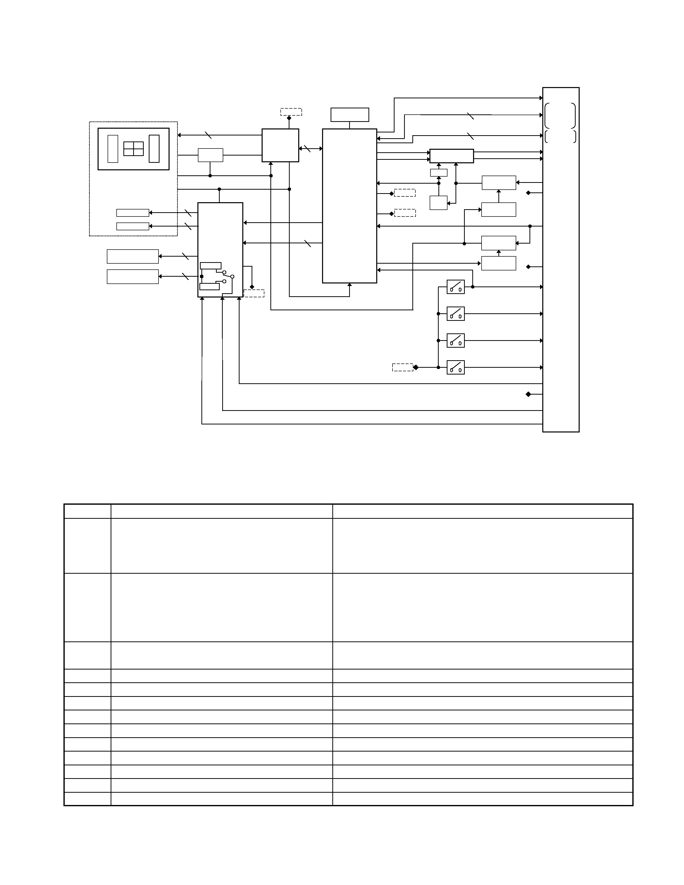
Mother Board
DOUT
22
X1
/CLK
19
D.GND
4
DATA
18
Pick-Up
/MSTOP
10
IC1
IC2
/MRST
11
5
2
/MUTE L
12
/MUTE R
13
AB
Q1
11
IC6
CD
L-ch
8
Vref
R-ch
6
Ref
Q3
A+5V
A.+8V
9
A.GND
A.GND
7
IC4
5V
Q2
2
Vref
Reg
D.GND
2
MUTE
DRVMUTE
Bu.+5V
15
Q4
7
2
Q5
Loding H
D.GND
14
2
Sled
L
Loe/Lim SW 1
S.GND
0-01Only
8Eje SW 17
12Eje SW 21
D.GND
Los SW
20
S7.5V
3
S.GND
2
Motor
4
Lo/Ej
5
RF Amp
Fo Coil
Servo Processor
+
MI-Com
1Chip IC
EF
APC
Tr Coil
S1
8V SW
Spindle Motor
Loading & Sled
Motor
Motor Driver
Vref
D2
SW
5V SW
SW
S3
S4
SW +5V
S2
Clock
16.93MHz
LPF
BLOCK DIAGRAM
COMPONENTS DESCRIPTION
Ref.No.
Application/Function
Operation/Condition/Compatibility
IC1
CD-RW compatible RF amplifier
Generation of RF and servo error (focusing error, tracking error)
signals based on the signals read from the APC circuit and
pickup, detection of dropouts, anti-shock, track crossing and off-
track signals, and gain switching for CD-RW.
IC2
CD signal processor LSI + Mechanism u-COM
Focusing, tracking, sled and spindle servo processing, automated
processing (focusing, tracking, gain, offset and balance), digital
signal processing (DSP, PLL, subcode, CIRC error correction and
audio data interpolation),
Text function (MN662773kH2), and microcomputer function.
IC4
4-CH BTL driver
Drive of the focusing coil, tracking coil, sled motor and spindle
motor, plus loading and ejection operations.
IC6
Audio active filter
Secondary LPF
Q1
For APC (Auto Power Control)
LD drive.
Q2
Q3 SW
ON when P-ON = "H" (when SW +5 V is ON).
Q3
A.8V SW
ON when P-ON = "H" (when Q2 is ON).
Q4
D.5V SW
ON when P-ON = "H" (when Q5 is ON).
Q5
Q4 SW(P-ON)
ON when P-ON = "H".
D1
Pickup laser diode protection
D2
D/A converter power supply diode
A.8V
A.5V
D3
For static protection
D4
For forced gain boost (tracking servo)
qCD PLAYER UNIT (X32-5170-0x/X32-5190-0x)
*
P-ON: Pin 82 of IC2.
X92-4030-0x
X92-4440-0x
4
MICROCOMPUTER'S TERMINAL DESCRIPTION
qMechanism Microcomputer (IC2 : X32-5170-0x, X32-5190-0x)
Pin No.
Name.
I/O
Description
Processing Operation
1
BDO
I
Dropout signal input. H: Detected.
Photodetector signal input 1.
2
OFT
I
Off-track signal input. H: Detected.
Photodetector signal input 2.
3
/RFDET
I
RF detection signal input. H: Detected.
Photodetector signal input 3.
4
VDET
I
Vibration detection signal input. H: Detected.
Photodetector signal input 4.
5
LDON
O
Laser diode ON signal output. H: ON.
Photodetector RF signal add input.
6
NC
-
No connection.
RF amp filter terminal 1.
7
NC
-
No connection.
RF amp filter terminal 2.
8
AVSS3
I
Analog circuit GND.
9
AVDD3
I
Analog circuit power supply.
10
FBAL
O
Focusing balance adjustment output.
Laser diode monitor input.
11
TBAL
O
Tracking balance adjustment output.
Laser diode drive output.
12
FE
I
Focusing error signal input (D/A input).
13
NC
-
No connection.
Tracking filter terminal 1.
14
NC
-
No connection.
Tracking filter terminal 1.
15
TE
I
Tracking error signal input (analog input).
16
NC
-
No connection.
Track cross comparator filter terminal.
17
NC
-
No connection.
18
NC
-
No connection.
RF signal input (for RF detection).
19
RFENV
I
RF envelope signal input.
20
VREF
I
VREF input.
21
ARF
I
RF signal input (for DSL).
22
DRF
I
DSL bias terminal.
23
DSLF
I/O
DSL loop filter terminal.
24
IREF
I
Reference current input.
25
PLLF
I/O
PLL loop filter terminal.
26
PLLF2
I/O
PLL loop filter characteristic switching terminal.
27
VCOF
I/O
VCO loop filter terminal.
28
VCOF2
I/O
Digital servo 33.8688 MHz generation (VCO loop filter terminal).
29
TRV
O
Traverse forced feed output.
30
TVD
O
Traverse drive output.
31
PC
O
Spindle motor ON output. L: ON.
32
ECM
O
Spindle motor drive output (forced mode output) (D/A output).
33
ECS
O
Spindle motor drive output (servo error signal output).
34
KICK
O
Kick pulse output.
35
TRD
O
Tracking drive output.
36
FOD
O
Focusing drive output.
37
TOFS
O
Tracking offset adjustment output.
38
AVDD2
I
Analog circuit power supply (for DSL, PLL, AD and DA circuits).
39
AVSS2
I
Analog circuit GND.
40
DVSS2
I
Digital circuit GND.
41
EFM or CK384
O
EFM signal output.
When command is executed:
16.9344 MHz clock output.
42
PCK or DSLB
O
PLL sampling clock output.
When command is executed:
DSL balance output.
43
/CLDCK
O
Subcode frame clock signal output.
44
FCLK
O
X'tal frame clock signal output.
45
IPFLAG
O
Interpolation flag signal output. H: Interpolated.
46
FLAG
O
Flag signal output.
47
TRCRS
I
Track crossing signal input.
Track crossing signal output.
48
STOUT
O
Serial data output for monitor signal (OFT, VDET, BDO, RFDET, etc.)
49
STLD
O
Load signal output for monitor signal.
50
SMCK
O
Bit clock signal output for monitor signal.
5
X92-4030-0x
X92-4440-0x
MICROCOMPUTER'S TERMINAL DESCRIPTION
Pin No.
Name.
I/O
Description
Processing Operation
51
CSEL
I
X'tal oscillation frequency selection terminal, which is fixed at L.
H: 33.8688 MHz. L: 16.9344 MHz.
52
TEST1
I
Test pin 1. Fixed at L (normal position).
53
TEST2
I
Test pin 2. Fixed at L (normal position).
54
IOSEL
I
Audio DAC external data input mode selection terminal.
55
/NRST
I
Reset input. L: Reset.
56
BCLK
O
SRDATA bit clock output.
57
LRCK
O
L/R identification signal output.
58
SRDATA
O
Serial data output.
59
SUBC
O
Subcode serial output.
60
SBCK
I
Subcode serial output clock input.
61
DQSY
O
CD-TEXT read permission signal output.
62
DEMPH
O
De-emphasis detection signal output. H: ON.
63
TX
O
Digital audio interface signal output.
64
SRDATAIN
I
SRDATA input/test terminal.
65
LRCKIN
I
LRCK input/SMCK output frequency switching.
66
BCLKIN
I
BCLK input. When not used: VDD.
67
DVDD1
I
Digital circuit power supply.
68
X1
I
X'tal oscillator input terminal.
69
X2
O
X'tal oscillator output terminal.
70
DVSS1
I
Digital circuit GND.
71
XSUB1
I
Microcomputer clock input terminal.
72
XSUB2
O
Microcomputer clock output terminal.
73
DVDD2
I
Digital circuit power supply.
74
NC
O
No connection.
75
NC
O
No connection.
76
73/74SEL
I
73/74 selection port.
77
DRV_MUTE
O
Driver muting control terminal.
78
NC
O
No connection.
79
NC
O
No connection.
80
TEST
I
Test mode switching terminal.
81
ASEL
I
Audio output polarity detection terminal.
82
PON
O
Audio/digital power supply control terminal.
83
SEARCH
O
Servo IC gain switching control terminal.
84
EQCNT
O
RF amp double-speed switching control terminal.
85
SW3
I
Limit switch detection terminal.
86
/MUTE_L
O
L-CH analog muting control terminal.
87
/MUTE_R
O
R-CH analog muting control terminal.
88
CD_RW
O
CD-RW control terminal.
89
/RST
I
System reset input terminal.
90
MECHASEL
I
6000/6010 selection port.
L=6000 H=6010
91
/MSTOP
I
Standby detection terminal.
92
LDCNT
O
LD control terminal.
93
DATA
I/O
I2C bus data line (communication line with System controller).
94
/CLK
I/O
I2C bus clock data line (communication line with System controller).
95
HOT
I
Temperature protection detection terminal.
96
VREF+
I
A/D converter + power supply.
97
OUTR
O
R-channel audio output.
98
AVDD1
I
Analog circuit power supply (for audio output circuits of
both L and R channels).
99
OUTL
O
L-channel audio output.
100
AVSS1
I
Analog circuit GND (for audio output circuits of both L
and R channels).