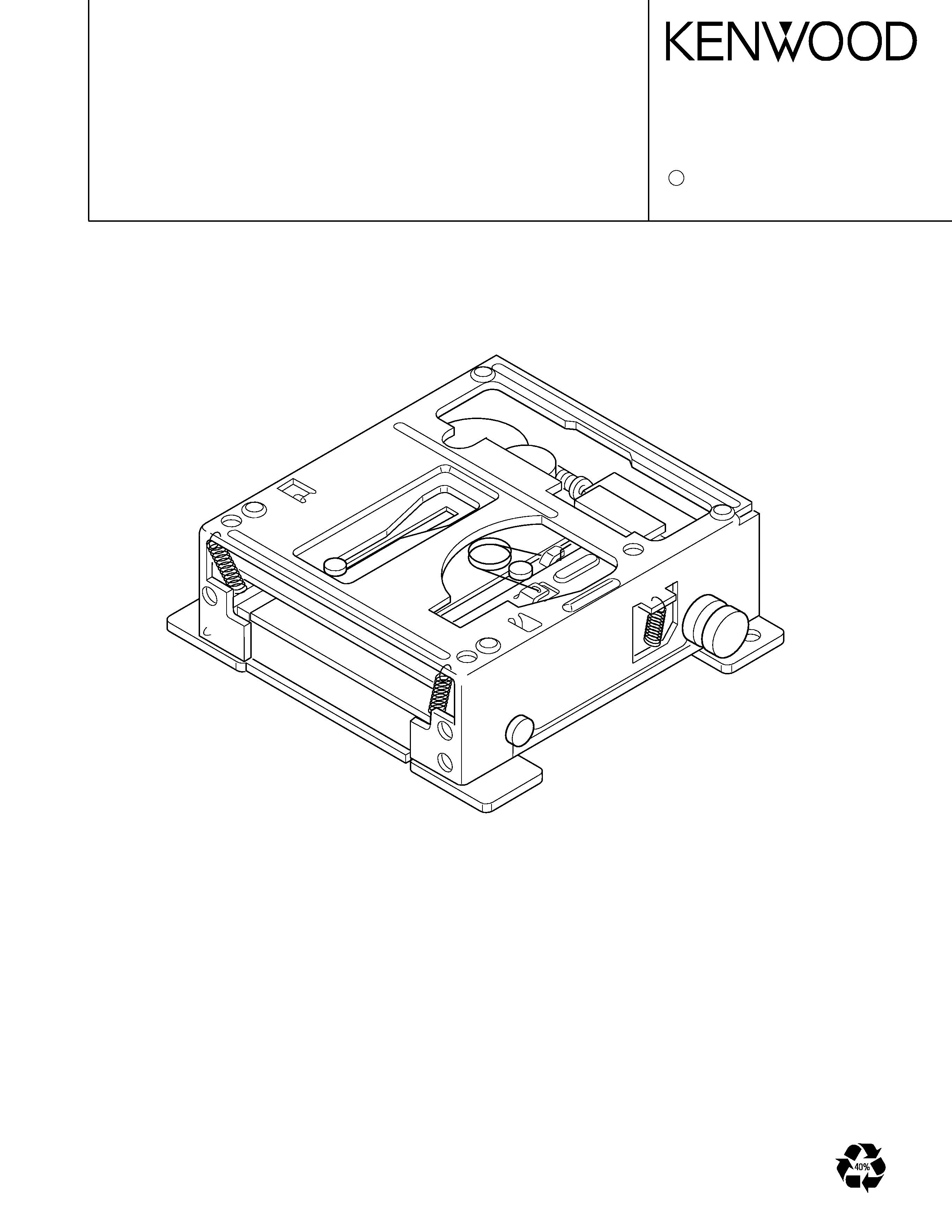
MD MECHANISM ASSY
X92-3770-00,0-01
X92-3780-00,0-01
2000-5 PRINTED IN JAPAN
B51-7623-00 (4) 3360
SERVICE MANUAL
C
CONTENTS
BLOCK DIAGRAM .............................................................. 2
COMPONENT DESCRIPTION ........................................... 3
MICROCOMPUTER'S TERMINAL DESCRIPTION ........... 3
ADJUSTMENT .................................................................... 5
MECHANISM OPERATION DESCRIPTION ..................... 7
PC BOARD ....................................................................... 24
EXPLODED VIEW ............................................................ 26
SCHEMATIC DIAGRAM ................................................... 27
PARTS LIST ..................................................................... 29
2
1
2
4
5
6
7
8
9
3
15
14
I
J
A
B
C
D
E
F
11
12
22
23
25
41
42
19
APC
APCREF
EQADJ
3TADJ
WBLADJ
FZC
RF
AUX1
AUX2
PEAK
BOTT
OM
ABCD
FE
VC
SWDT
SCLK
XLA
T
FOCONT
109
108
103
104
101
100
107
106
SPFD
SPRD
FFDR
FRDR
TFDR
TRDR
SFDR
SRDR
11
14
11
9
6
13
12
MNT0
MNT1
MNT2
MNT3
XINT
SQSY
SENS
SRDT
SCLK
SWDT
XLA
T
XRST
36
38
39
14
57
59
58
23
22
FZC
XINT
SQSY
SENS
SRDT
SCLK
SWDT
XLA
T
XRST
28
32
17
27
26
62
64
37
35
61
3
LDON
SDMUTE
LIMITSW
P-ON
AMUTE
MSDA
MSCL
MSTOP
MRST
TYPE1
TYPE2
15
10
11
12
13
16
47
29
30
MNT
4
MNT
3
MNT
2
MNT
1
MNT
0
4M/16M
HOT
ESDA
ESCL
20
19
17
16
29
30
23
22
26
25
24
32
33
TRK+
TRK-
FCS+
FCS-
SLED+
SLED-
SPDL+
SPDL-
VC
VREF0
VCC2
VCC1
LOAD
EJECT
10
11
12
13
6
7
8
9
28
27
3
14
5
TFDR
TRDR
FFDR
FRDR
SFDR
SRDR
SPFD
SPRD
REG
IN
REG
OUT
ENREG
LOAD
EJECT
11
10
8
13
12
19
18
14
17
4
5
1
20
21
6
7
A8V
L-CH
R-CH
MRST
MST
OP
MSCL
(IIC
BUS)
MSDA
AMUTE
BU5V
S5V
S5V
LOE-SW
LOS-SW
DET
-SW
LOAD
EJECT
36
30
29
31
34
35
37
33
38
47
46
48
40
10
28
26
32
17
18
20
27
16
42
41
MORF
RFO
AUX
1
FOCONT
XSTBY
ADFG
22.58MHz
11
8
11
7
11
6
19
7
5
4
2
1
3
73
74
75
76
70
81
90
77
78
79
80
93
97
96
95
94
82
89
88
1
13
11
5
9
10
8
12
2
6
8.38MHz
4
MUTE1
MUTE2
1
2
MUTE3
36
CH1,2
CH3
CH4
31
57
SW+5V
DA
VDD
AUDIO
+B
JITTER
RECORD
IN
VC
TE
SE
VC
VC
VC
VC
PD
LD
STBY
T
O
CH5
OP
S+B
SW+5V
S5V
+3.3V
BU+5V
6
5
BU+5V
1.2V
rms
1KHz
0dB
SW+5V
T
O
SER
VO
DRIVER
BU+5V
ILCC
LDON
RF
AMP
RF
AGC
&
EQ
RF
AMP
CXA2523AR
BPF
P-P
PEAK
&
BOTT
OM
ABCD
AMP
IV
AMP
IV
AMP
CVB
AMP
TEMP
VICCONV
ERROR
AMP
FOCUS
AT
AMP
BPF
TRACKING
ERROR
AMP
SERIAL
P
ARALLEL
DECODER
BALANCE
E-F
FILTER
PLL
DECODER
ACIRC
EFM
MEMOR
Y
RESIST
ANT
SHOCK
CONTROLLER
DYNAMIC
RAM
A
TRAC
DECODER
DIGIT
AL
FIL
TER
CONVER
TER
D/A
POST
FIL
TER
CONTROL
MONIT
OR
ANALOG
MUX
ADIP
DEMODULA
T
O
R
DECODER
SPINDLE
SER
VO
GENERA
T
O
R
PWM
APC
DSP
SER
VO
CONVER
TER
A/D
CLOCK
GENERA
T
O
R
AUT
O
SEQUENCER
I/F
CPU
PROCESSOR
SUBCODE
TC74HCT7007AF
MECHA
u-COM
UPD78015FYGC
CH2
DRIVER
CH1
DRIVER
DRIVER
CH4
DRIVER
CH3
VREF
DRIVER
CH5
NJM4565MD
LPF
SW+8V
A3.3V
REG.
LIMIT
SW
LOE-SW
LOS-SW
DET
-SW
A
TRAC
DECODER
DET
.
REFLECT
APC
CB
DA
F
E
J
I
DETECT
OR
TRACKING
COIL
FOCUS
COIL
M
SLED
MOT
OR
SPINDLE
MOT
OR
M
LOADING/EJECT
MOT
OR
M
THERMISTER
EEPROM
S-24C01B
128
8BIT
SW+5V
EFM/ACIRC
DECODER
SHOCK
PROOF
MEMOR
Y
CONTROLLER
DIGIT
AL
SER
VO
PROCESSOR
DIGIT
AL
SIGNAL
PROCESSOR
1M-WORD
4BIT
DYNAMIC
RAM
DIGIT
AL
FIL
TER.
D/A
CONVER
TER
CDX2659R
FOCUS/TRACKING
COIL
DRIVER
SPINDLE/SLED
MOT
OR
DRIVER
LA6552
LOADING/EJECT
MOT
OR
DRIVER
IC1
Q1
IC4
Q3
IC2
IC1
1
IC9
IC5
IC8
Q10
IC12
Q13
Q7
MOT
O
R
ASS'Y
KMS-242B
OPTICAL
PICKUP
BLOCK
MOT
OR
BLOCK
X33
UNIT
X92-3770-00,0-01/X92-3780-00,0-01
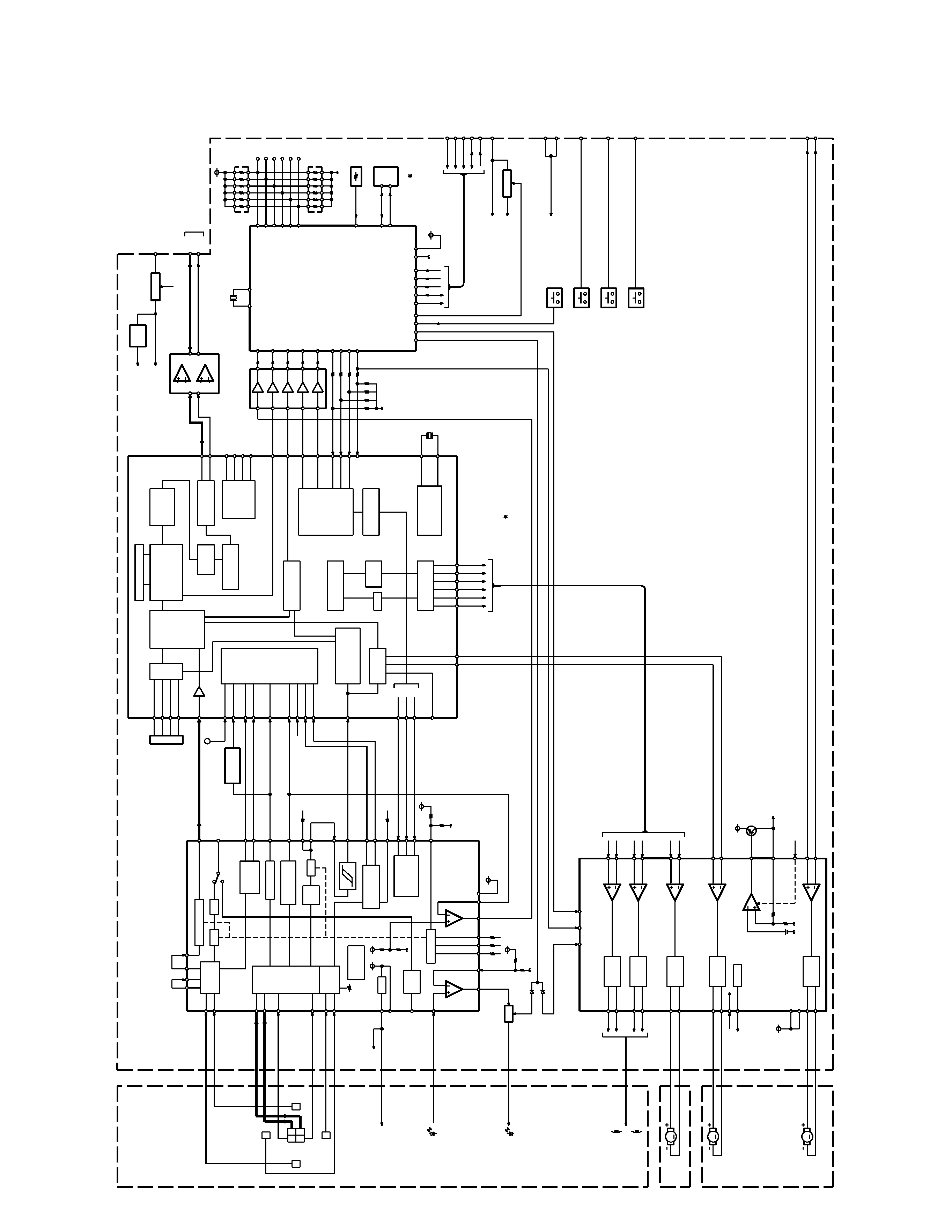
BLOCK DIAGRAM

MICROCOMPUTER'S TERMINAL DESCRIPTION
3
X92-3770-00,0-01/X92-3780-00,0-01
COMPONENT DESCRIPTION
IC1
IC2
IC4
IC5
IC8
IC9
IC11
IC12
Q1
Q2
Q3
Q7
Q10
Q12
Q13
CXA2523AR
CXD2659R
LA6552
NJM4565MD
LP2982-3.3
TC74HCT7007AF
78015FYGC-R08
S-24C01B
2SA1362(Y)
DTA114EUA
2SC4116(Y)
MCH6101
2SA1576A
DTC143EUA
2SA1576A
RF matrix amp.
Digital signal processor
5ch BTL driver
LPF
3.3V AVR
CMOS buffer
MD mechanism MI-COM.
E2PROM
APC
LD SW
Disc reflection detection
3.3V AVR
A 8VSW
P ON 5V SW
RF amplifier (pit and groove switching, AGC, EQ), gain switching
I-V amplifier.
Amplification of the light intensity signal output, peak hold output,
bottom hold output, FE output, TE output, SE output, ADIP binary
output, VREF output and APC PD
EFM decording, EFM digital PLL, ACIRC decording, auto link pro-
cessing, ADIP decording.
Digital servos (focusing, tracking, sled, spindle CLV).
ATRAC decording, 1bit D/A, analog post-filtering, memory control.
Drives actuators and motors, +3.3V REGULATOR
Third active filter
D/A audio +B
Level shifting from 3.3V to 5.0V
Servo control, memory control, system control and interfacing
Servo coefficients and servo adjustment data backup memory
Laser power control.
On at base"L" while laser is OFF.
On when focusing point is passed during upward search.
Servo +B
Analog 8V power supply.
On at base"L"
Ref. No. Component Name
Application/Function
Operation/Condition/Compatibility
MD PLAYER UNIT (X33-3040-00/0-01)
1
2
3
4
5
6
7
8
9
10
11
12
13
14
15
16
17
18
19
20
21
22
23
24
25
"H" turns normal test mode ON.
"L": 200ms, "H": 300ms
"L": 2655R, 2652AR, "H": 2655BR, 2654R
"H" turns special test mode ON.
"H" turns external input mode ON.
75% or more remains at "H"
IVR-TBAL auto align bus at "H"
AGC auto align bus at "H"
Error count mode at "H"(When it's in text mode)
Reverse polarity at "H".
"H" turns 16M bit operation (fixed on RESET)
"L" when innermost limit is detected.
During 2652AR : ON at "H", during 2654R : ON at "L"
Active : "L"
Latch at falling edge
Test mode input 0
Groove area jump time selection input
Destination selector 2
Test mode input 3
E2PROM external input test mode
Test mode memory remainder output
OPEN
OPEN
No auto align mode input
No auto align mode input
C1 error count mode input
GND
Internal status input from DSP LSI
DAC output polarity reversal input
DRAM size selection input
Pickup innermost limit detection
OPEN
OPEN
OPEN
De-emphasis output to external DAC
Reset output to DSP LSI and servo driver IC
Latch output to DSP LSI
OPEN
Pin No.
Microprocessor : 78015FYGC-R08 (X33 : IC11)
Description
Processing Operation
I
I
I
I
I
O
O
O
I
I
I
I
I
I
I
I
O
O
O
O
O
O
O
I/O
TEST0
JTIME
TYPE2
TEST3
TESTE
M REM
NC
NC
VSS
IVRTBAL PASS
AGC PASS
C1 COUNT
NC
SENS
AUDIO INV
4M/16M
LIMSW
NC
NC
NC
DEEM
XRST
XLAT
VSS
NC
Pin Name

4
X92-3770-00,0-01/X92-3780-00,0-01
MICROCOMPUTER'S TERMINAL DESCRIPTION
Pin No.
Description
Processing Operation
I/O
Pin Name
26
27
28
29
30
31
32
33
34
35
36
37
38
39
40
41
42
43
44
45
46
47
48
49
50
51
52
53
54
55
56
57
58
59
60
61
62
63
64
Active : "L"
Active : "L"
Active : "H"
(I2C-BUS)
(I2C-BUS)
Active : "L"
Active : "L"
"H"for interrupt request generation
Active : "L"
"L"for interrupt status generation
Vth On : 3.87V, Vth Off : 3.74V, Vth Low : 0.43V
Jitter input during FBAL alignment
"H"with AVREF reference voltage
"H"for manual adjustment mode
"L": 2655R, 2655BR, "H": 2652AR, 2654R
(I2C-BUS)
(I2C-BUS)
Audio mute output
Unit internal system power control output
Laser APC control output
E2PROM serial data line
E2PROM serial clock line
OPEN
Sled driver mute output
OPEN
OPEN
Reset input from system
µ-COM.
FZC interrupt request input
Standby control input from system
µ-COM.
Interrupt request from DSP LSI
Sub-code Q sync or ADIP sync input
Connect crystal oscillator as main system
clock.
Connect crystal oscillator as main system
clock.
(not used : BU5V connection)
Temperature detection input
AUX1 input durring 2654R mode/
others not used
OPEN
OPEN
OPEN
OPEN
OPEN
AVREF terminal control output
Connected to AVCON terminal
Serial data input from DSP LSI
Serial data output to DSP LSI
Shift clock output to DSP LSI
Manual adjustment mode input
Destination selector 1
Serial data line with system
µ-COM.
OPEN
Serial clock line with system
µ-COM.
O
O
O
I/O
I/O
O
O
O
O
I
I
I
I
I
I
I
I/O
O
O
O
O
O
O
I
O
O
I
I
I/O
O
I/O
AMUTE
P-ON
LDON
ESDA
ESCL
NC
SDMUTE
NC
NC
MRST
FZC
M-STOP
XINT
SQSY
VDD
X2
X1
IC
XT2
NC
AVSS
HOT
AUX1/NC
NC
NC
NC
NC
NC
AVCON
AVDD
AVREF
SRDT
SWDT
SCLK
LADJ1
TYPE1
MSDA
NC
MSCL

ADJUSTMENT
5
X92-3770-00,0-01/X92-3780-00,0-01
Service Test Mode (Manual Adjustment Mode) of the MDS-2200
The focusing bias (balance) adjustment of the MDS-2200 has been subjected to automatic adjustment at the factory and the
obtained bias value has been written in the E2PROM, and the set performs adjustment by reading the E2PROM data.
Consequently, after the pickup has been replaced in servicing, it is required to adjust the focusing bias again. This can be done
automatically if the dedicated commander for the MDS-2200 and a jitter meter are available, but the set also incorporates a
service test mode (manual adjustment mode) for use in case these instruments are not available.
· Adjustment procedure (Be sure to begin setup while the power of the set is off.)
1. Pull up pin 60 (LADJ1 (check land 1)) of lC11 in the X33-unit to BU5V (check land BU5).
2. Lead wires from check land ARF and check land SAG (servo GND) in the X33-unit so that they an be monitored with an
oscilloscope.
3. Turn the set on and perform the reset power-ON operation.
The adjustment includes three modes ; the Iow-reflection pit and groove modes for recordable discs and the high-reflection
pit mode for premastered discs.
4. Load a disc to enter the adjustment mode.
<With a recordable disc>
5. The low-reflection pit play mode starts when TNo.1 is displayed.
The time code display shows "50".
6. While monitoring ARF with an oscilloscope, vary the focusing bias using the Track UP and DOWN keys.
7. The optimum values can be obtained by varying the bias in the UP and DOWN directions, locating the upper and lower values
at which the ARF waveform is disturbed or the 3T waveform level drop, and calculating the center value of the two values.
For example, when the value located in the UP direction is 58 and that located in the DOWN direction is 46, the optimum value
is their center value, i. e. 52.
8. When the optimum value is obtained, set the focusing bias to that value and press the ManuaI UP or DOWN key to enter the
value.
(With normal sets, press and hold the Track UP or DOWN key.)
9. After the low-reflection pit adjustment in step 8, the pickup automatically moves to the groove area.
10. The groove play mode starts when TNo.2 is displayed.
11. Perform the same operations as steps 6, 7 and 8.
12. The disc stops after the groove area adjustment .
Eject the disc and complete adjustment.
Since the low-reflection pits are present only in the TOC area, their total play time is about 40 seconds. When the pit area
is over, the retry operation starts and the adjustment is invalid in this period.
<With a premastered disc>
13. When the high-reflection play mode starts, perform operations in steps 5, 6, 7 and 8.
14. The disc stops after the adjustment. Eject the disc and complete adjustment.
The coarse adjustment of the EF balance is also performed during this test mode.
However, it is an automatic adjustment and does not require external poeration.