© 2003-11 PRINTED IN JAPAN
B51-8669-00 (N) 1011
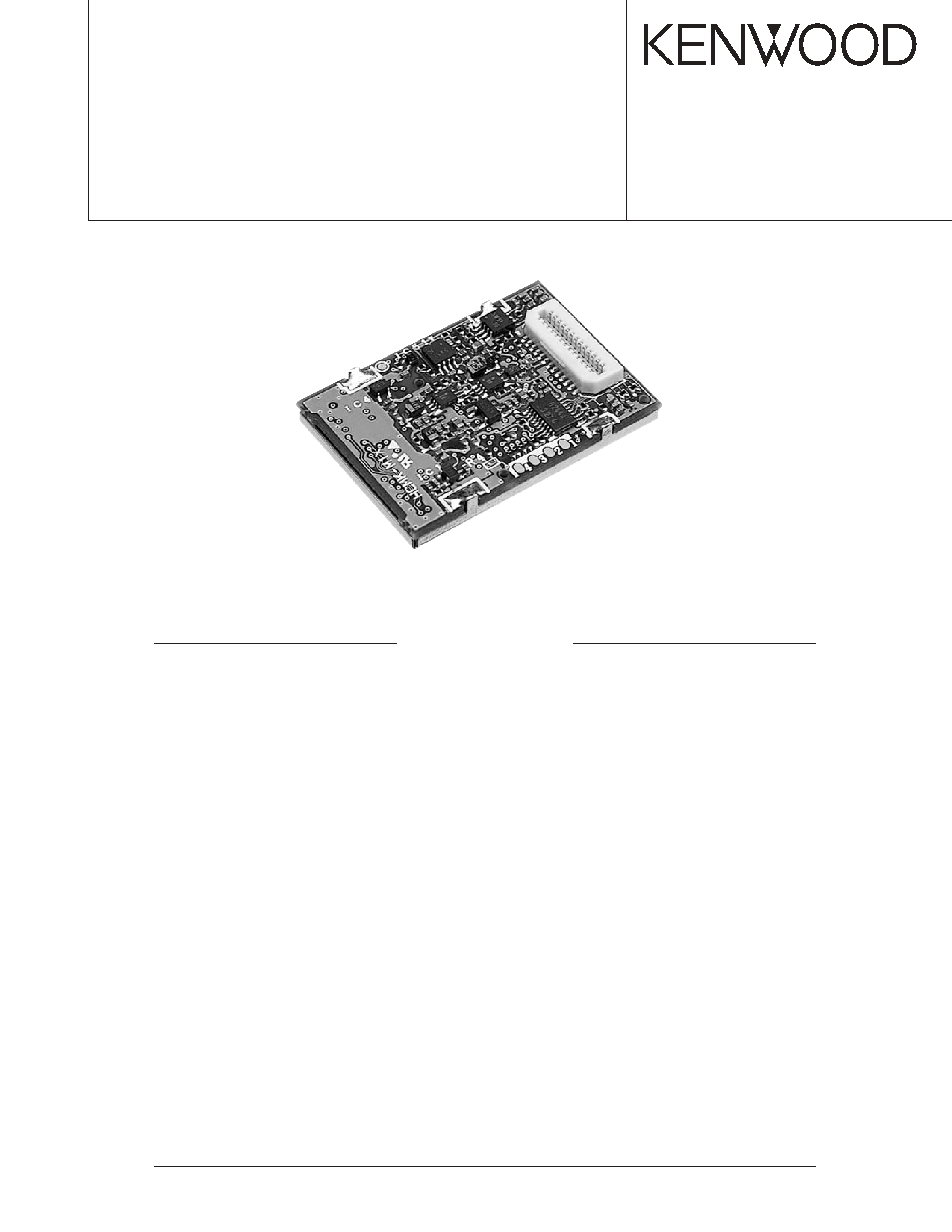
VOICE GUIDE & STORAGE UNIT
VGS-1
SERVICE MANUAL
CIRCUIT DESCRIPTION
Recording/Playback Operation .................................................................... 2
I/O Ports ......................................................................................................... 2
Beat Shift Circuit ........................................................................................... 3
Amateur Transceiver Identification ............................................................. 3
SEMICONDUCTOR DATA
MCU : HD6433024D01TE (IC2) ...................................................................... 4
Reset IC : S-80930CNNBG80 (IC1) ................................................................ 5
Analog Switch : TC7W66FK (IC53, IC54) ...................................................... 5
Bus Switch with Level Shifting : TC7MBD3244AFK (IC57) ........................ 5
COMPONENTS DESCRIPTION ......................................................................... 6
PARTS LIST ........................................................................................................ 6
PC BOARD
ACCESSORY UNIT (X42-3250-60) ................................................................ 8
SCHEMATIC DIAGRAM ..................................................................................... 9
TERMINAL FUNCTION .................................................................BACK COVER
CONTENTS
VGS-1
2
CIRCUIT DESCRIPTION
Recording/Playback Operation
Recording
The audio signal input from the AI pin (CN1 pin 12) passes
through a buffer amplifier (IC52 2/2) and goes to an anti-
aliasing filter amplifier (IC52 1/2).
The audio signal is amplified by approx. 30 times by IC52
1/2 and unwanted signal components exceeding 4kHz are
cut by an LPF.
The amplified audio signal is input to pin 78 of the MCU
(IC2 : Micro Controller Unit).
The MCU converts the audio signal to a digital data (by
8kHz/8-bit sampling) and writes it into a flash memory (IC3,
IC5).
When the input level of the AI pin is 100mVp-p, the MCU
input becomes approx. 3Vp-p, and the maximum S/N can be
achieved.
If a signal exceeding 100mVp-p is input to the AI pin, it is
clipped by IC52 so that the MCU input does not exceed 3Vp-
p to protect the MCU against over-voltage input.
Playback and Prerecorded Voice
The audio signal saved in flash memory (IC3, IC5) is con-
verted to an analog signal by the MCU (IC2) and output as a
playback signal from pin 84.
This playback signal passes through two LPFs to cut har-
monic components and is input to the attenuator circuit.
The attenuator circuit consists of analog switch ICs (IC53,
IC54) and division resistors (R64, R66, R67, R71, R72).
The signal attenuated by the attenuator circuit is con-
verted to a low impedance by an output buffer (IC55), then
output from the AO pin (CN1 pin 11).
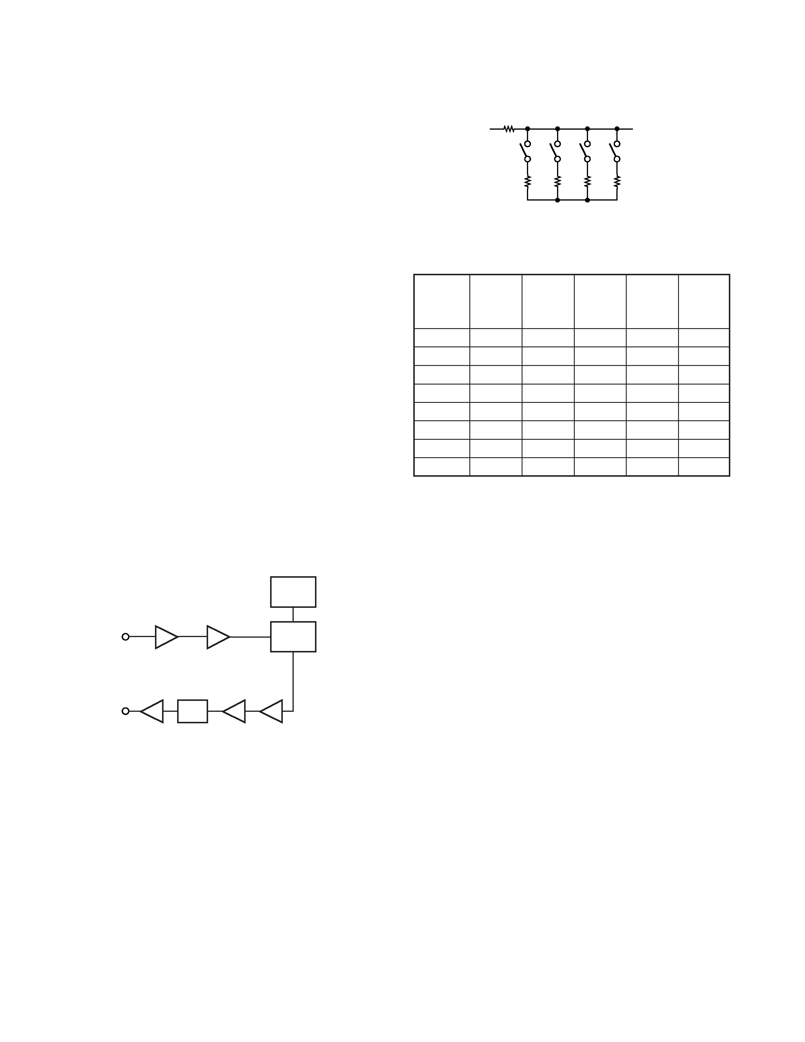
IC3, IC5
FLASH
IC2
MCU
+
+
+
+
IC53,IC54
ATT
IC55
Buffer
IC51
LPF
IC51
LPF
AO
AI
X1
X1
AN0
78
DA0
84
+
IC52
Buffer
IC52
LPF amp
X30
Fig. 1
Signal flow
Attenuator Circuit
An attenuator circuit with division resistors is built by con-
trolling four analog switches of IC53 and IC54 with pins 95 to
98 of the MCU (IC2).
The output level is changed in 8 steps with 4-bit data.
R66
R67
R71
R72
R64
IC53
IC54
Fig. 2
ATT circuit
Attenuator Circuit Control Table
95pin
96pin
97pin
98pin
PA2
PA3
PA4
PA5
ATT1
ATT2
ATT3
ATT4
Vol0
Lo
Lo
Lo
Lo
100%
Vol1
Hi
Lo
Lo
Lo
69%
Vol2
Lo
Hi
Lo
Lo
55%
Vol3
Hi
Hi
Lo
Lo
44%
Vol4
Lo
Lo
Hi
Lo
36%
Vol5
Lo
Hi
Hi
Lo
28%
Vol6
Lo
Lo
Lo
Hi
15%
Vol7
Lo
Lo
Hi
Hi
12%
I/O Ports
The VGS-1 is a 3V system unit, but it can be adapted to
both 3V and 5V systems for external connection devices with
an 8-bit CMOS bus switch (IC57).
IC57 can convert levels from 3V to 3V, from 3V to 5V, or
from 5V to 3V.
If the External Device is a 3V System
It can be connected without a pull-up resistor.
If the External Device is a 5V System
If the external connection device is a 5V system, the VGS-
1 output ports (BUSY, SO, PLAY) must to be pulled up to 5 V.
The waveform may become irregular due to IC57 output ca-
pacity and pull-up resistance.
BUSY and PLAY are Hi/Lo logic output ports and are not
much affected by pull-up resistance.
Even when 3V or 5V is input to an input port, the IC57
output is 3V.
· UART Control
For UART control, the maximum communication speed is
115200 bps, and SO pull-up resistor recommends approx
10k
.
· Synchronous Control
SO is not used for synchronous control.
Only PLAY and BUSY must to be pulled up.
VGS-1
3
CIRCUIT DESCRIPTION
O
O
I
I
IC57
VGS-1
External device
5V
5V
Pull-up
resistor
Pull-up
resistor
Fig. 3
External device, pull-up resistor
AI Input Port
If input exceeds 100mVp-p, the input signal is clipped and
distortion occurs.
It is necessary to make setting so that no signals exceed-
ing 100mVp-p are input.
If the input level lowers, S/N decreases, so the maximum
input not exceeding 100mVp-p must be used.
AO Output Port
When recording is performed with a 100mVp-p input, the
playback output becomes an approx. 2.8Vp-p level.
If Prerecorded Voice is generated, the output is approx
2Vp-p.
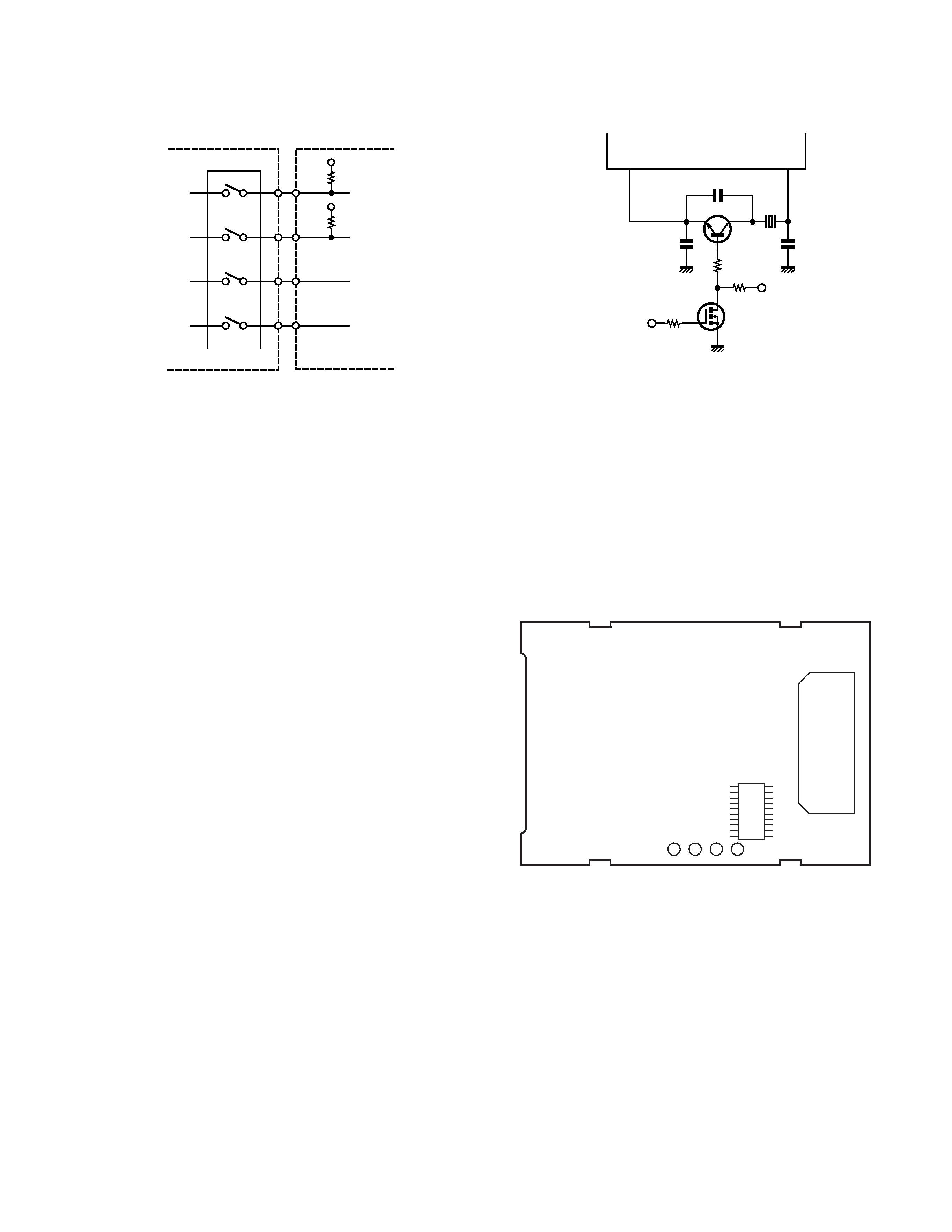
Beat Shift Circuit
To prevent VGS-1 clock oscillation for the MCU (IC2) from
causing spurious reception to transceivers to which VGS-1 is
connected, the clock oscillator (11.0592MHz) has a beat shift
circuit with a transistor switch (Q1).
Beat Shift Circuit Off
Pin 94 of the MCU (IC2) goes Low level, Q2 turns off, and
Q1 turns on because a 5V bias is applied to its base. In this
condition, C10 is shorted, so the oscillation frequency is un-
changed.
Beat Shift Circuit On
Pin 94 of the MCU goes High level, Q2 turns on, and Q1
turns off because its base is pulled down to GND. In this
condition, C10 is connected in series to the crystal oscillator
and the oscillation frequency increases by approx. 150ppm.
Fig. 4
Beat shift circuit
Amateur Transceiver Identification
The VGS-1 can be set as an amateur transceiver or a Land
Mobile Radio transceiver in the factory.
When it is used as a Land Mobile Radio transceiver, inter-
nal data in the VGS-1 is changed to suit the Land Mobile Ra-
dio transceiver, so it cannot be used as an amateur trans-
ceiver.
The VGS-1 set as a Land Mobile Radio transceiver can be
identified because the RV4 land on the PCB is at High level.
The default is Low level.
C10
X1
Q1
Q2
R19
R18
C11
C12
R17
5V
IC2 94 pin
PA1
High : Normal
Low : Shift
66
67
XTAL
EXTAL
IC2
MCU
RV1
RV2
RV3
RV4
Accessory unit
Foil side view
Fig. 5
RV4
VGS-1
4
SEMICONDUCTOR DATA
MCU : HD6433024D01TE (IC2)
Pin No.
Port Name
I/O
Function
Remarks
1
VCC1
I
3.3V
2
BUSY
O
Busy state output
Hi : BUSY
3
PLAY
O
Playback state output
Hi : PLAY
4~9
NC
O
Not used
10
FWE
O
Not used
Pull Down
11
VSS1
I
GND
12
NC
O
Not used
13
TXD1
O
Serial data output
14
RXD0
I
Not used
Pull Up
15
RXD1
I
Serial data input
16
NC
O
Not used
17
SCK1
I
Serial clock input
18~20
RV1~RV3
I/O
21
RV4
O
AMR correspondence output
Lo : For AMR
22
VSS2
I
GND
23
NC
O
Not used
24
USEL
I
UART bit rate selection
Lo : 19200bps, Hi : 115200bps
25
SELF
I
Transceiver connection selection
Lo : Transceiver connected
26
P47
I
Lo
27~34
D8~D15
I/O
Data bus
IC3 · IC5
35
VCC2
I
3.3V
36~43
A0~A7
O
Address bus
IC3 · IC5
44
VSS3
I
GND
45~56
A8~A19
O
Address bus
IC3 · IC5
57
VSS4
I
GND
58
_WAIT
I
Not used
Pull Up
59
_BREQ
I
Not used
Pull Up
60
NC
O
Not used
61
fai
O
For system clock frequency check
62
_STBY
I
Not used
Pull Up
63
RESET
I
Reset input
Lo : RESET
64
NMI
I
Not used
Pull Up
65
VSS5
I
GND
66
EXTAL
I
System clock input
11.0592 MHz
67
XTAL
I
System clock input
11.0592 MHz
68
VCC3
I
3.3V
69
NC
O
Not used
70
OE
O
SRAM/Flash memory read output
Lo : Read,
IC3 · IC5
71
WE
O
SRAM/Flash memory write output
Lo : Write,
IC3 · IC5
72
NC
O
Not used
73
MD0
I
Microcomputer operation mode input 0
Hi
74
MD1
I
Microcomputer operation mode input 1
Lo
75
MD2
I
Microcomputer operation mode input 2
Hi
76
AVCC
I
3.3V
Analog power supply
77
VREF
I
3.3V
Analog reference voltage
VGS-1
5
SEMICONDUCTOR DATA
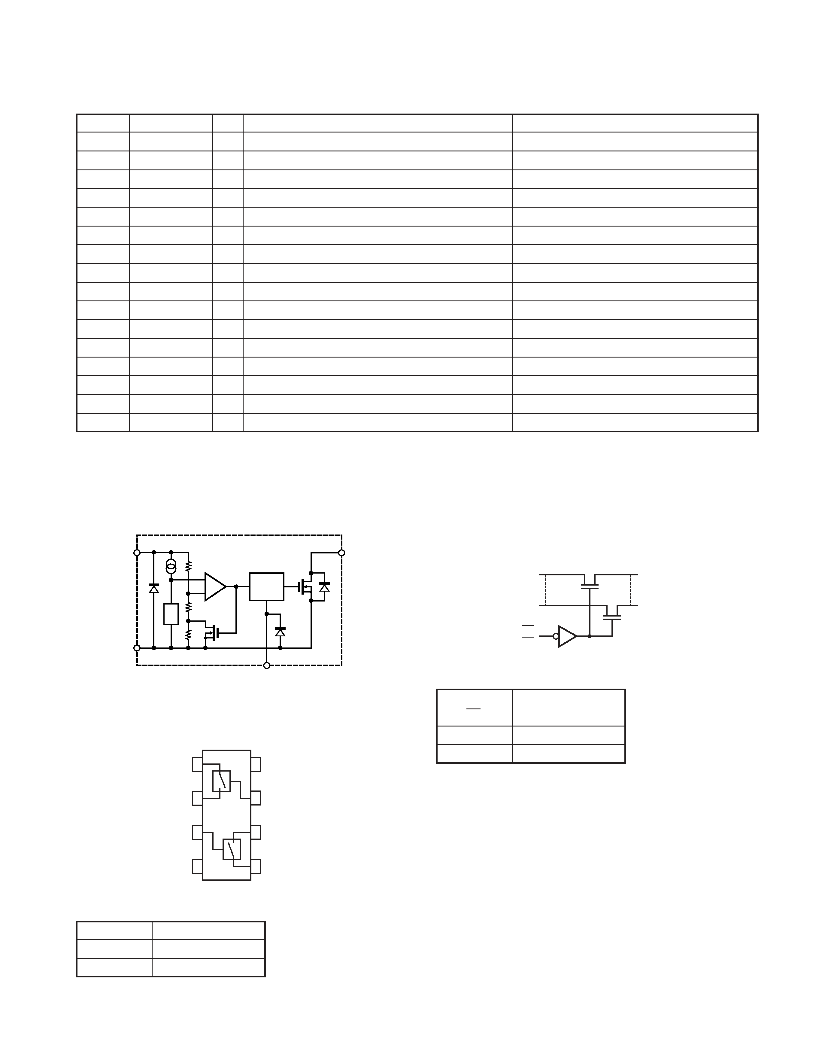
Reset IC : S-80930CNNBG80 (IC1)
Block Diagram
+
Delay
circuit
VDD
VSS
CD
OUT
V
ref
*
*
*
* : Parastic diode
Analog Switch : TC7W66FK (IC53, IC54)
Block Diagram
Truth Value Table
CONTROL
SWITCH FUNCTION
HON
LOFF
Bus Switch with Level Shifting
: TC7MBD3244AFK (IC57)
System Figure
Truth Value Table
Input
Function
OE
LA port = B port
H
Disconnect
18
7
6
5
2
3
4
IN/OUT1
IN/OUT2
OUT/IN1
OUT/IN2
CONT2
CONT1
GND
VCC
1OE
(2OE)
1A4
(2A4)
1A1
(2A1)
1B4
(2B4)
1B1
(2B1)
Pin No.
Port Name
I/O
Function
Remarks
78
AN0
I
A/D conversion (Voice input)
79~83
AN1~AN5
I
Not used
Pull Down
84
DA0
O
D/A conversion (Voice output)
85
NC
O
Not used
86
AVSS
I
GND
Analog GND
87
EN
I
Enable input/Power save relese interruption
Lo : Enable
88
_CS3
O
Chip select output (IC5)
Lo : Chip select
89
_CS2
O
Chip select output (IC3)
Lo : Chip select
90
_CS1
O
Chip select output (SRAM)
Lo : Chip select
91
NC
O
Not used
92
VSS6
I
GND
93
RD/_BY
I
Flash memory busy input
Lo : BUSY (Erasing / Writing),
IC3 · IC5
94
PA1
O
Beat shift control
Hi : ON
95~98
ATT1~ATT4
O
Voice output attenuation control
Hi : ON
99
AFM
O
Voice output mute control
Hi : ON
100
A20
O
Address bus
IC3 · IC5