© 2003-11 PRINTED IN JAPAN
B51-8667-00 (N) 694
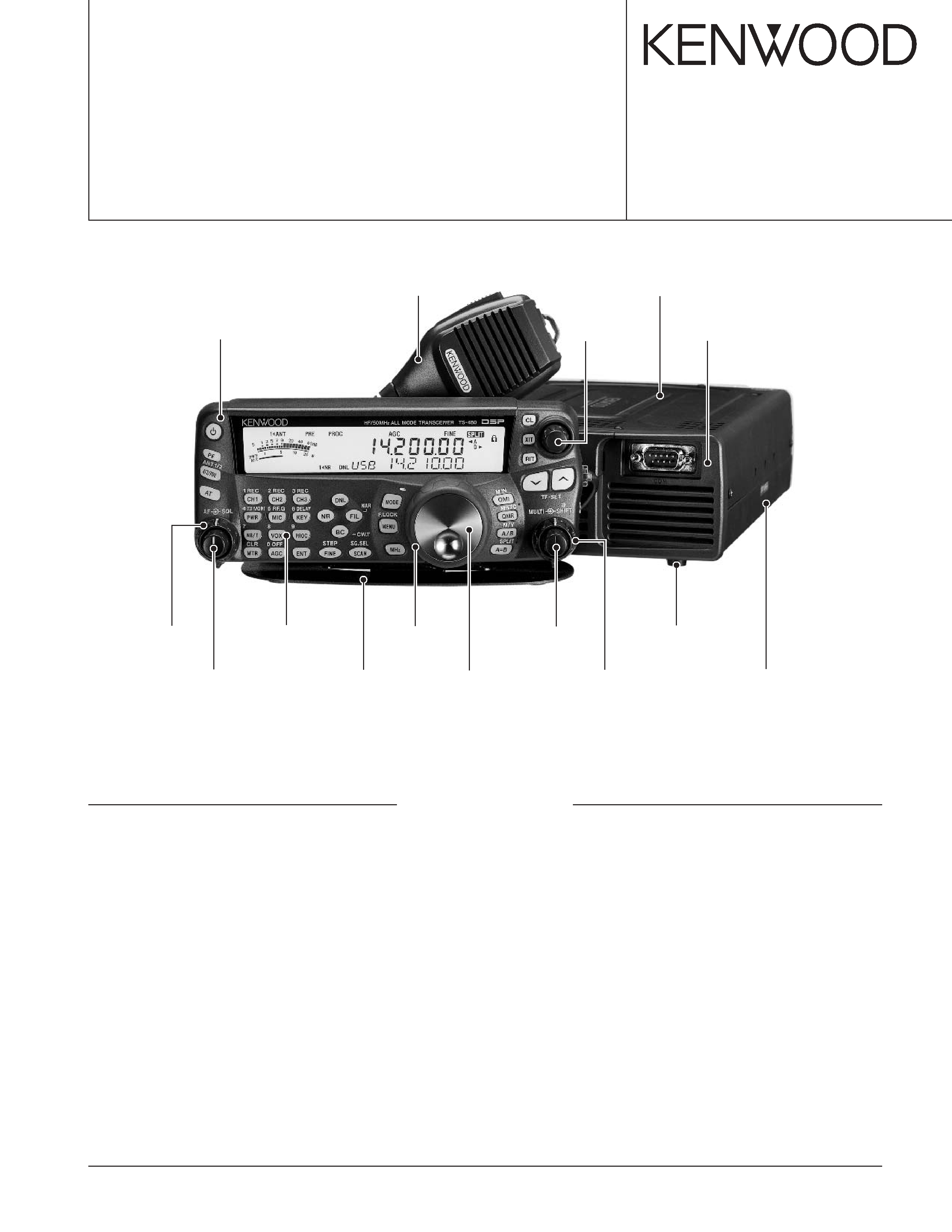
HF / 50MHz ALL MODE TRANSCEIVER
TS-480HX/480SAT
SERVICE MANUAL
DISASSEMBLY FOR REPAIR .................................. 2
CIRCUIT DESCRIPTION ........................................... 3
COMPONENTS DESCRIPTION ............................. 14
SEMICONDUCTOR DATA ..................................... 20
PARTS LIST ............................................................ 27
EXPLODED VIEW ................................................... 50
PACKING ................................................................ 54
ADJUSTMENT ....................................................... 55
INTERCONNECTION DIAGRAM ........................... 76
PC BOARD / SCHEMATIC DIAGRAM
RF UNIT (X44-327X-XX) .................................... 78
FINAL UNIT (X45-365X-XX) (A/3) ..................... 86
FINAL UNIT (X45-365X-XX) (B/3) ..................... 93
FINAL UNIT (X45-365X-XX) (C/3) ..................... 96
FINAL UNIT (X45-366X-XX) (A/3) ..................... 98
FINAL UNIT (X45-366X-XX) (B/3) ................... 105
FINAL UNIT (X45-366X-XX) (C/3) ................... 108
DISPLAY UNIT (X54-3410-00) (A/3, B/3, C/3) ....... 110
TX-RX UNIT (X57-663X-XX) (A/2, B/2) .......... 116
SUB UNIT (X58-4900-XX) ................................ 128
TERMINAL FUNCTION ........................................ 129
BLOCK DIAGRAM ................................................ 134
LEVEL DIAGRAM ................................................. 136
ACCESSORIES ..................................................... 140
SPECIFICATIONS ................................................. 141
Knob
(K29-9270-03)
Knob (Main dial)
(K21-1105-03)
Knob ring
(K29-9264-04)
Knob
(K29-9266-03)
Knob
(K29-9267-03)
Cabinet (Lower)
(A01-2190-02)
Knob
(K29-9265-03)
Knob
(K29-9267-03)
Panel assy
(A62-1076-03)
Key top
(K29-9263-02)
Stand
(J09-0409-03)
Microphone
(T91-0638-05)
Cabinet (Upper)
(A01-2189-02)
Panel
(A62-1079-01)
Foot
(J02-0441-05) x 4
CONTENTS
TS-480HX/480SAT
2
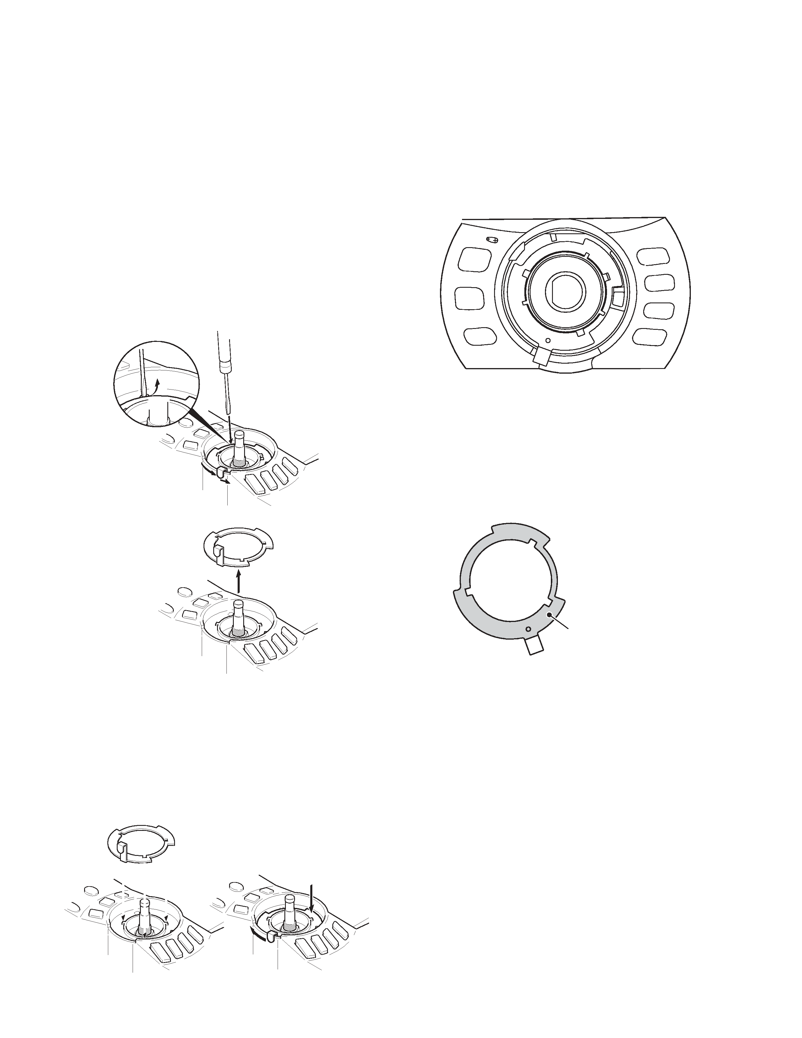
How to remove the torque changeover le-
ver (G02-0898-04)
1. Turn the lever section of the torque changeover lever to
the right. ( q )
2. Insert the tip of a flat-head screwdriver into the recessed
part of the torque changeover lever. ( w )
3. Lift the torque changeover lever using the tip of the flat-
head screwdriver. ( e )
Caution: Be careful not to damage the torque changeover
lever when lifting it.
4. Turn the lever section of the torque changeover lever to
the right, as in the position described in step 3. ( r )
5. Lift the torque changeover lever and remove it from the
panel ASSY.
DISASSEMBLY FOR REPAIR
q
w
e
r
How to mount the torque changeover le-
ver (G02-0898-04)
1. Insert the torque changeover lever into the mounting loca-
tion so that the three tabs align with the torque
changeover slots. (Fig.1)
2. Turn the lever section of the torque changeover lever to
the left while pressing the surface of the lever as shown in
the Fig. 2, and mount it onto the panel ASSY.
Apply the dry-surf 2400
onto the front and rear
surfaces of the torque
changeover lever.
Fig. 1
Fig. 2
Cautions for mounting the main dial knob
(K21-1105-03)
Confirm that the lever section of the torque changeover
lever is in the fully turned left position (Torque OFF) before
mounting the main dial knob.
Cautions for replacing the torque change-
over lever
Apply the dry-surf 2400 onto the front and rear surfaces
after replacing the torque changeover lever. (Do not apply the
dry surf to the lever section.)
TS-480HX/480SAT
3
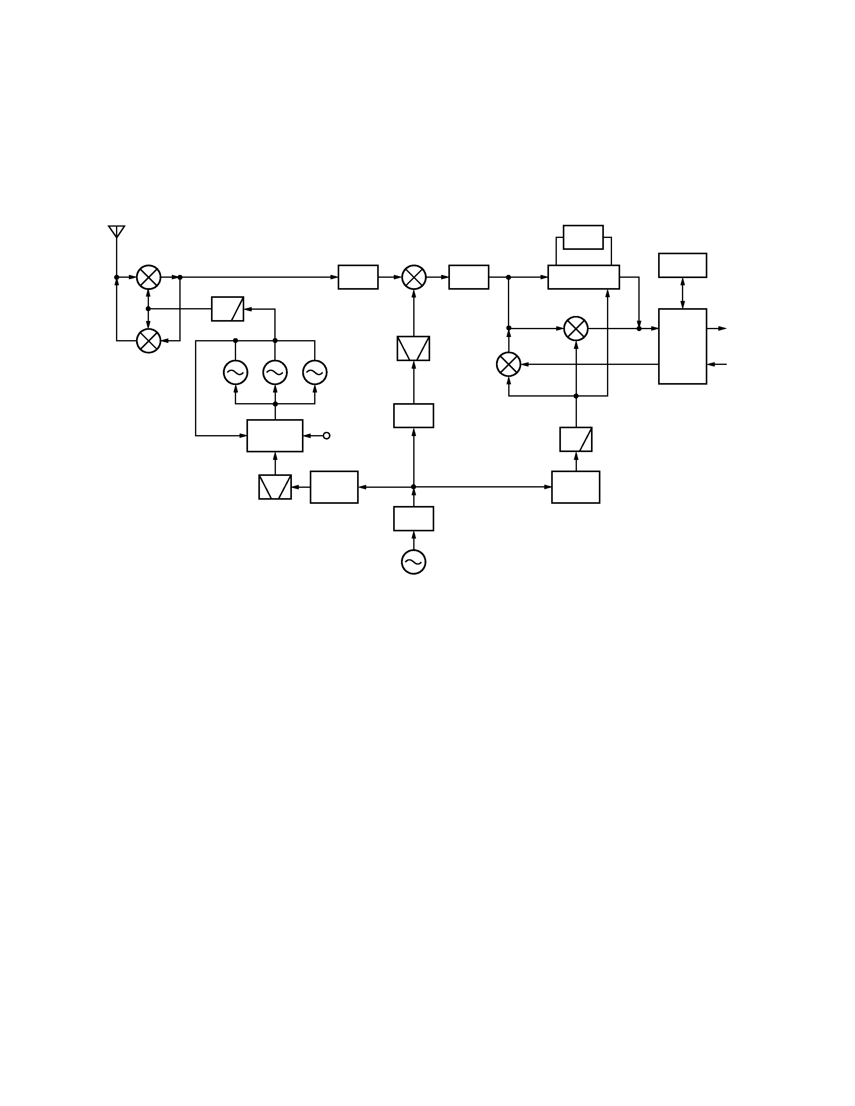
Frequency Configuration
Figure. 1 shows the frequency configuration of this trans-
ceiver. All modes operate in a double conversion while trans-
mitting. FM mode operates in a triple conversion and other
modes operate in a double conversion while receiving.
CIRCUIT DESCRIPTION
PLL
LMX2360
VCO1 VCO2
VCO3
73.125~
133.095MHz
CF1
PLL REF
8.33~
8.47MHz
DDS
AD9835
DDS
AD9835
DDS REF
DDS REF
73.095MHz
1st IF
10.695MHz
2nd IF
3rd IF
LO1
RX MIX
TX MIX
TX/RX
MIX
LO2
62.4MHz
x2
x2
Except
FM
RX MIX
TX
MIX
455kHz
FM IC
FM
CODEC
31.2MHz
fstd
X1
15.6MHz
10.695MHz (Except FM)
10.24MHz (FM)
CAR
CAR
DSP
AF OUT
MIC IN
FM MOD
ANT
Fig. 1
Frequency configuration
Reference Signal Generator
The reference frequency (fstd), which is used to control
the PLL frequency, oscillates at 15.6MHz in a crystal oscilla-
tion circuit (X1, Q1). This 15.6MHz signal passes through a
buffer amplifier (Q4) and is doubled in a multiplier (Q5) to gen-
erate a 31.2 MHz signal. The 31.2MHz signal is used as the
reference signal for the DDS (IC1) for the PLL reference sig-
nal of the first local oscillator (LO1) and the DDS (IC2) for a
carrier (CAR).
The SO-3 (TCXO unit) is configured as an option in this
transceiver, so that you can replace the crystal oscillation cir-
cuit (X1, Q1) with the SO-3. However, you must cut the R103
(0
) and R104 (0) jumper wires to stop the operation of the
crystal oscillation circuit (X1, Q1) when using the SO-3.
LO1/LO2/CAR
LO1 (the 1st local oscillator)
A frequency between 8.33MHz and 8.47MHz is output
using the 31.2MHz signal as the reference signal in the DDS
(IC1). The output signal passes through a ceramic filter (CF1)
and enters into a PLL (IC3). This signal is divided into 1/8 (1/
R) in the PLL and becomes the comparison frequency fø for
the frequency between 1.041MHz and 1.058MHz.
The VCOs (Q451, Q452, Q456) of LO1 oscillate between
73.125MHz and 133.095MHz. The oscillation output of
these VCOs enter pin 6 of the PLL (IC3), then divides into 1/N
in the PLL. The comparison frequency fø is compared with
the frequency divided into 1/N by a phase comparator in the
PLL, then locks the frequency to use it as the output fre-
quency of LO1.
In the DDS (IC1), the output frequency (8.33MHz to
8.47MHz) is swept with fDDS STEP [Hz]=10 x R/N when the
step is 10Hz or fDDS STEP [Hz]=1 x R/N when the step is 1Hz.
Therefore, LO1 covers the frequency range of 73.125MHz to
133.095MHz with 10Hz or 1Hz steps.
The PLL output generated by the above-mentioned
method is amplified at Q15 and passes through a band-pass
filter with a cutoff switching circuit, an attenuator, and a low-
pass filter, and is then sent to the RF unit (X44-327) as LO1.
LO2 (the 2nd local oscillator)
The 15.6MHz (reference frequency) signal passes through
a buffer amplifier (Q4) and is doubled in a multiplier (Q5) to
generate a 31.2MHz signal. The resistance of the 31.2MHz
signal is distributed since it is used as the reference signal for
each DDS (IC1, IC2). The 31.2MHz signal is doubled in a
multipler (Q8, Q12) to generate a 62.4MHz signal.
The band-pass filter cuts the high harmonic of the
62.4MHz signal and the signal is sent to the RF unit (X44-327)
as LO2.
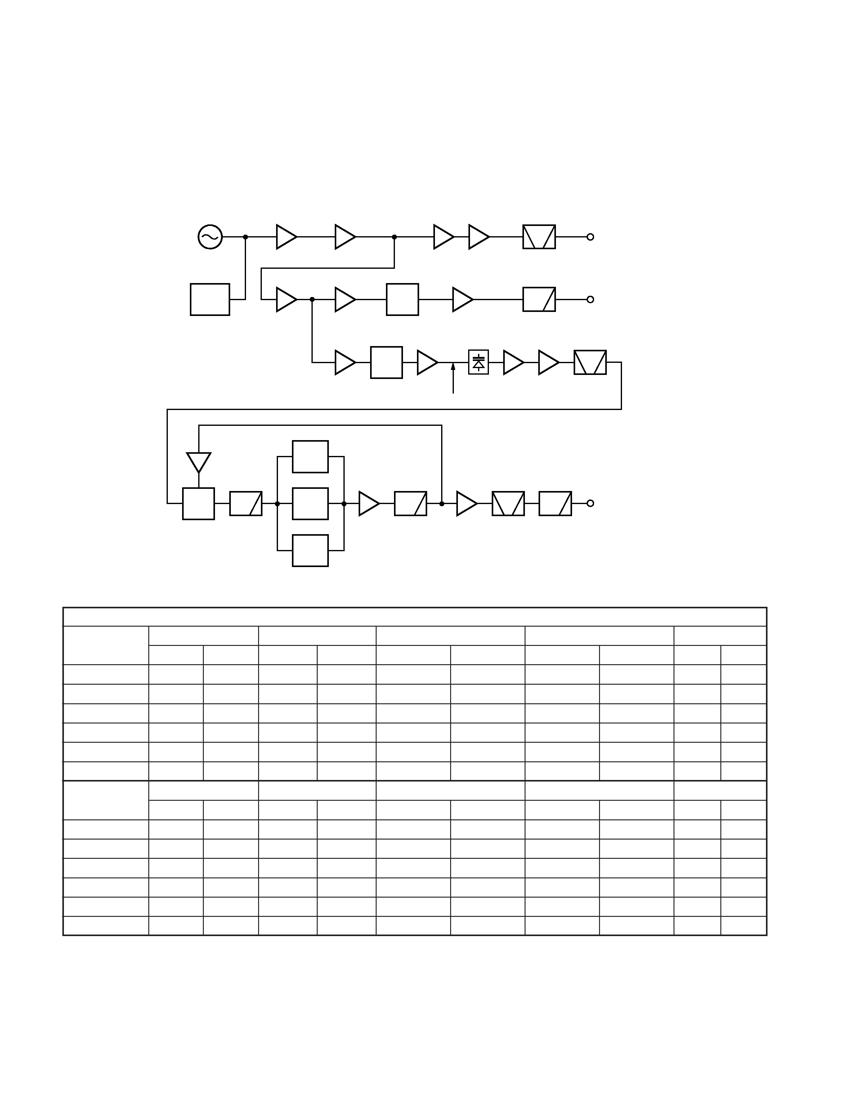
TS-480HX/480SAT
4
CAR (carrier)
The 10.695MHz used in the local oscillation and detection
is generated by the DDS (IC2). The output signal sent from
this DDS passes through a buffer amplifier (Q10) and a low-
pass filter, and is then sent to each signal.
X1,Q1
15.6MHz
TCXO
SO-3
Q4
Buffer
Q3
Q6
Buffer
Q10
Buffer
Q5
x2
Q8
Q12
x2
IC2
DDS
Q2
Q7
Buffer
Q9
Q11
Buffer
IC1
DDS
IC3
PLL
Q451
VCO1
Q452
VCO2
Q456
VCO3
31.2MHz
D1
CF1
BPF
BPF
LPF
FM MOD
Q14
LPF
LPF
BPF
LPF
Q455
Q15
LO1
73.125~
133.095MHz
LO2
62.4MHz
CAR
10.695MHz
8.33~8.47MHz
Fig. 2
Reference signal generator, LO1/LO2/CAR
DDS AD9835BRU (IC1)
HF TX/RX
USB
LSB
CW
CW-R
CWN
Lo1
RX
TX
RX
TX
RX
TX
RX
TX
RX
TX
Filter offset 1
+1.5k
+1.5k
-1.5k
-1.5k
+(1.5k-PITCH) +(1.5k-PITCH) -(1.5k-PITCH) -(1.5k-PITCH)
0
0
Filter offset 2
+0.71k
+0.71k
-0.71k
-0.71k
----
-
-
RIT
(
RIT)
-
(
RIT)
-
(
RIT)
-
(
RIT)
-
(
RIT)
-
XIT
-
(
XIT)
-
(
XIT)
-
(
XIT)
-
(
XIT)
-
(
XIT)
IF Shift
+(IF S)
-
-(IF S)
-
+(IF S)
-
-(IF S)
-
+(IF S)
-
CAR correction +(CAR H) +(CAR H)
-(CAR L)
-(CAR L)
+(CAR H)
+(CAR H)
-(CAR L)
-(CAR L)
-
-
HF TX/RX
CWN-R
FSK
FSK-R
AM
FM
Lo1
RX
TX
RX
TX
RX
TX
RX
TX
RX
TX
Filter offset 1
0
0
-(SHIFT/2) -(SHIFT/2)
-(SHIFT/2)
-(SHIFT/2)
0
0
0
0
Filter offset 2
-
-
-
-
----
-
-
RIT
(
RIT)
-
(
RIT)
-
(
RIT)
-
(
RIT)
-
(
RIT)
-
XIT
-
(
XIT)
-
(
XIT)
-
(
XIT)
-
(
XIT)
-
(
XIT)
IF Shift
-(IF S)
-
-(IF S)
-
+(IF S)
-
-
-
-
-
CAR correction
--
--
----
-
-
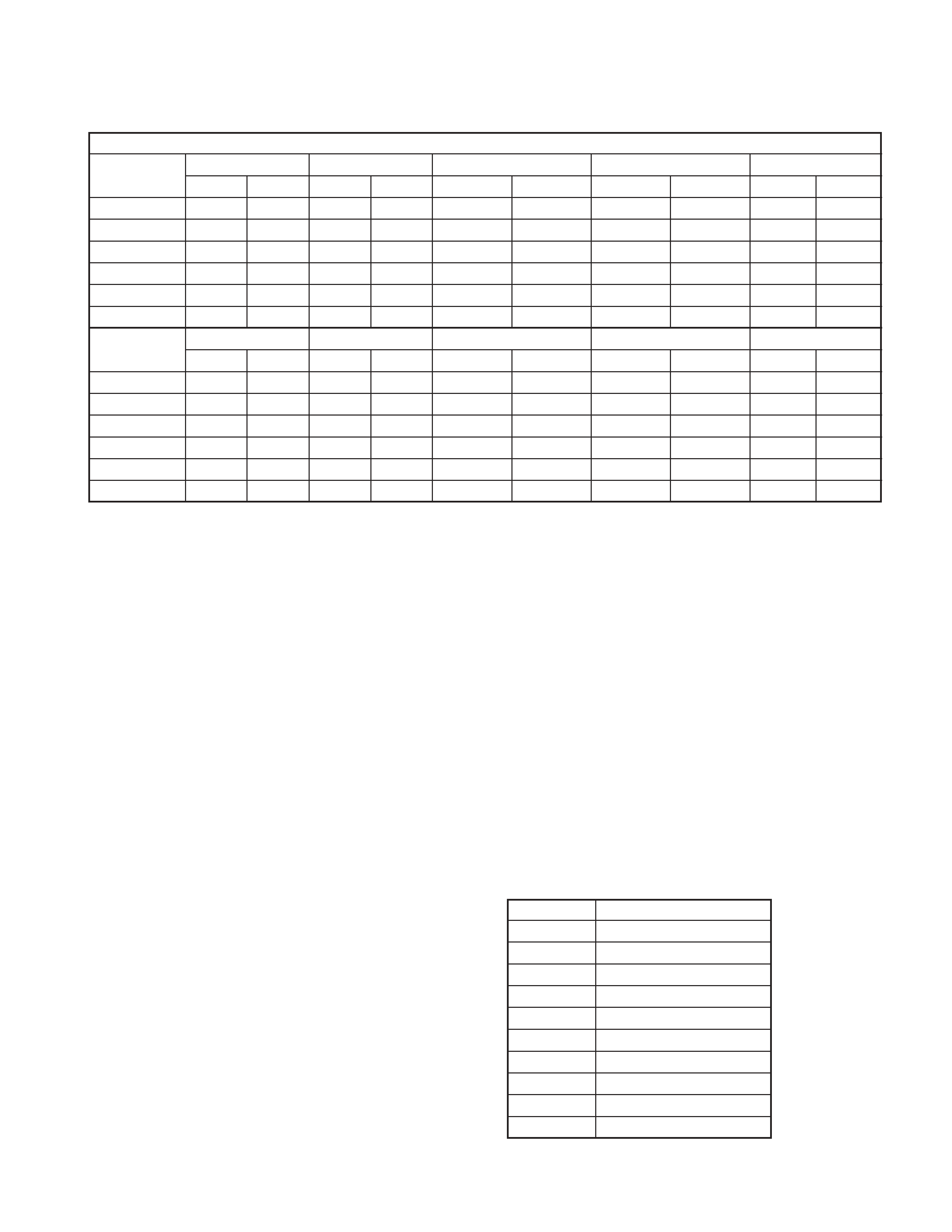
Filter offset 2 : DATA filter ON, The amount of IF shift when selecting Center "2210Hz"
(
RIT) : RIT frequency variable amount (-9.99~+9.99kHz)
(
XIT) : XIT frequency variable amount (-9.99~+9.99kHz)
(PITCH) : CW pitch frequency (400~1000Hz, Initial value 800Hz)
(SHIFT) : FSK shift width frequency (170Hz, 200Hz, 425Hz, 850Hz, Initial value:170Hz)
(MARK) : FSK mark frequency (H TONE : 2125Hz, L TONE : 1275Hz, Initial value : 2125Hz)
Table 1
LO1 frequency shift data
CIRCUIT DESCRIPTION
TS-480HX/480SAT
5
DDS AD9835BRU (IC2)
CAR
USB
LSB
CW
CW-R
CWN
RX
TX
RX
TX
RX
TX
RX
TX
RX
TX
Filter offset 1
+1.5k
+1.5k
-1.5k
-1.5k
+(1.5k-PITCH) +(1.5k-PITCH) -(1.5k-PITCH)
-(1.5k-PITCH)
00
Filter offset 2
+0.71k
+0.71k
-0.71k
-0.71k
-
-
-
-
-
-
CW piitch
-
-
-
-
+(PIITCH)
-
-(PIITCH)
-
+(PIITCH)
-
FSK tone
-
-
-
-
-
-
-
-
-
-
IF Shift
+(IF S)
-
-(IF S)
-
+(IF S)
-
-(IF S)
-
+(IF S)
-
CAR correction +(CAR H) +(CAR H)
-(CAR L)
-(CAR L)
+(CAR H)
+(CAR H)
-(CAR L)
-(CAR L)
-
-
CAR
CWN-R
FSK
FSK-R
AM
FM
RX
TX
RX
TX
RX
TX
RX
TX
RX
TX
Filter offset 1
0
0
-(SHIFT/2) -(SHIFT/2)
-(SHIFT/2)
-(SHIFT/2)
Stop
0
-455k
0
Filter offset 2
-
-
-
-
-
-
-
-
-
-
CW pitch
-(PIITCH)
-
-
-
-
-
-
-
-
-
FSK tone
-
-
-(MARK)
-(MARK) +(MARK+SHIFT)
-(MARK)
-
-
-
-
IF Shift
-(IF S)
-
-(IF S)
-
+(IF S)
-
-
-
-
-
CAR correction
---
-
-
-
-
-
-
-
Filter offset 2 : DATA filter ON, The amount of IF shift when selecting Center "2210Hz"
(
RIT) : RIT frequency variable amount (-9.99~+9.99kHz)
(
XIT) : XIT frequency variable amount (-9.99~+9.99kHz)
(PITCH) : CW pitch frequency (400~1000Hz, Initial value 800Hz)
(SHIFT) : FSK shift width frequency (170Hz, 200Hz, 425Hz, 850Hz, Initial value:170Hz)
(MARK) : FSK mark frequency (H TONE : 2125Hz, L TONE : 1275Hz, Initial value : 2125Hz)
Table 2
CAR frequency shift data
Receiver Circuit
FM mode operates in a triple conversion: the first IF
(73.095MHz), the second IF (10.695MHz), and the third IF
(455kHz). All modes other than FM mode operate in a double
conversion: the first IF (73.095MHz), and the second IF
(10.695MHz).
From antenna to a preamplifier (Q153, 154)
There are two antenna terminals: ANT 1 and ANT 2. With
these antenna terminals, it is possible to select the terminal
to be used and store the selection for each band. A pigtail
wire is used in this transceiver to maintain the freedom of the
antenna wire when it is mounted in a car.
The receive signal sent from the antenna terminal enters
the ANT section (X45-366 C/3 : 200W transceiver, X45-365 C/
3 : 100W transceiver) of the final unit. The signal passes
through a surge trap, the antenna changeover relay, the an-
tenna tuner changeover relay (only 100W transceiver), the
transmission/reception changeover relay, and an image filter,
and is then sent from CN503 to CN2 of the RF unit (X44-327)
though a co-axial cable.
The signal input into the RF unit passes through the at-
tenuator circuit, the image filter, the surge absorption limiter,
and then enters the RF BPF. Although the default of the at-
tenuator is 12dB, it can change to approximately 20dB by re-
moving the CN4 jumper.
The RF BPF divides in the range as shown in table 3. The
transmit signal also passes through the RF BPF when trans-
mitting.
The preamplifier (Q153, 154) receives the signal passed
through the RF BPF. This transceiver obtains necessary gain
and frequency characteristic by applying NFB (Negative
Feedback) to the source earthed circuit having two parallel-
connected MOS FETs. Although the preamplifier was con-
ventionally switched by switching between low-band and
high-band, this transceiver can obtain necessary characteris-
tics for each band by switching the NFB amount of the
source at Q155.
You can turn the preamplifier ON/OFF by pressing the
[ATT/PRE] key.
Band
Filter range
BC
30kHz~1.705MHz
1.8MHz
1.705~2.5MHz
3.5MHz
2.5~4.1MHz
7MHz
4.1~7.5MHz
10MHz
7.5~10.5MHz
14MHz
10.5~14.5MHz
21MHz
14.5~21.5MHz
28MHz
21.5~30MHz
30~49MHz, 54~60MHz
50MHz
49~54MHz
Table 3
RF BPF
CIRCUIT DESCRIPTION