© 2003-10 PRINTED IN JAPAN
B51-8663-00 (N) 743
VHF FM TRANSCEIVER
TM-271A/271E
SERVICE MANUAL
CIRCUIT DESCRIPTION ............................ 2
SEMICONDUCTOR DATA ........................ 8
COMPONENTS DESCRIPTION ................ 9
PARTS LIST ............................................. 10
EXPLODED VIEW .................................... 17
PACKING ................................................. 18
RESETTING THE TRANSCEIVER ........... 19
ADJUSTMENT ........................................ 20
TERMINAL FUNCTION ........................... 27
PC BOARD
DISPLAY UNIT (X54-3450-10) ............ 28
TX-RX UNIT (X57-685X-XX) ............... 30
SCHEMATIC DIAGRAM .......................... 34
BLOCK DIAGRAM ................................... 38
LEVEL DIAGRAM .................................... 40
SPECIFICATION ................... BACK COVER
CONTENTS
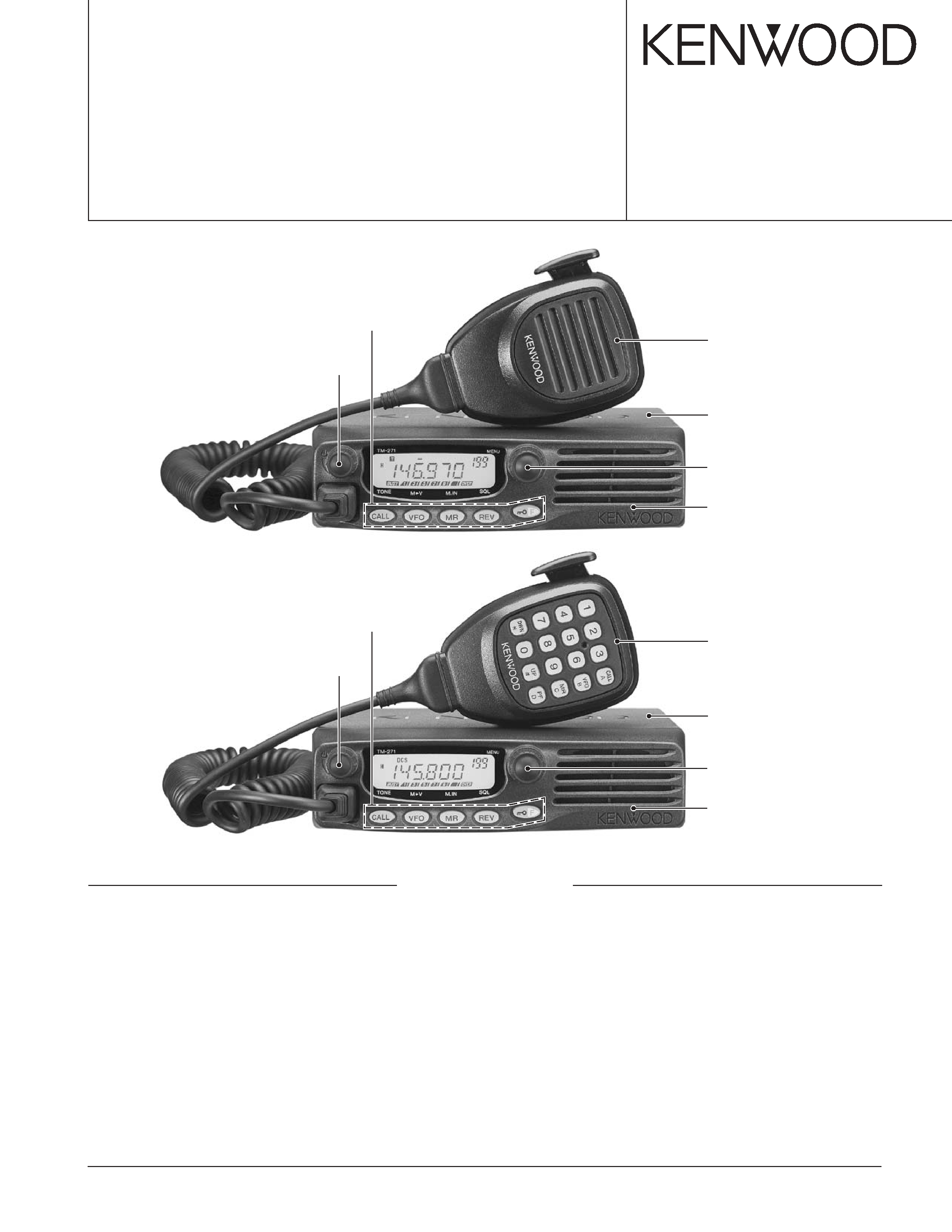
Microphone
(T91-0624-05)
Cabinet
(A01-2193-01)
Panel assy
(A62-1088-03)
Knob (Encoder)
(K29-9293-03)
Knob (Volume)
(K29-9292-03)
Key top
(K29-9291-01)
Microphone
(T91-0641-05)
Cabinet
(A01-2193-01)
Panel assy
(A62-1088-03)
Knob (Encoder)
(K29-9293-03)
Knob (Volume)
(K29-9292-03)
Key top
(K29-9291-01)
TM-271A (M2,M4)
TM-271A/E (K,M3,E)
TM-271A/271E
2
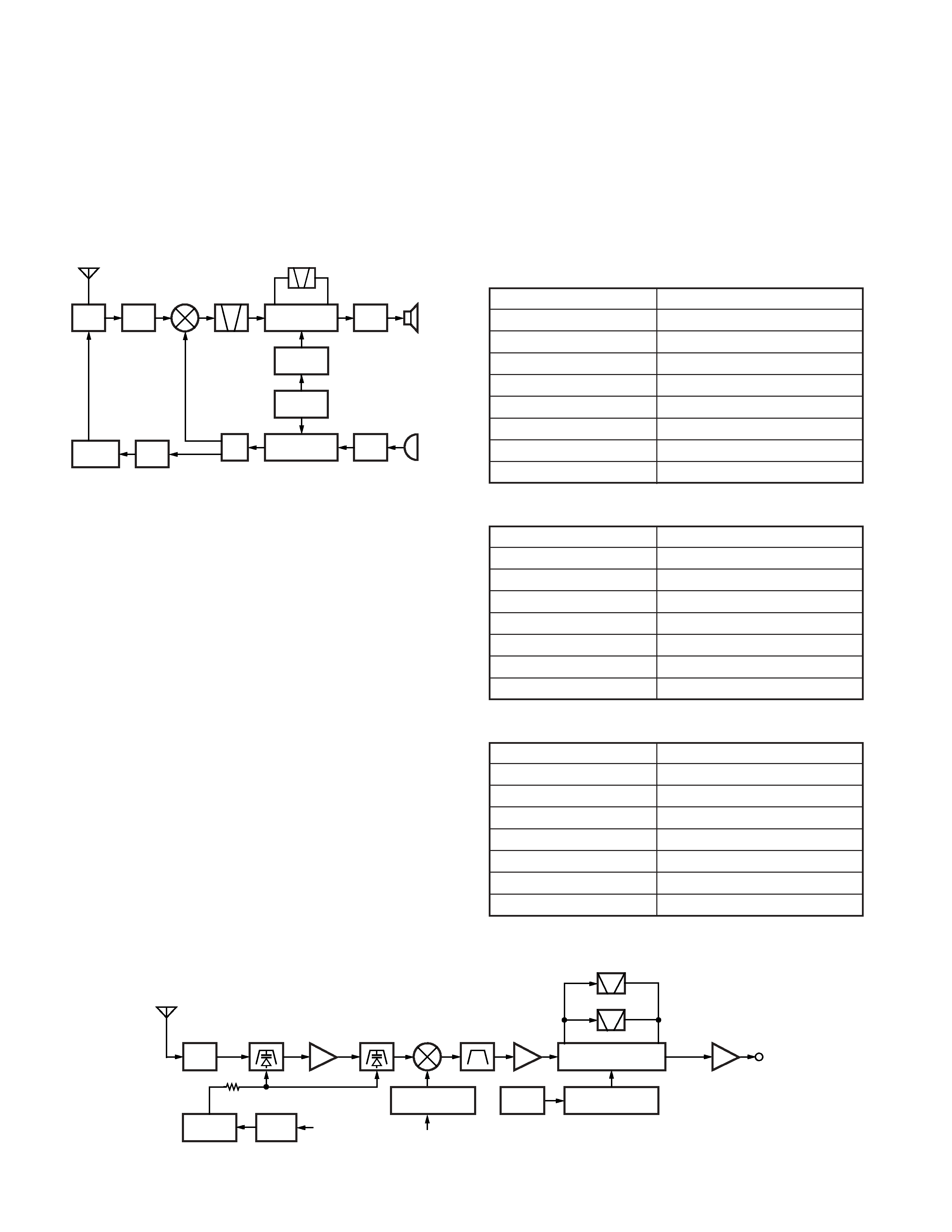
Frequency Configuration
The receiver utilizes double conversion. The first IF is
49.95MHz and the second IF is 450kHz. The first local oscil-
lator signal is supplied from the PLL circuit.
The PLL circuit in the transmitter generates the necessary
frequencies. Figure 1 shows the frequencies.
CIRCUIT DESCRIPTION
Receiver System
The receiver is double conversion superheterodyne. The
frequency configuration is shown in Figure 1.
Front-end RF Amplifier
An incoming signal from the antenna is applied to an RF
amplifier (Q353) after passing through a transmit/receive
switch circuit (D603, D605 are off) and a band pass filter
(L357, L356 and varactor diodes : D353, D354). After the
signal is amplified (Q353), the signal is filtered through a band
pass filter (L354, L355 and varactor diodes: D351, D352) to
eliminate unwanted signals before it is passed to the first
mixer.
The voltage of these diodes are controlled by tracking the
CPU (IC101) center frequency of the band pass filter. (See
Fig. 2.)
First Mixer
The signal from the RF amplifier is heterodyned with the
first local oscillator signal from the PLL frequency synthesizer
circuit at the first mixer (Q352) to create a 49.95MHz first
intermediate frequency (1st IF) signal. The first IF signal is
then fed through one pair of monolithic crystal filter (MCF :
XF351) to further remove spurious signals.
ANT
SW
RF
AMP
1st
MIX
AF
PA
TCXO
MIC
AMP
X3
multiply
RF
AMP
POWER
AMP
CF 450kHz
MCF
49.95MHz
IF SYSTEM
PLL/VCO
16.8MHz
50.4MHz
ANT
RX
TX
SP
MIC
1/2
Fig. 1
Frequency configuration
IF Amplifier
The first IF signal is amplified by Q351, and then goes to
IC301 (FM processing IC). The signal is heterodyned again
with a second local oscillator signal within IC301 to create a
450kHz second IF signal. The second IF signal is then fed
through a 450kHz ceramic filter (Wide : CF301, Narrow :
CF302) to further eliminate unwanted signals before it is am-
plified and FM detected in IC301.
Item
Rating
Nominal center frequency
49.95MHz
Pass bandwidth
±5.0kHz or more at 3dB
35dB stop bandwidth
±20.0kHz or less
Ripple
1.0dB or less
Insertion loss
5.0dB or less
Guaranteed attenuation
80dB or more at fo
±1MHz
Spurious
40dB or more
Terminal impedance
350
/ 5.5pF
Table 1
Crystal filter (L71-0620-05) : XF351
Item
Rating
Nominal center frequency
450kHz
6dB bandwidth
±6.0kHz or more
50dB bandwidth
±12.5kHz or less
Ripple
2.0dB or less
Insertion loss
6.0dB or less
Guaranteed attenuation
35.0dB or more within fo
±100kHz
Terminal impedance
2.0k
Table 2
Ceramic filter (L72-0993-05) : CF301
Item
Rating
Nominal center frequency
450kHz
6dB bandwidth
±4.5kHz or more
50dB bandwidth
±10.0kHz or less
Ripple
2.0dB or less
Insertion loss
6.0dB or less
Guaranteed attenuation
60.0dB or more within fo
±100kHz
Terminal impedance
2.0k
Table 3
Ceramic filter (L72-0999-05) : CF302
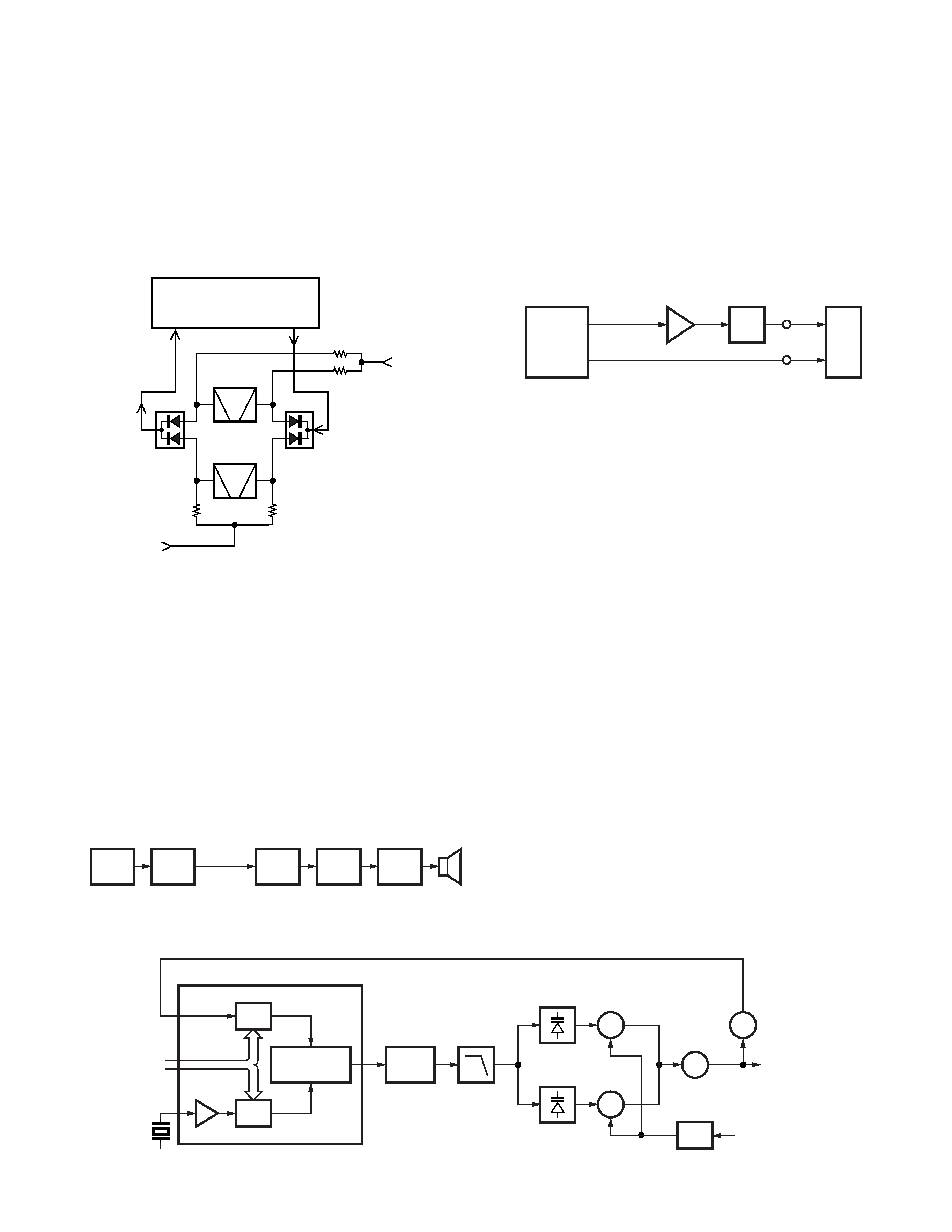
ANT
L357,356
D353,354
BPF
Q353
RF AMP
Q351
IF AMP
IC161
D/A CONVERTER
Q352
MIX
XF351
MCF
D602
D603
D605
ANT
SW
IC161
D/A
IC203
DC AMP
Q302
X3 multiply
IC402
1/2 divider
X401
TCXO
IC301
IF system
1st local
OSC (VCO/PLL)
W/NO
(EVOL2)
CF301 (Wide)
CF302 (Narrow)
TV
CPU
L354,355
D351,352
BPF
Fig. 2
Receiver system
TM-271A/271E
3
Wide/Narrow Switching Circuit
The Wide port (pin 65) and Narrow port (pin 64) of the CPU
is used to switch between ceramic filters. When the Wide
port is high, the ceramic filter SW diodes (D303, D302) cause
CF301 to turn on to receive a Wide signal.
When the Narrow port is high, the ceramic filter SW di-
odes (D303, D302) cause CF302 to turn on to receive a Nar-
row signal. (See Fig. 3.)
AF Signal System
The detection signal from IF IC (IC301) goes to D/A con-
verter (IC161) to adjust the gain and is output to AF filter
(IC251) for characterizing the signal. The AF signal output
from IC251 and the DTMF signal, BEEP signal are summed
and the resulting signal goes to the D/A converter (IC161).
The AFO output level is adjusted by the D/A converter. The
signal output from the D/A converter is input to the audio
power amplifier (IC252). The AF signal from IC252 switches
between the internal speaker and speaker jack (J1) output.
(See Fig. 4.)
Squelch Circuit
The detection output from the FM IF IC (IC301) passes
through a noise amplifier (Q301) to detect noise. A voltage is
applied to the CPU (IC101). The CPU controls squelch ac-
cording to the voltage (SQIN) level. The signal from the RSSI
pin of IC301 is used for S-meter. The electric field strength of
the receive signal can be known before the SQIN voltage is
input to the CPU, and the scan stop speed is improved.
Narrow
IC101 64pin
IF_IN
MIX_O
IC301
IF System
CF302
(Narrow)
CF301
(Wide)
R320
R319
R317
R318
D303
D302
Wide
IC101 65pin
AF
Filter
D/A
CONV.
D/A
CONV.
IC161
IC251
IC161
W/NO
(EVOL2)
AF PA
IC252
SP
IF IC
IC301
Q301
NOISE AMP
D301
IC301
IC101
AFO
RSSI
DET
CPU
IF
SYSTEM
SQIN
RSSI
Fig. 3
Wide/Narrow switching circuit
Fig. 4
AF signal system
Fig. 5
Squelch circuit
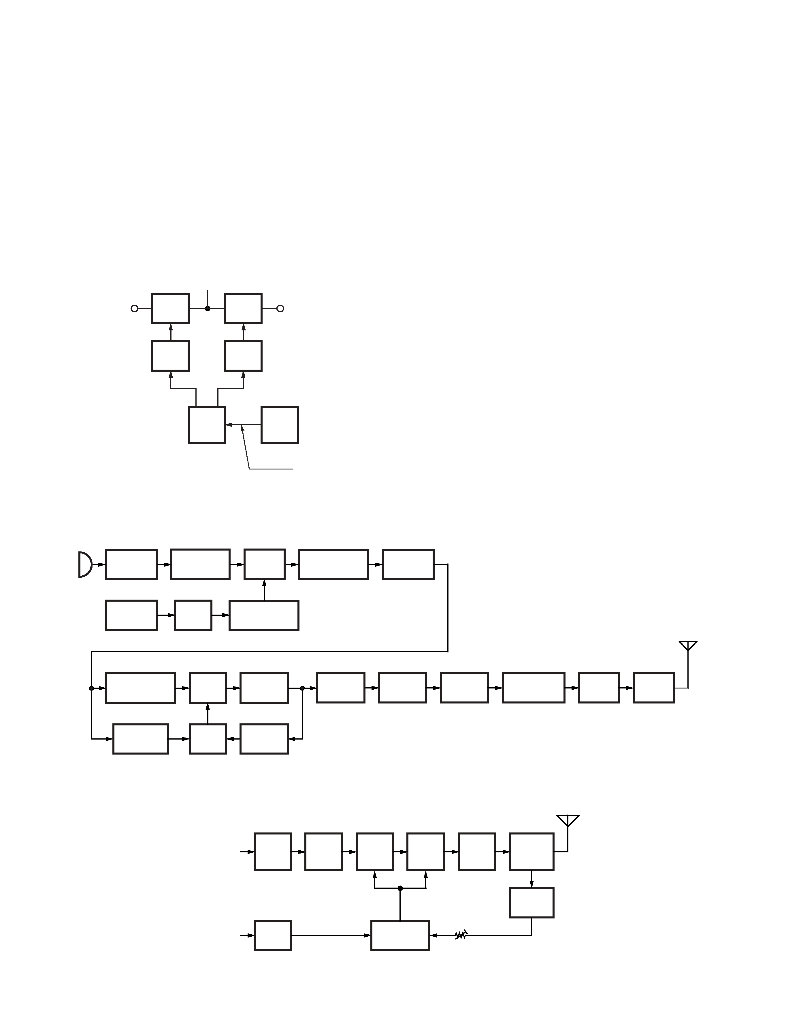
PLL Frequency Synthesizer
The PLL circuit generates the first local oscillator signal for
reception and the RF signal for transmission.
PLL
The frequency step of the PLL circuit is 5 or 6.25kHz. A
16.8MHz reference oscillator signal is divided at IC401 by a
fixed counter to produce the 5 or 6.25kHz reference fre-
quency. The voltage controlled oscillator (VCO) output signal
is buffer amplified by Q410, then divided in IC401 by a dual-
module programmable counter. The divided signal is com-
pared in phase with the 5 or 6.25kHz reference signal in the
phase comparator in IC401. The output signal from the
phase comparator is filtered through a low-pass filter and
passed to the VCO to control the oscillator frequency. (See
Fig. 6.)
VCO
The operating frequency is generated by Q406 in transmit
mode and Q405 in receive mode. The oscillator frequency is
controlled by applying the VCO control voltage, obtained
from the phase comparator, to the varactor diodes (D405 and
D406 in transmit mode and D403 and D404 in receive mode).
The TX/RX pin is set high in receive mode causing Q408 and
Q407 to turn Q406 off, and turn Q405 on. The TX/RX pin is
set low in transmit mode. The outputs from Q405 and Q406
are amplified by Q410 and sent to the RF amplifiers. (See Fig.
6.)
D405,406
Q406
TX VCO
Q410
BUFF
AMP
D403,404
Q405
RX VCO
Q407,408
T/R SW
Charge
pump
LPF
Phase
comparator
1/M
1/N
5kHz/6.25kHz
5kHz/6.25kHz
REF
OSC
16.8MHz
PLL
DATA
IC401 : PLL IC
Q404
AMP
RF amplifiers
Q402,403
TX/RX (CPU)
Fig. 6
PLL circuit
CIRCUIT DESCRIPTION
TM-271A/271E
4
Unlock Circuit
During reception, the 8RC signal goes high, the 8TC signal
goes low, and Q34 turns on. Q33 turns on and a voltage is
applied to 8R. During transmission, the 8RC signal goes low,
the 8TC signal goes high and Q36 turns on. Q35 turns on and
a voltage is applied to 8T.
The CPU monitors the PLL (IC401) LD signal directly.
When the PLL is unlocked during transmission, the PLL LD
signal goes low. The CPU detects this signal and makes the
8TC signal low. When the 8TC signal goes low, no voltage is
applied to 8T, and no signal is transmitted. (See Fig. 7.)
IC101
CPU
Q34
SW
Q33
SW
IC401
PLL
Q36
SW
Q35
SW
LD
8RC
8C
8R
8T
8TC
PLL lock
: LD "H"
Fig. 7
Unlock circuit
Transmitter System
Outline
The transmitter circuit produces and amplifies the desired
frequency directly. It FM-modulates the carrier signal by
means of a varicap diode.
Power Amplifier Circuit
The transmit output signal from the VCO passes through
the transmission/reception selection diode (D409) and ampli-
fied by Q501, Q502 and Q503. The amplified signal goes to
the final amplifier (Q504) through a low-pass filter. The low-
pass filter removes unwanted high-frequency harmonic com-
ponents, and the resulting signal is transmitted through the
antenna terminal. (See Fig. 8.)
APC Circuit
The automatic transmission power control (APC) circuit
detects part of a final amplifier output with a diode (D606,
D607) and applies a voltage to IC501. IC501 compares the
APC control voltage (PC) generated by the D/A converter
(IC161) and DC amplifier (IC203) with the detection output
voltage. IC501 generates the voltage to control Q503 and
Q504 and stabilizes transmission output.
The APC circuit is configured to protect over current of
Q503 and Q504 due to fluctuations of the load at the antenna
end and to stabilize transmission output at voltage and tem-
perature variations. (See Fig. 9.)
RF
AMP
Q501
DRIVE
AMP
Q503
FINAL
AMP
Q504
PRE
DRIVE
AMP
Q502
DC
AMP
IC203
ANT
SW
D602,D603
D605
LPF
ANT
POWER
DET
D606
D607
IC501
VR601
APC
CONTROL
D409
IC161
(PC/TVO)
(PC)
Q411
RF AMP
Q501
RF AMP
Q502
PRE
DRIVE AMP
Q503
ANT
DRIVE
AMP
Q504
FINAL
AMP
IC402
1/2
DIVIDER
IC161
Q406
D/A
CONVERTER
D/A
CONVERTER
D/A
CONVERTER
X401
TCXO
16.8MHz
VCO
IC401
PLL
Q410
BUFFER
Q404
RF AMP
IC203
BUFFER
IC101
IC161
MIC KEY
INPUT
CPU
IC161
IC203
SUM
AMP
IC202
IC201
MIC
MIC/IDC
SPLATTER
FILTER
Fig. 9
APC circuit
Fig. 8
Transmitter system
CIRCUIT DESCRIPTION
TM-271A/271E
5
Control Circuit
The CPU carries out the following tasks (See Fig. 10.):
1) Controls the WIDE, NARROW, TX/RX outputs.
2) Adjusts the AF signal level of the AF filter (IC251) and
turns the filter select compounder on or off.
3) Controls the display unit.
4) Controls the PLL (IC401).
5) Controls the D/A converter (IC161) and adjusts the vol-
ume, modulation and transmission power.
Memory Circuit
The transceiver has an 64k-bit EEPROM (IC66). The
EEPROM contains adjustment data. The CPU (IC101) con-
trols the EEPROM through three serial data lines. (See Fig.
11.)
IC161
D/A
converter
IC401
PLL
IC101
CPU
LD
DT
CK
PLLE
EEPCK
IC101
CPU
IC66
EEPROM
EEPSDT
EEPWP
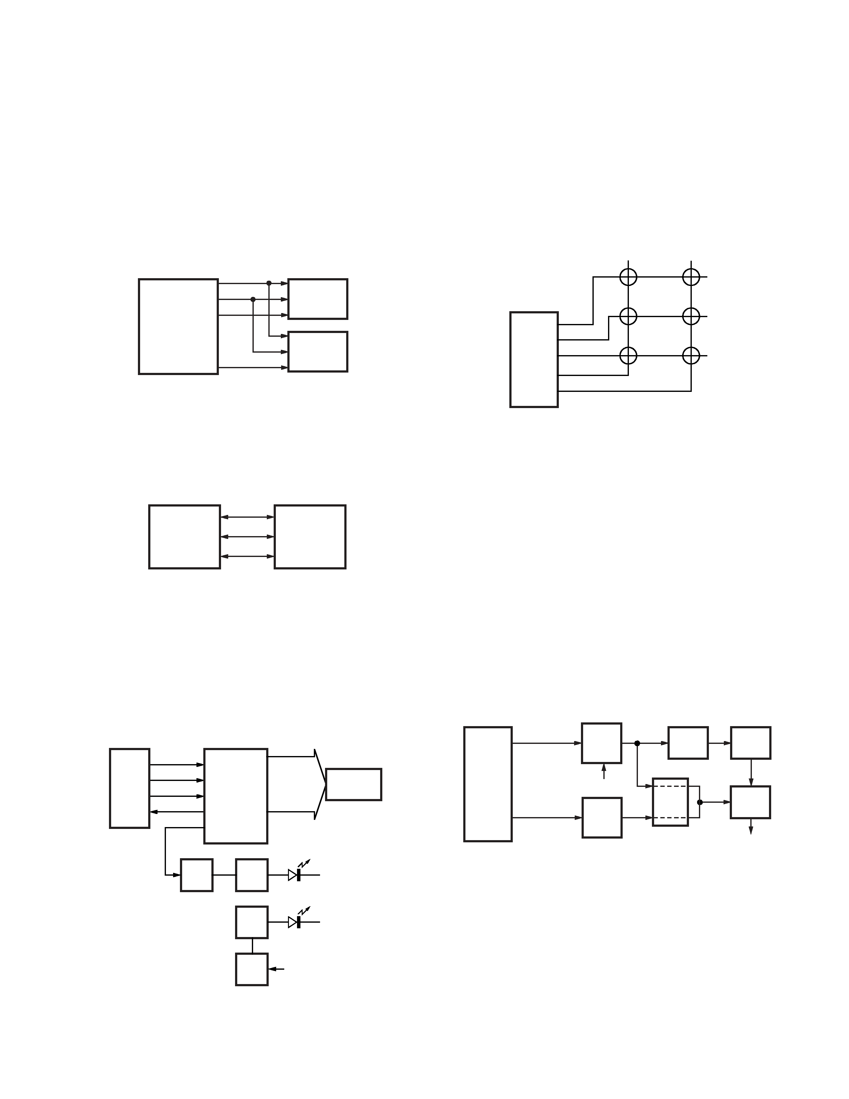
Display Circuit
The CPU (IC101) controls the display LCD and LEDs.
When power is on, the LCD driver will use the BL line to con-
trol the LCD illumination and key backlight LEDs.
The brightness function is controlled by the switch Q12.
The LCD driver (IC3) and CPU (IC101) communicate through
the CE, CL, DI, DO lines. (See Fig. 12.)
Key Matrix Circuit
The TM-271 front panel has function keys. Each of them
is connected to a cross point of a matrix of the KI1 to KI3 and
KSI to KS2 ports of the LCD driver.
The LCD driver monitors the status of the KI1 to KI3 and
KS1 to KS2 ports. If the state of one of the ports changes,
the LCD driver assumes that the key at the matrix point corre-
sponding to that port has been pressed.
Encode
The DCS and CTCSS signals are output from QT/DQT of
the CPU (IC101) and summed with the external pin DI line by
the summing amplifier (IC203) and the resulting signal goes
to the D/A converter (IC161). The DTMF signal is output from
DTMF pin of the CPU and summed with a MIC signal by the
summing amplifier (IC203), and the resulting signal goes to
the D/A converter (IC161).
The D/A converter (IC161) adjusts the MOD level and the
balance between the MOD and CTCSS/DCS levels. Part of a
CTCSS/DCS signal is summed with MOD and the resulting
signal goes to the VCOMOD pin of the VCO. This signal is
applied to a varicap diode in the VCO for direct FM modula-
tion.
IC3
LCD
driver
KI1
KI2
KI3
KS2
KS1
FUNC
REV
CALL
VFO
MR
MHz
(Encoder)
X401
TCXO
IC161
D/A
VCO
IC203
SUM
AMP
IC203
SUM
AMP
IC401
PLL
TCXO
MOD
VCO
MOD
Amp
DI
QT/DQT
(CPU1)
DTMO
(EVOL15)
IC101
CPU
TONE
DTMF
Fig. 10
Control circuit
Fig. 11
Memory circuit
Q10
SW
Q6
SW
IC101
CPU
D2~D4
Q9
SW
D19~D30
Q12
SW
IC3
LCD
driver
CE
CL
DI
DO
BL
COM0~
COM3
SEG0~
SEG30
LCD
BRI
Fig. 12
Display circuit
Fig. 13
Key matrix circuit
Fig. 14
Encoder
CIRCUIT DESCRIPTION