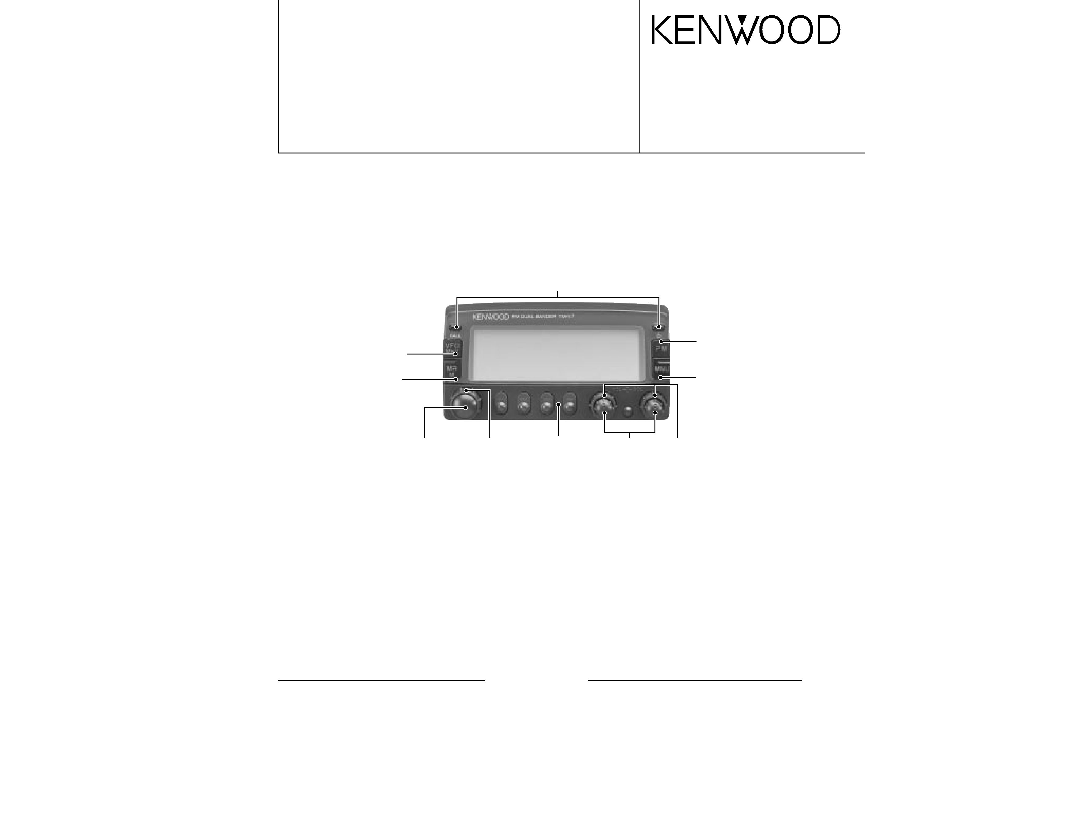
CONTROL PANEL
RC-V7
© 2002-2 PRINTED IN JAPAN
B51-8624-00 (S) 434
SERVICE MANUAL
CIRCUIT DESCRIPTION ....................................... 2
SEMICONDUCTOR DATA ................................... 3
TERMINAL FUNCTION ........................................ 3
PARTS LIST .......................................................... 4
EXPLODED VIEW ................................................. 5
PACKING .............................................................. 6
PC BOARD VIEWS
TX-RX UNIT (X57-6620-20) (C/3) .................. 7
SCHEMATIC DIAGRAM ....................................... 9
BLOCK DIAGRAM .............................................. 11
SPECIFICATIONS ............................ BACK COVER
Button knob (PWR, CALL)
(K27-3165-03)
Button knob (MR)
(K27-3167-33)
Knob (VOL)
(K29-5222-03)
Button knob
(MAIN, PUSH)
(K27-3175-03)
Knob (SQL)
(K29-5223-03)
Panel assy
(A62-1048-03)
Knob (MAIN)
(K29-5221-03)
Button knob (PM)
(K27-3168-23)
Button knob (MNU)
(K27-3169-33)
Button knob (VFO)
(K27-3166-23)
CONTENTS
RC-V7
2
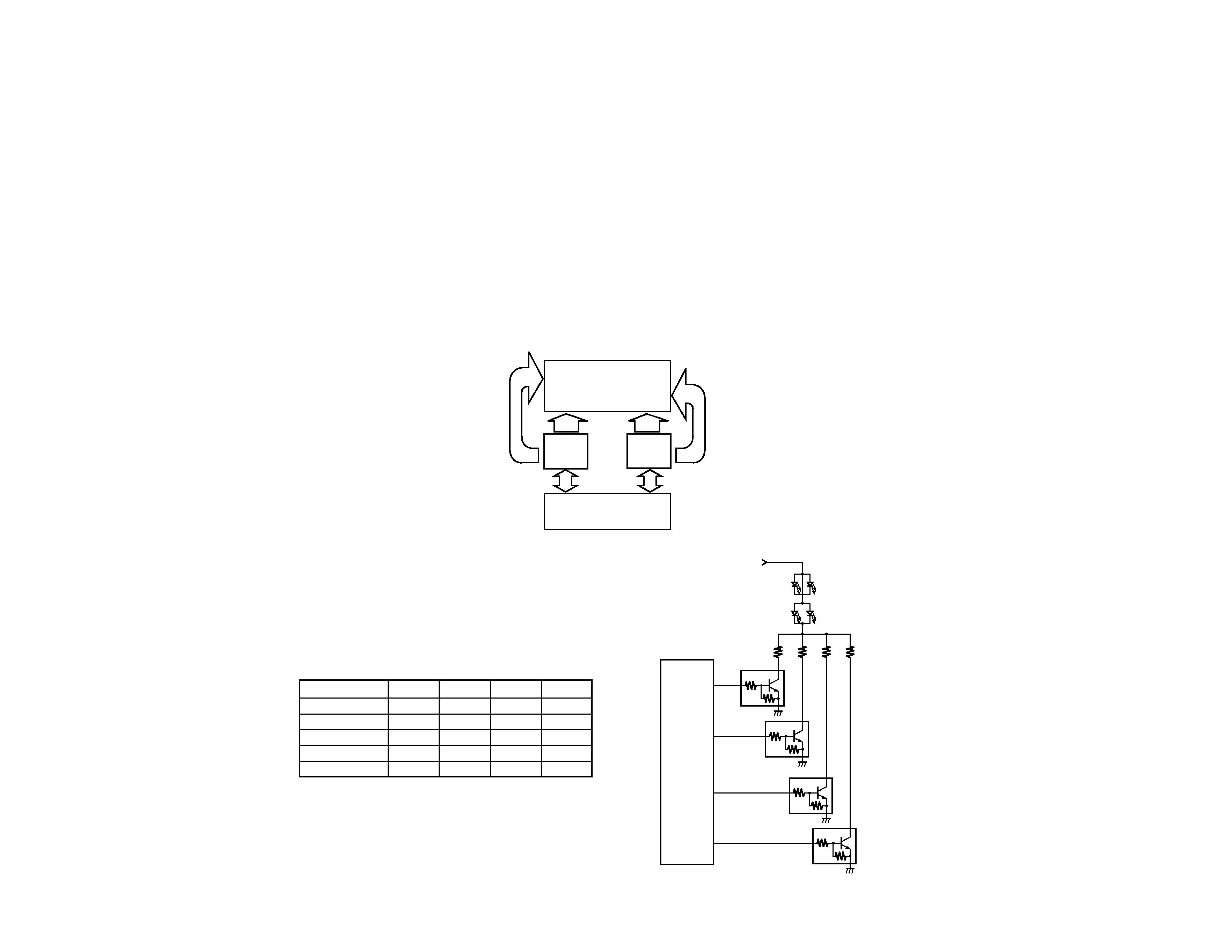
CIRCUIT DESCRIPTION
Panel Section (LCD ASSY: B38-0772-65)
The panel section controls serial communications with the
main unit control section, the key input circuit, the display
circuit, and the dimmer circuit through the microprocessor
(IC4).
· Serial communications circuit
A buffer is inserted in order to protect the microprocessor
ports.
· Key input circuit
There is one microprocessor port for each panel section
key. The PSW key is pulled down and the other keys are pulled
up with software within the microprocessor. The rotary encoder
is input directly to the microprocessor.
· Display circuit
Display section is a 152x45-dot full-dot matrix LCD controlled
by two LCD. As shown in Figure 1, the master IC (IC5) side is
connected to 32 common dots and 80 segment dots and the
slave IC (IC6) side is connected to 13 common dots and 72
segment dots. The LCD drive voltage is obtained by raising
the power supply voltage (5V) within the IC. Also, the contrast
level (LEBEL8) for resetting is adjusted with R19 to be optimum.
LCD
152 X 45(dot)
LCD
Driver
IC 5
LCD
Driver
IC 6
Microprocessor
IC4
80
SEG
72
SEG
32
COM
13
COM
Fig. 1 Display circuit
· Dimmer circuit
The dimmer circuit switches the lamp brightness to one of
four levels or OFF. (See Table 1.) The current flowing to the
LEDs is varied by selecting resistors from R55 to R58.
P60
P61
P62
P63
IC4
Microprocessor
R58
R57
R56
R55
9V
Q11
Q10
LED3
LED1
LED4
LED2
Q13
Q12
Fig. 2 Dimmer circuit
Dimmer level
P60
P61
P62
P63
1H
L
L
L
2L
H
L
L
3L
L
H
L
4L
L
L
H
OFF
LL
LL
Table 1 Port logic
RC-V7
3
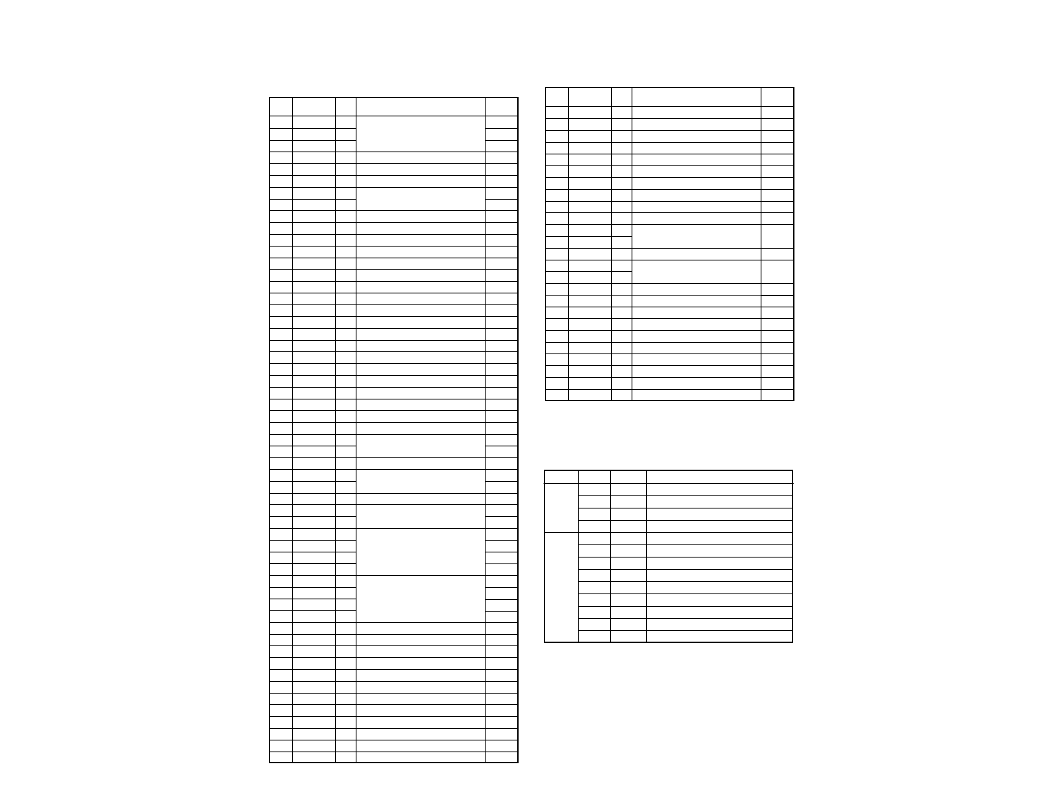
SEMICONDUCTOR DATA / TERMINAL FUNCTION
56
P_KEY5
I
F KEY
L
57
P_KEY6
I
TONE KEY
L
58
P_KEY7
I
REV KEY
L
59
P_KEY8
I
LOW KEY
L
60
RESET
I
Reset input
61
P_ENCCK
I
Encoder clock (encoder A signal)
62
P_INT1
I
Connected to P_SI
63
P_PWR
I
Power switch
64
P_ENCDT
I
Encoder data (encoder B signal)
65
P_BCHK
I
Power voltage check
66
P05/INTP5
I
Connected to VSS
67
P06/INTP6
I
68
VDD
Microprocessor power
69
X2
Clock oscillator connection (4.19M)
70
X1
71
IC (VPP)
72
XT2
73
XT1/P07
74
AVDD
A/D converter analog power
75
AVREF
A/D converter reference voltage
76
P_SQLU
I
430MHz band squelch input
77
P_VOLU
I
430MHz band volume input
78
P_SQLV
I
144MHz band squelch input
79
P_VOLV
I
144MHz band volume input
80
P14/AN14
I
Connected to VSS
Pin
Pin
I/O
Function
Active
No.
code
level
TERMINAL FUNCTION
LCD ASSY (B38-0772-65)
CN1
1
PSO
Serial data output
2
PSI
Serial data input
3
PE
Panel ground
4
PB
Panel power
CN2
1
E
GND
2
SQU
UHF band spuelch input
3
VOLU
UHF band volume input
4
SWU
UHF band select switch input
5
VCC
Reference voltage input
6
SQV
VHF band squelch input
7
VOLV
VHF band volume input
8
SWV
VHF band select switch input
9
E
GND
CN No. Pin No.
Name
Function
78058GCC678BT (LCD ASSY : IC4)
1
P15/AN15
I
2
P16/AN16
I
Connected to VSS
3
P17/AN17
I
4AVSS
A/D converter reference ground
5
P_LCDLE
O
LCD driver latch enable
6
P131/AN01
I
Connected to VSS
7AVREF1
Connected to VDD
8
P70/RXD
I
9
P71/TXD
I
Connected to VSS
10
P72/ASCK
I
11
P_LCDRST
O
LCD driver reset
12
P_LCDDI
O
LCD driver data select (AO)
13
P_LCDWR
O
LCD driver write select
14
P_LCDCE1
O
LCD driver chip select 1
15
P_LCDCE2
O
LCD driver chip select 2
16
P_SI
I
Common microprocessor SO
17
P_SO
O
Common microprocessor SI
18
P27/SCK0 I/O
Not used (Open)
19
P_LCDDT0
O
LCD driver data line 0
20
P_LCDDT1
O
LCD driver data line 1
21
P_LCDDT2
O
LCD driver data line 2
22
P_LCDDT3
O
LCD driver data line 3
23
P_LCDDT4
O
LCD driver data line 4
24
P_LCDDT5
O
LCD driver data line 5
25
P_LCDDT6
O
LCD driver data line 6
26
P_LCDDT7
O
LCD driver data line 7
27
P_LED5
O
LED5 CLF dark lighting
28
P51/A9
I
Connected to VSS
29
P52/A10
I
30
P_5CSW
O
SW 5C control
31
P54/A12
I
Connected to VSS
32
P55/A13
I
33
VSS
Microprocessor ground
34
P56/A14
I
Connected to VSS
35
P57/A15
I
36
P60
I
37
P61
I
Connected to VDD
38
P62
I
39
P63
I
40
P64/RD
O
41
P65/WR
O
Connected to VSS
42
P66/WAIT
I
43
P67/ASTB
I
44
P_DIM
O
CFL dimmer adjustment
45
P31/TO1
I
Connected to VSS
46
P_KEY9
I
PM KEY
L
47
P_KEY10
I
MENU KEY
L
48
P_KEY11
I
CONT KEY
L
49
P-PCL
O
LCD driver clock
50
P_KEY12
I
B. SEL KEY (VHF)
L
51
P_KEY13
I
B. SEL KEY (UHF)
L
52
P_KEY1
I
VFO KEY
L
53
P_KEY2
I
MR KEY
L
54
P_KEY3
I
CALL KEY
L
55
P_KEY4
I
MHz KEY
L
Pin
Pin
I/O
Function
Active
No.
code
level
RC-V7
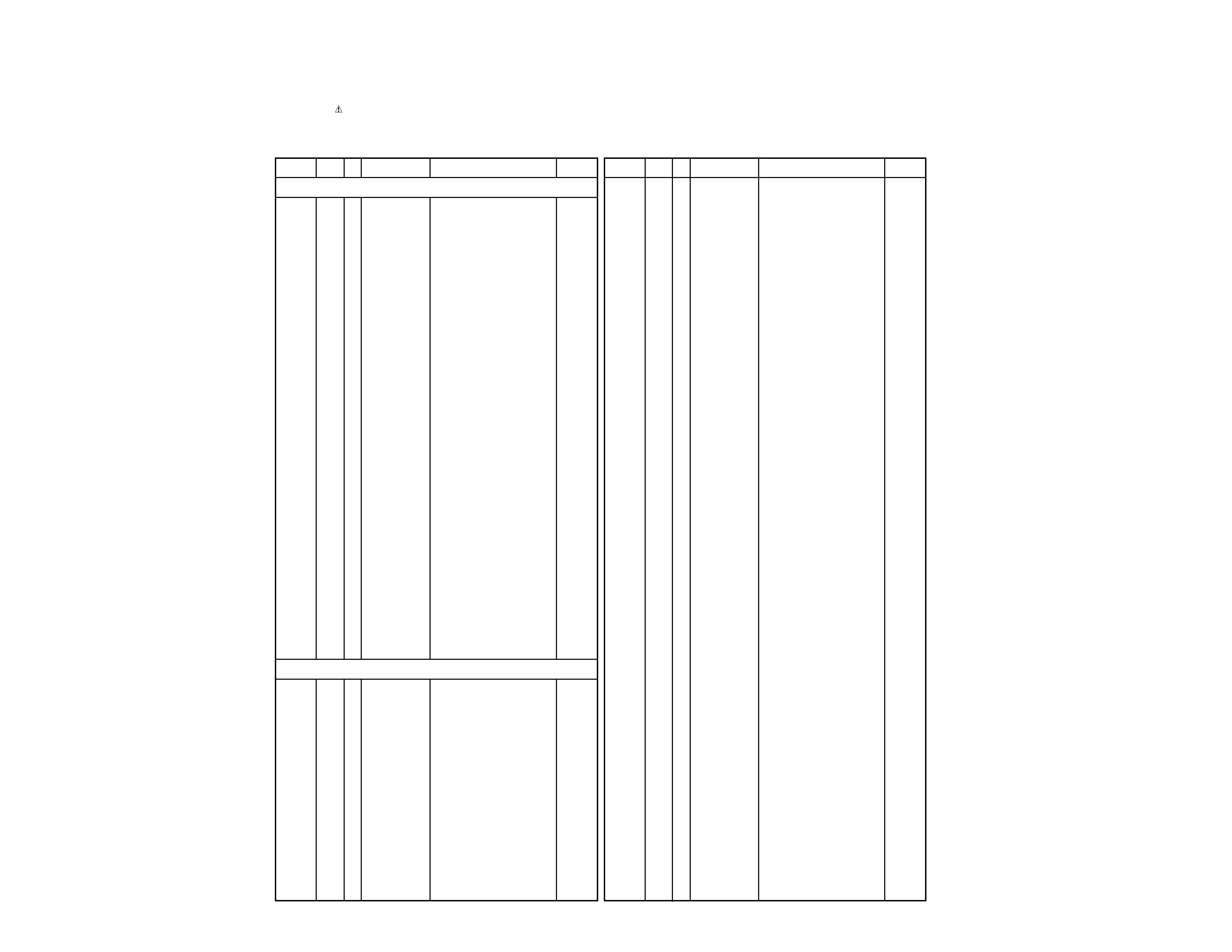
PARTS LIST
4
Parts No.
Description
Address
New
parts
Destination
Destination
RC-V7
Ref. No.
Parts No.
Description
Address
New
parts
New Parts.
indicates safety critical components.
Parts without Parts No. are not supplied.
Les articles non mentionnes dans le Parts No. ne sont pas fournis.
Teile ohne Parts No. werden nicht geliefert.
RC-V7 (Y62-4980-20)
L: Scandinavia
K: USA
P: Canada
Y: PX (Far East, Hawaii) T: England
E: Europe
Y: AAFES (Europe)
X: Australia
M: Other Areas
Ref. No.
13A
A62-1048-03
PANEL ASSY
2
1A
A82-0028-01
REAR PANEL
33B
B10-2736-02
FRONT GLASS
4
2A
B38-0772-65
LCD ASSY
5
2D
B46-0310-03
WARRANTY CARD(EUROPE)
6
2D
B46-0469-10
WARRANTY CARD(U.S.A./CANADA)
72D
B59-2319-00
PAMPHLET
82B
B72-2094-04
MODEL NAME PLATE
9
1A
G09-0434-14
SPRING(RELEASE SWITCH)
10
1A
G11-0794-14
SHEET(LCD ASSY)
11
2A,2B
G13-1573-24
CUSHION(FRONT PANEL)
12
2A
G13-1625-04
CUSHION(FRONT PANEL)
13
3C
H52-1934-02
ITEM CARTON CASE
14
2A,2B
J30-1237-24
SPACER(BUTTON KNOB:VFO,MR,PM,MNU)
15
2A
K27-3164-13
BUTTON KNOB(4+1KEY)
16
3B
K27-3165-03
BUTTON KNOB(PWR,CALL)
17
3B
K27-3166-23
BUTTON KNOB(VFO)
18
3B
K27-3167-33
BUTTON KNOB(MR)
19
2B
K27-3168-23
BUTTON KNOB(PM)
20
2B
K27-3169-33
BUTTON KNOB(MNU)
21
1A
K27-3170-13
LEVER KNOB(RELEASE SWITCH)
22
3B
K27-3175-03
BUTTON KNOB(MAIN,PUSH)
23
3B
K29-5221-03
KNOB(MAIN)
24
3B
K29-5222-03
KNOB(VOL)
25
3B
K29-5223-03
KNOB(SQL)
A
3B
N14-0569-04
CIRCULAR NUT(VOL)
B
1A
N80-2010-45
PAN HEAD TAPTITE SCREW(PANEL)
-
78058GCC678BT
CPU(LCD ASSY:IC4)
26
2A
W02-1921-05
ENCODER
C701-706
CK73GB1H103K
CHIP C
0.010UF K
CN701
E40-5396-05
PIN ASSY
VR701,702
R31-0614-05
VARIABLE RESISTOR
50K
TX-RX UNIT (X57-6620-20) (C/3)
RC-V7
5
A
B
1
2
3
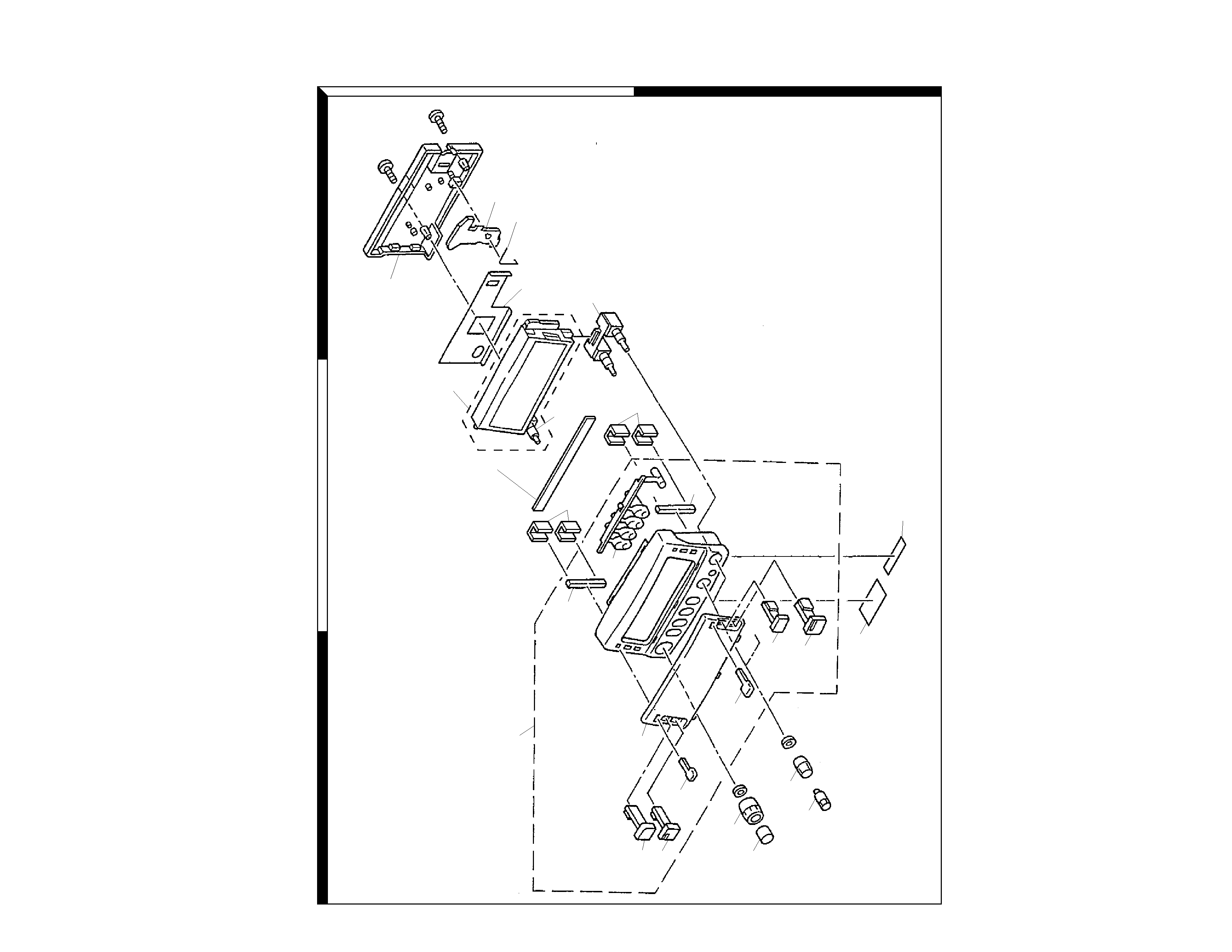
EXPLODED
VIEW
Parts
with
the
exploded
numbers
larger
than
700
are
not
supplied.
S/No. label
B
21
B
9
2
4
10
X57
(C/3)
12
14
14
11
11
3
15
16
16
17
18
23
22
A
A
24
25
19
20
8
1
26