© 2003-9 PRINTED IN JAPAN
B53-0094-00 (N) 1424
HD RADIO TUNER
KTC-HR100
SERVICE MANUAL
HD
R
AD
IO
T
UN
ER
TO
S
LAV
E U
NIT
TO
S
LAV
E U
NIT
TO
C
ON
TR
OL
LE
R
AU
DIO
O
UT
R
L
AN
T
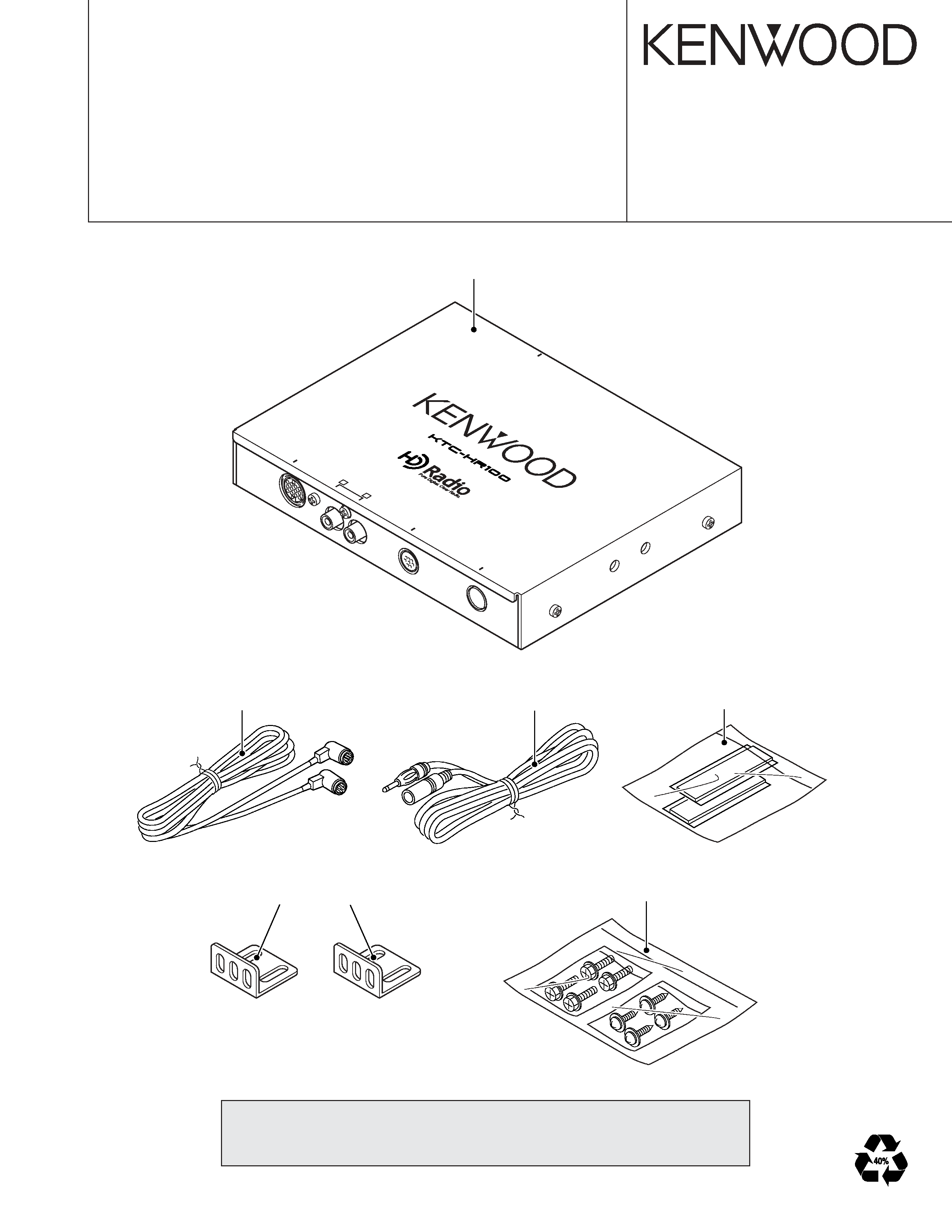
Metallic cabinet
(A01-2830-02)
Cord with plug
(E30-4291-05)
Cord with plug
(E30-4953-05)
Magic tape
(H30-0051-05)
Mounting hardware
(J21-3801-04)
Screw set
(N99-1623-05)
CAUTION (Repair of PROCESSOR UNIT)
You can not repair IC1 (TMSDRI200CGLZ5).
If you can repair those parts please change to PROCESSOR UNIT (X32-5510-10)
KTC-HR100
2
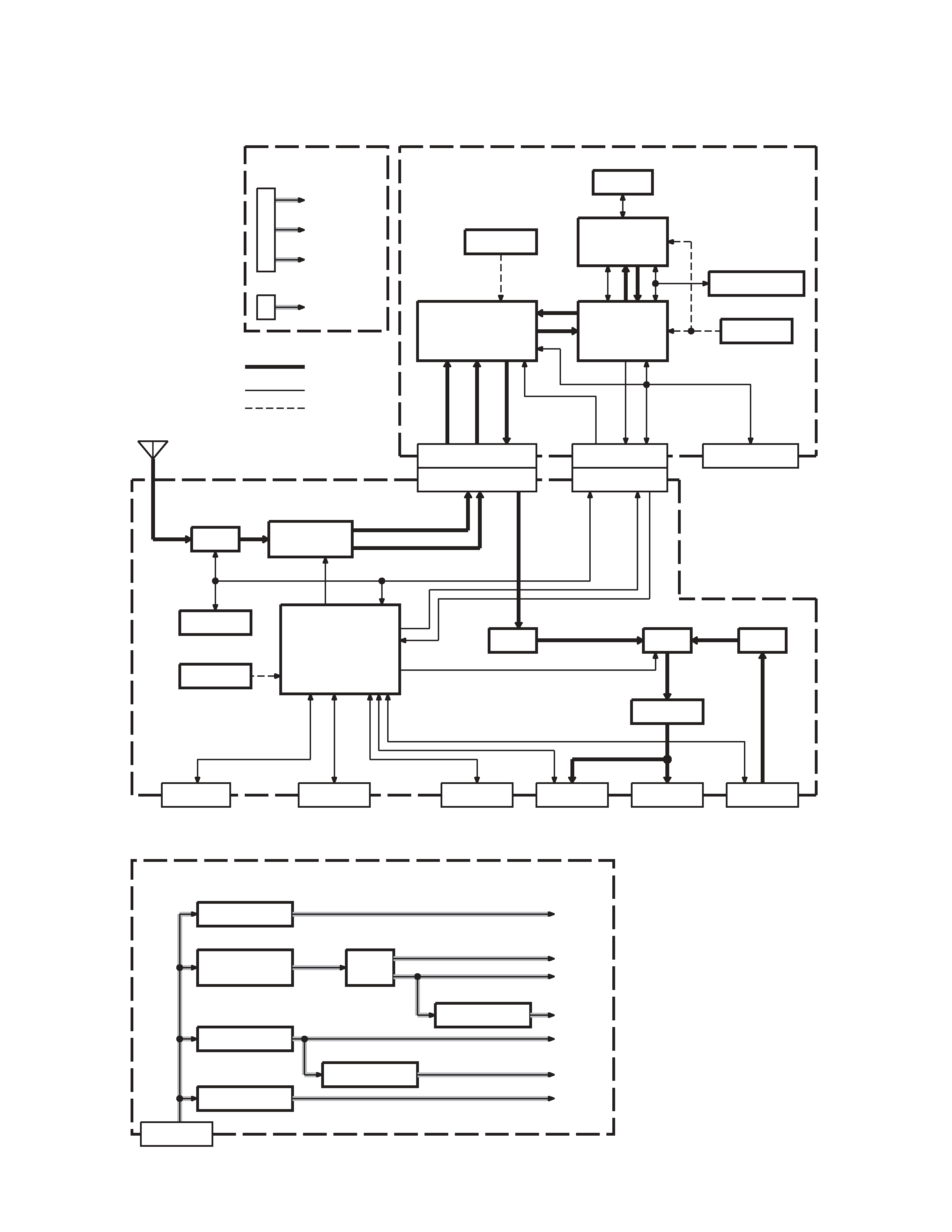
BLOCK DIAGRAM
SDRAM
DSP
FPGA
FLASH ROM
70.56MHz
DEMODULATOR
43.20MHz
IC4
X1
IC1
IC6
IC7
IC2
A1
CN2
CN1
CN5
CN1
CN2
to EXTERNAL UNIT
CN3
CN4
(+1.25V)
3.3V 7724
(+3.3V)
3.3V DSP
(+2.5V)
2.5V FPGA
(+3.3V)
1.25V DSP
F/E
A1
CF1,3
ANTENNA
(OPTION)
SWITCH
FILTERS &
EEPROM
IC15
u-COM
IC11
IC5
AMP
SW
IC2
BUFFER
IC7
AMP
IC3,4
to WRITER
CN6
to HOST PC
CN2
to CONT
J4
to H/U
J2
to CD-CH
RCA
J1
J3
(5L BUS)
(5L BUS)
20.00MHz
X1
REGULATOR
IC1
IC6
IC14
IC17
IC12
Q8,L2,3
IC9
+8V
+3.3V
+2.5V
+1.25V
+8.5V
+5V
REGULATOR
REGULATOR
REGULATOR
REGULATOR
BU5V
DCDC-
CONVERTER
to H/U
J2
SIGNAL
CONTROL
CLOCK
RECEIVER
(ANALOG)
(DIGIT
AL)
A
UDIO
I2C
IF
OUT
IF
OUT
IF OUT(DIGITAL)
IF OUT(ANALOG)
A
UDIO
UA
R
T
I2C
BU
POWER SUPPLY
(X32-5510-10)
(X14-9310-10)
POWER SUPPLY (X14-9310-10)
KTC-HR100
3
DIGITAL TUNER UNIT (X14-9310-10)
Ref. No.
Application/Function
Operation/Condition/Compatibility
IC1
8V regulator
Power supply for audio system
IC2
Analog Switch
Audio Switch
IC3,4
Op-amp
Audio amp 2 for CD-CH signal
IC5
Op-amp
Audio amp 2 for demodulated signal
IC6
DC/DC converter control
Power supply for 3.3,2.5V
IC7
Op-amp
Buffer amp for audio signal
IC8
Op-amp
Convert for audio bias circuit
IC9
1.25V regulator
Power supply for IDM
IC11
µ-com
-
IC12
5V regulator
Power supply for A1 (tuner module)
IC13
Reset IC
-
IC14
5V regulator
Power supply for BU 5V
IC15
1kbit EEPROM
Back-up data memory
IC16
Dual 2 input OR GATE
-
IC17
8.5V regulator
Power supply for A1 (tuner module)
IC18
Op-amp
Comparator for voltage detect
Q1
Mute
For right mute
Q2,3
SW
For main power supply SW
Q4
Mute
For left mute
Q5
SW
For mute
on : mute
Q6,7
SW
For audio source switch
Q8
DC/DC converter
For 3.3,2.5V power supply
Q10
SW
For B.U detect
on : detect
Q11
SW
For B.U detect
on : no-detect
Q12
Inverter
For B.U detect mute
Q14
SW
For 5L CH-CON signal
Q16
SW
For reset
Q17
SW
For CD-CH reset
Q18
Amplifier
IF amp 2
Q19
Amplifier
Signal Amp 2 for AM-IF signal (narrow band)
Q20
Inverter
For AM filter
Q21
Inverter
For FM filter
Q22
Amplifier
Signal Amp for FM-IF signal (wide band)
Q23
Amplifier
Signal Amp for AM-IF signal (wide band)
Q24
Amplifier
Signal Amp for FM-IF signal (narrow band)
Q25
Amplifier
Signal Amp 1 for AM-IF signal (narrow band)
Q26
SW
For FM filter
Q27
5v to/from 3.3v level converter
For I2C data
Q28
5v to 3.3v level converter
For I2C clock
Q29
Amplifier
IF amp 1
Q33
SW
For AM filter
Q35
SW
For B.U detect mute
on : mute
Q36
Level converter
For Blend signal
Q37
SW
For tuner I2C SCL signal
COMPONENTS DESCRIPTION
KTC-HR100
4
Ref. No.
Application/Function
Operation/Condition/Compatibility
Q38
SW
For tuner I2C SDA signal
Q39
SW
For DC-DC controller CS signal
D1
Diode
Protect for a wrong connection
D2,4,6,17,20,21
Zenner diode
Protect for irregularly voltage input
D3,5
Diode
Protect for irregularly voltage input
D7
Diode
Divider for left and right mute circuit
D8
Rectifier diode
For controller voltage
D9,10
OR gate
For mute
D11
Zenner diode
Protect for irregularly voltage input
D13
OR gate
For mute
D14
Zenner diode
Reference voltage for audio bias voltage
D15,16
Schottly barrier diode
For DC/DC converter
D18,19
Diode
Protect for B.U voltage detect circuit
D22,23
Zenner diode
For B.U voltage detect
D25
Diode
Protect for a wrong voltage phenomenon
D26,27,29,30
Zenner diode
Protect for irregularly voltage input
D28
Diode
Reference voltage for regulator
D31
Rectifier diode
For B.U 5V
D32
Diode
Protect for irregularly voltage input
D34
OR gate
For interrupt
D35
Diode
Force for nomal voltage level
D37
OR gate
For mute
D38
Diode
For Controller Power
PROCESSOR UNIT (X32-5510-10)
Ref. No.
Application/Function
Operation/Condition/Compatibility
IC1
DSP
Digital demodulator, Audio decoder
IC2
FPGA
For interface between IC5 and DSP
IC4
Flash Memory
Program data for DSP and FPGA
IC6
64M SDRAM
DSP work area
IC7
Demodulator
AM FM Analog demodulator and Digital Audio interface
Q1
Voltage Regulator
Core voltage supply for IC7 (+2.5V)
D1
LED
This LED is toggled by the DSP software at a rate of approximately (200ms) to indicate
that it is operational.
D2
Diode
Voltage converter for RESET signal
D3
LED
For DC+3.3 [V] power supply check
D4
LED
This LED will blink continuously if the FPGA is configured correctly.
D6
Diode
Voltage protection for DSP
COMPONENTS DESCRIPTION
KTC-HR100
5
MICROCOMPUTER'S TERMINAL DESCRIPTION
MICROCOMPUTER : 70F3030BYGC1R9 (X14 : IC11)
Pin No.
I/O
Pin Name
Function
Processing Operation Description
1O
NC
Not connect
2O
SCK
I2C clock output
3O
RX
UART input
4O
TX
UART output
5O
NC
Not connect
6-
EVDD
Power supply for port
7-
EVSS
Ground for port
8,9
O
NC
Not connect
10
O
MUTE1
5L I/F to H/U
11
O
REQC1
5L I/F to H/U
12
I
DATA_I
Data input from outside driver IC
13
O
DATA_O
Data output to outside driver IC
14
O
LCD_CLK
Clock output to outside driver IC
15
O
LCD_CE
Chip enable for outside driver IC
16
O
LCD_RST
Reset for outside driver IC
17
O
NC
Not connect
18
I
IC/VPP
For write program enable
H : write mode, L : normal
19
O
RELAY
Audio source selection
H : CD-CH, L : HD-RADIO
20
O
A_MUTE
Audio mute output
H : normal, L : mute on
21
O
PON_M
Output for power on main
H : power on, L : power off
22
O
PON_A
Output for power on audio
H : power on, L : power off
23~30
O
NC
Not connect
31
I
RESET
Reset input
H : not reset, L : reset
32
I
-
Un-use (pull down)
33
-
NC
Not connect
34
-
-
Capacitor connection for regulator stabilization
35
-
X2
Resonator connection for main clock
36
I
X1
Resonator connection for main clock
37
-
VSS
Ground
38
-
VDD
Power supply
39~54
O
NC
Not connect
55
-
BVDD
Power supply for BUS interface
56
-
BVSS
Ground for BUS interface
57
O
TU_I2C_SW
Data output for tuner I2C on / off switching
L : off, H : on
58
I
BLEND
Data input for digital / analog switching
L : analog, H : digital
59
O
7724_BLEND
Data output for digital / analog switching
L : analog, H : digital
60
O
IDM_RESET
Reset for IDM
L : reset, H : normal
61
O
FM_ON
Output for FM filter power control
L : filter off, H : filter on
62
O
AM_ON
Output for AM filter power control
L : filter off, H : filter on