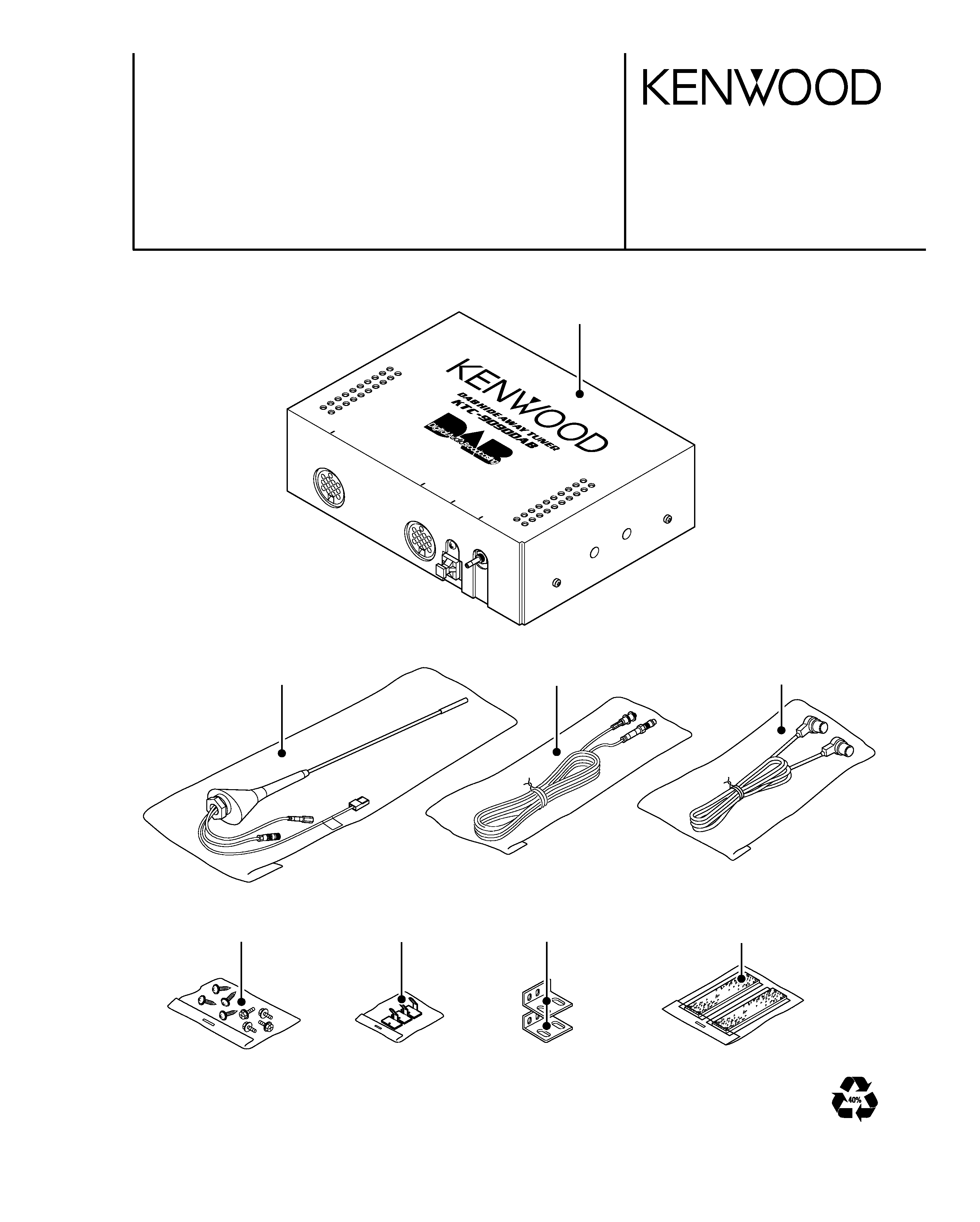
DAB HIDEWAY TUNER
KTC-9090DAB
SERVICE MANUAL
© 2001-7 PRINTED IN KOREA
B51-7833-00 (K) 1927
TO
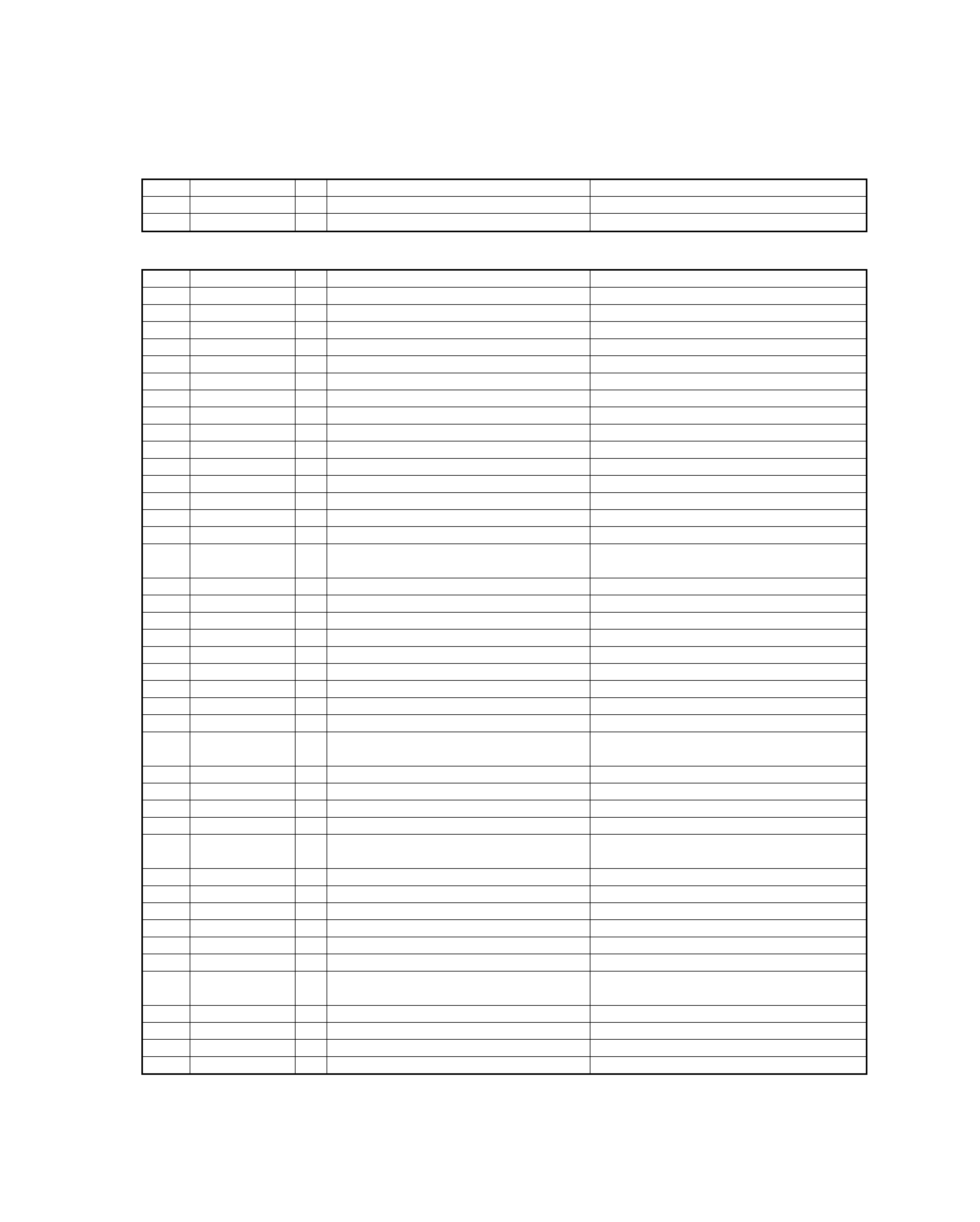
DAB
ANTENNA
RDI
OUTPUT
TO
CHAN
GER
TO
HEAD
UNIT
24bit
D.R
.I.V
.E.
CORD WITH PLUG
(E30-4138-05)
METALLIC CABINET
(A01-2696-12)
ANTENNA ASSY
(T90-0543-05)
ANTENNA ASSY
(T90-0544-05)
SCREW SET
(N99-1623-05)
CLAMPER ASSY
(J11-0647-05)
MOUNTING HARDWARE
(J21-3801-04)x2
MAGIC TAPE
(H30-0051-05)
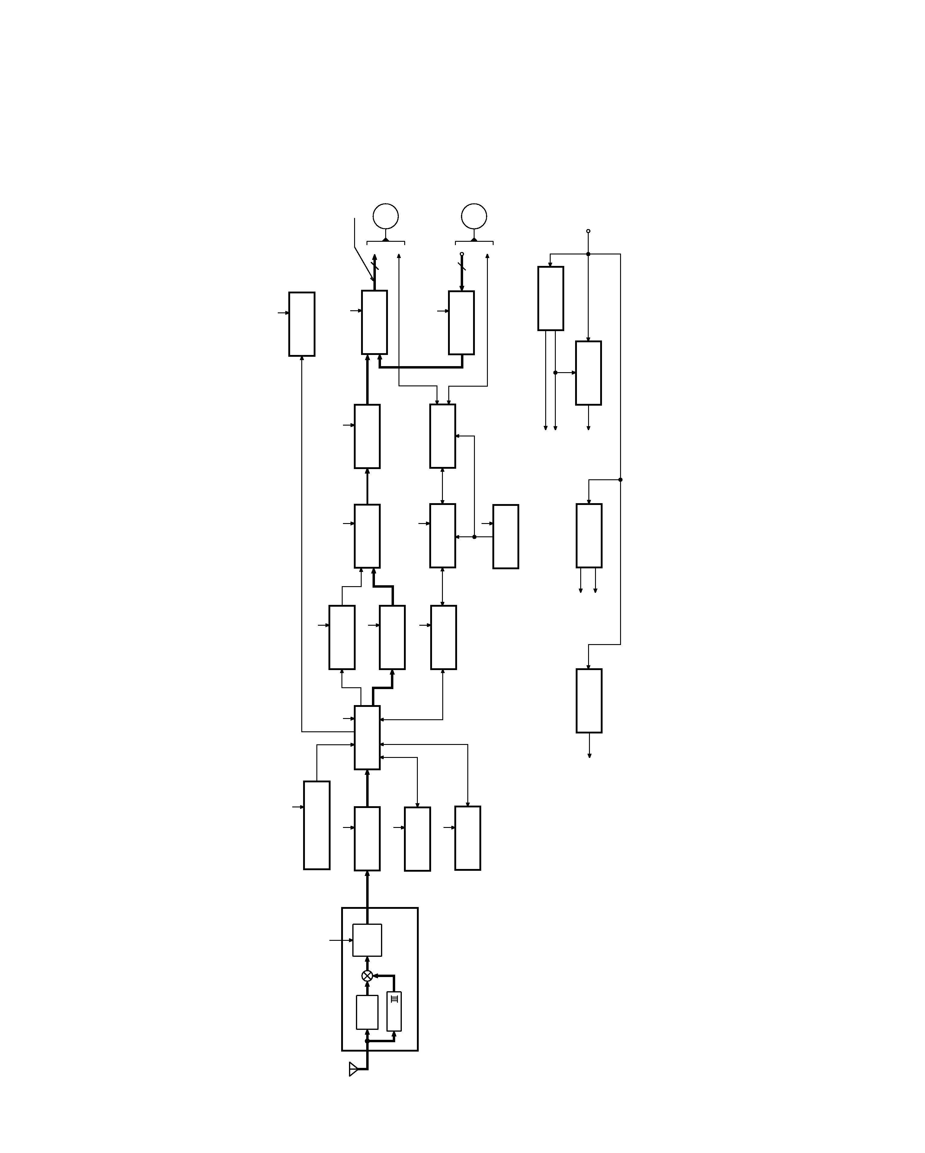
IC2
A/D
CONVERTER
D.R.I.V.E.
IC3
IC6
D/A
CONVERTER
TUNE/
DOWN
ROM
IC18
IC16
CLOCK GENERATOR
24.576MHz
IC13,Q3
VCXO
IF OUT
38.912MHz
600mVp-p
L-BAND
BAND-
CONV.
IF
RF/
DAB
OPT.OUT
A1
X2,
IC14
SRAM
BUFFER
IC11
D.FLIP-FLOP
IC19
3.3V
8.2V
IC12,Q9,18
DC/DC
IC17
5V AVR
OP AMP
SW
AMP
ISOLATION
to HEAD UNIT
from CHANGER
KTC-9090DAB
1100mV
BUFFER
IC20
SYSTEM
IC20
DECODER
PROGRAM
MI-COM
I/F
IC20
IC15
IC1
MI-COM
3.3V
3.3V
3.3V
3.3V
5V
8.2V
8.2V
5V
5V
5V
D5V
D5V
D5V
5V
5V
D5V
8.2V
3.3V
5V AVR
RESET IC
RST
CONVERTER
Q2,19
BUP
BU DETECT
BUPRF
RF DETECT
BU
L,R
L,R
KTC-9090DAB
2
BLOCK
DIAGRAM
Ref.No. Component Name
Application/Function
Operation/Condition/Compatibility
IC1
PST9130NR
Reset IC
When BU 5V voltage is less than 3.0V, IC outputs Lo.
IC2
ADS900E
A/D converter
IF base-band output conversion
IC3
KAN06
D.R.I.V.E. IC
IC4
M30625MGA317GP System MI-COM
IC5
BA3129F
SW OP AMP
Audio output selector between DAB and Changer
IC6
AK4393
D/A converter
IC8
NJM4565M-TE2
OP AMP
Operational reference voltage buffer for IC5 and IC21
IC10
UPD78058GCB82T IF MI-COM
Communication interface between DAB, Changer and H/U
IC11
HD74HCT244T
3-state buffer
Data output buffer and logic level conversion from IC16 to IC3,
IC4 and A1
IC12
MB3778PF
DC/DC converter control IC
DC/DC chopper control for 8.2V and 3.3V power lines
IC13
TC7SHU04F
Inverter
Wave shaping and clock generator for Back-end decoder
IC14
HM62W8511HJ15
SRAM
Data memory for Back-end decoder and System MI-COM
IC15
TA78DL05F
5V AVR
Power supply for System MI-COM, IF MI-COM, 3-state buffer
and DC/DC converter control IC
IC16
U2739M-B
Back-end decoder
I/Q detector, FFT, Channel decoder, MPEG decoder
IC17
TA78L05F
5V AVR
Power supply for D.R.I.V.E. IC, D/A converter, D flip-flop and
optical transmitter
IC18
27LV256A12RD01
ROM
Program ROM for Back-end decoder
IC19
TC74HC74AF
D flip-flop
1/2Fs, Clock generator for D.R.I.V.E. IC
IC20
TC7WT241FU
3-state buffer
Data input/output and logic level conversion between IC4 and
IC16
IC21
NJM4565M-TE2
OP AMP
Isolation amplifier for CH audio outputs
Q1
DTC124EUA
RESET SW
When H/U's RESET becomes Hi, Q1is turned on and System
reset is working.
Q2
DTC144EUA
RF power down detection SW
When BACKUP voltage is less than 9.0V, a base goes Lo, and
Q2 is turned off.
Q3
2SC4097
Master clock buffer
Driver of low pass filter
Q4
2SD1757K
Mute SW (R Ch)
When a base becomes Hi, audio mute is working.
Q5
2SD1757K
Mute SW (L Ch)
Q6
DTC144EUA
CH CON SW
While CH CON or CH-CON2 mode is selected, a base
becomes Hi and Q6 is turned on.
Q9
2SA2006
DC/DC chopper
DC/DC chopper for 8.2V power line
Q10
DTC124EUA
Audio output select SW
While DAB output is selected, a base becomes Lo and Q10 is
turned off.
Q7
DTC144EUA
When RF power line down has detected, Q13 is turned on.
Q12
DTA124EUA
Mute driver
While Q7 or Q13 is turned on, Q12 is turned on and Audio
Mute is working.
Q13
DTC124EUA
When CH MUTE 1 becomes Hi, Q7 is turned on.
Q18
2SA2006
DC/DC chopper
DC/DC chopper for 3.3V power line
While BACKUP is applied, a base goes Hi, and Q19 is turned on.
Q19
DTC124EUA
BU detection SW
When momentary power down has detected, a base goes Lo,
and Q19 is turned off.
DIGITAL/ANALOGUE CONVERTER UNIT(X14-6522-70)
KTC-9090DAB
3
COMPONENT DESCRIPTION
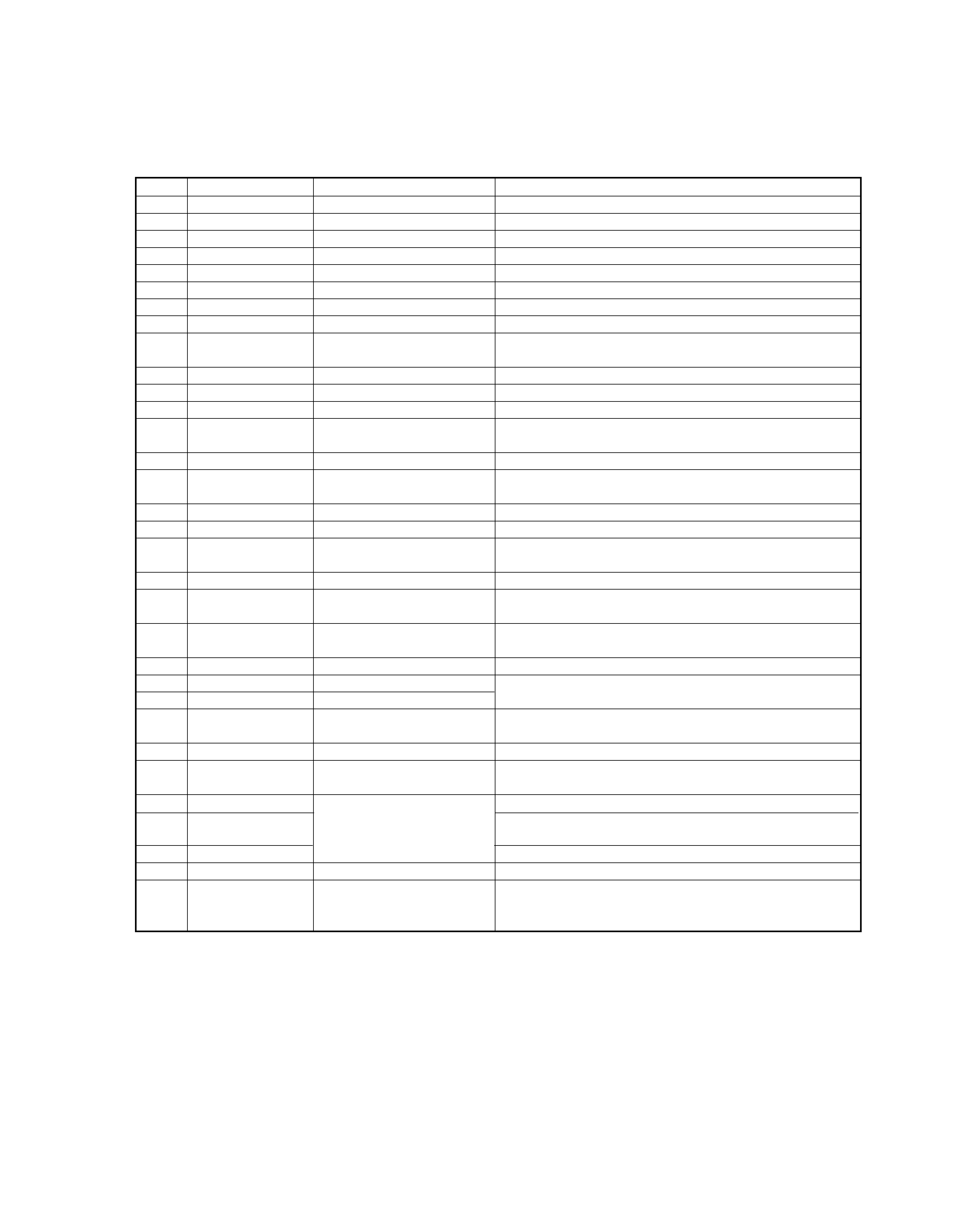
Pin No.
Pin Name
I/O
Description
Processing Operation
1
MC CLK
O
Bus clock to IC16
2
MCM TRIGGER
I
Data trigger from IC16
Hi: Trigger on, Lo: Trigger off
3-5
O
Not used(N.C.)
6
VSS
I
Connected to CN1(pull down to GND lines.)
7,8
O
Not used(N.C.)
9
RESET
I
System reset terminal
Lo: System reset
10
XOUT
O
Main clock resonator connection terminal
11
VSS
-
Ground connection terminal
Connected to GND lines.
12
XIN
I
Main clock resonator connection terminal
13
VCC
-
Positive power supply connection terminal
Connected to 5V lines.
14
VCC
I
Connected to CN1(pull up to 5V lines.)
15
O
Not used(N.C.)
16
REQH
I
Communication request from IF MI-COM
Lo: Communication requested
17
CHCON
I
Changer control input
Hi: Standby, Lo: Operation
18,19
O
Not used(N.C.)
20
CH MUTE
O
Audio mute request to IF MI-COM
Hi: Audio mute requested
21-23
O
Not used(N.C.)
24
BUS DIN
I
Connected to CN1
25
BUS DOUT
O
Connected to CN1
26
BUS SCK
I
Connected to CN1
27
BUS RST
I
Connected to CN1
28
DATAC
O
Data output to IF MI-COM
29
DATAH
I
Data input from IF MI-COM
30
MCLK
I
Communication clock input from IF MI-COM
31
REQC
O
Communication request to IF MI-COM
Lo: Communication requested
32,33
O
Not used(N.C.)
34
VSS
I
Connected to CN1(pull down to GND lines.)
35,36
O
Not used(N.C.)
37
BUP
I
Momentary power down detection input
Hi: When momentary power down detected or
BU OFF, Lo: BU ON
38
BUPRF
I
RF power down detection input
Hi: When BU voltage is less than 9.0V.
39
VCC
I
Connected to CN1(pull up to 5V lines.)
40
E CON
O
Peripheral circuit power on/off output
Hi: 3.3V and 8.2V AVR power on
41
I2C DATA
O
Data output to FE
42
I2C CLK
O
Clock output to FE
43-60
Not used(N.C.)
61
RS U2739M
O
Reset output to IC16
Lo: Reset
62
MC MODE
O
Bus mode with IC16
63
MC DATSEL
O
Bus data direction select terminal
Hi: from IC16 to MI-com, Lo: from MI-COM to
IC16
64,65
O
Not used(N.C.)
66
DAC RST
O
Reset output to DAC
Lo: Reset
67
HALF SW
O
Half rate sampling audio select SW
Hi: fs=24kHz, Lo: fs=48kHz
68
DAC CS
O
Data latch output to DAC
69
DAC SCLK
O
Serial clock output to DAC
70
DAC SDATA
O
Serial data output to DAC
71
O
Not used(N.C.)
72
SEL3
I
Destination select terminal 3
Not used(pull down to GND lines.)
73
SEL2
I
Destination select terminal 2
Hi: without 5L interface MI-COM
74
SEL1
I
Destination select terminal 1
Hi: Canada, Lo: Europe
75
VSS
-
A/D converter ground connection terminal
Connected to GND lines.
76
SEL0
I
Destination select terminal 0
Not used(pull down to GND lines.)
77
VREF
-
A/D converter reference voltage input
Connected to 5V lines.
78
AVCC
-
A/D converter positive power supply
Connected to 5V lines.
connection terminal
IC4 (DIGITAL/ANALOGUE CONVERTER UNIT : X14-6522-70)
KTC-9090DAB
4
MICRO COMPUTER'S TERMINAL DESCRIPTION
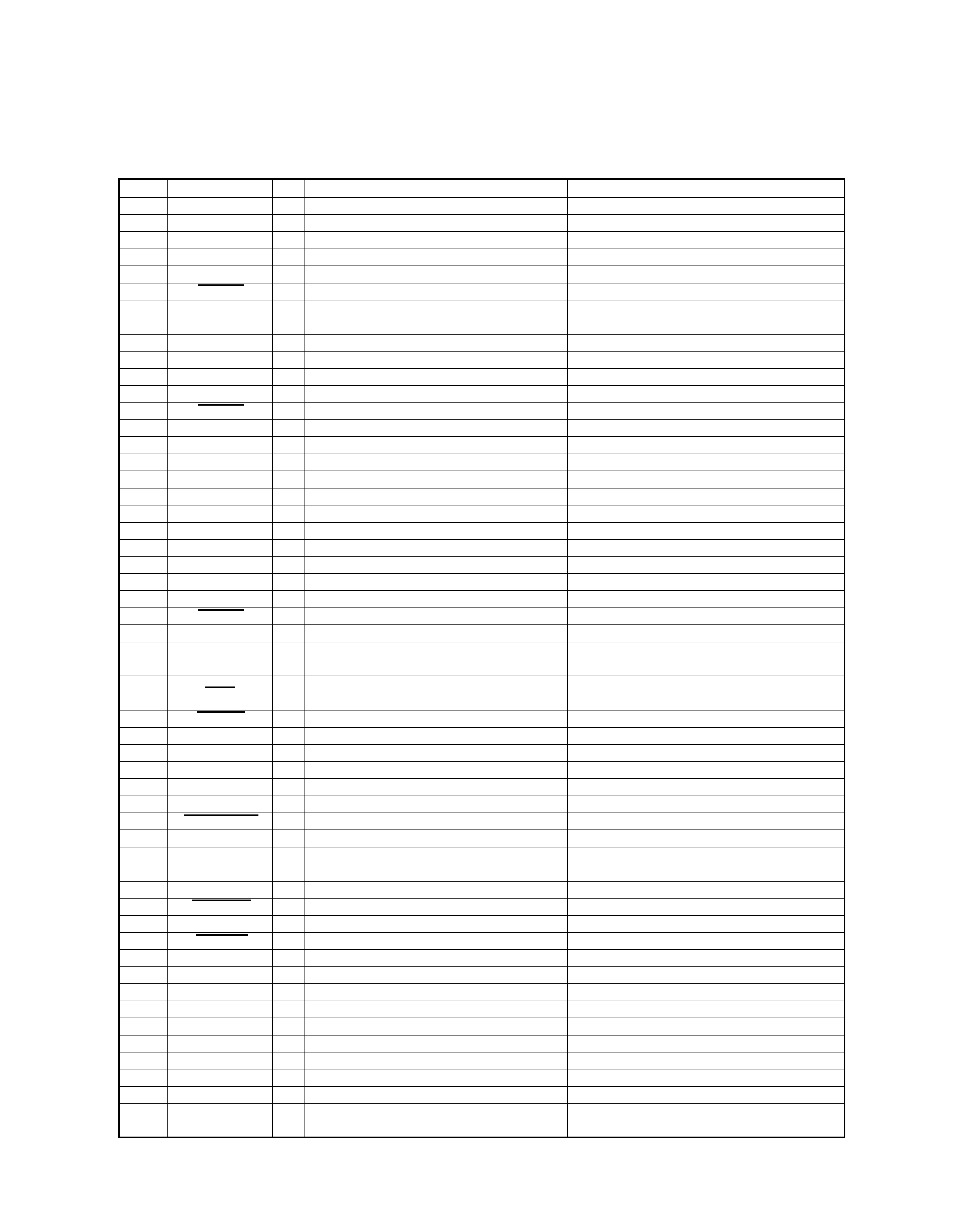
KTC-9090DAB
5
Pin No.
Pin Name
I/O
Description
Processing Operation
1 - 3
NC
O
Not used(N.C.)
4
AVSS
-
A/D converter ground terminal
5
RST OUT
O
Reset output to changer
Hi: Changer reset
6
REQH1
O
Communication request output to DAB
Lo: Communication requested
7
AVREF1
I
D/A converter reference voltage input
Connected to 5V lines.
8
DATAC1
I
Data input from DAB
9
DATAH1
O
Data output to DAB
10
HCLK1
I/O Communication clock input/output with DAB
11
DATAH0
I
Data input from H/U
12
DATAC0
O
Data output to H/U
13
HCLK0
I/O Communication clock input/output with H/U
14
REQC0
O
Communication request output to H/U
Lo: Communication requested
15
REQH2
O
Communication request output to changer
Lo: Communication requested
16
DATAC2
I
Data input from changer
17
DATAH2
O
Data output to changer
18
HCLK2
I/O
Communication clock input/output with
changer
19
CHCON01
O
Control output to DAB
Hi: DAB operation
20
CHCON02
O
Control output to changer
Hi: Changer operation
21
RELAY1
O
Relay1 Control output
Not used(N.C.)
22
RELAY2
O
Relay2 Control output
Hi: Changer outputs, Lo: DAB outputs
23-32
NC
O
Not used(N.C.)
33
VSS
-
Ground connection terminal
Connected to GND lines.
34-59
NC
O
Not used(N.C.)
60
RESET
I
Reset input
Lo: System reset
61
REQC2
I
Communication request input from changer
Lo: Communication requested
62
BUDET
I
Momentary power down detection input
Hi: When momentary power down detected or
BU OFF, Lo: BU ON
63
AUX SW
Auxiliary input switch
Not used(pull down to GND lines.)
64
REQH0
I
Communication request input form H/U
Lo: Communication requested
65
REQC1
I
Communication request input form DAB
Lo: Communication requested
66
CHCON1
I
Changer control input from H/U
Lo: DAB Control mode
67
COMMSW
I
5-line communication old/new switch
Hi: New communication, Lo: Old
communication
68
VDD
-
Positive power supply connection terminal
Connected to 5V lines.
69
X2
-
Main clock resonator connection terminal 2
70
X1
I
Main clock resonator connection terminal 1
71
IC
-
IC Internal connection terminal
Connected to GND lines.
72
NC
O
Not used(N.C.)
73
CHCON2
I
Changer control input from H/U
Lo: Changer control mode
74
AVDD
-
A/D converter positive power supply
Connected to 5V lines.
connection terminal
75
AVREF0
I
A/D converter reference voltage input
Not used(connected to GND lines.)
76
NC
O
Not used(N.C.)
77
AUX TYPE
O
Not used(pull down to GND lines.)
78-80
NC
O
Not used(N.C.)
Pin No.
Pin Name
I/O
Description
Processing Operation
79
MC DATI
I
Data input from IC16
80
MC DAT0
O
Data output to IC16
IC10 (DIGITAL/ANALOGUE CONVERTER UNIT : X14-6522-70)
MICRO COMPUTER'S TERMINAL DESCRIPTION
IC4 (DIGITAL/ANALOGUE CONVERTER UNIT : X14-6522-70)