SRC
KRC-435
47Wx4
DOLBY B NR
SCAN
B.S/RDM
REP
MTL/M.RDM
B NR
NAME
DISP
AUD
MENU
PROG
DAB
OFF
LOUD
AME
AUTO
© 2001-12 PRINTED IN JAPAN
B51-7877-00 (S) 1757
SERVICE MANUAL
CASSETTE RECEIVER
KRC-435/665
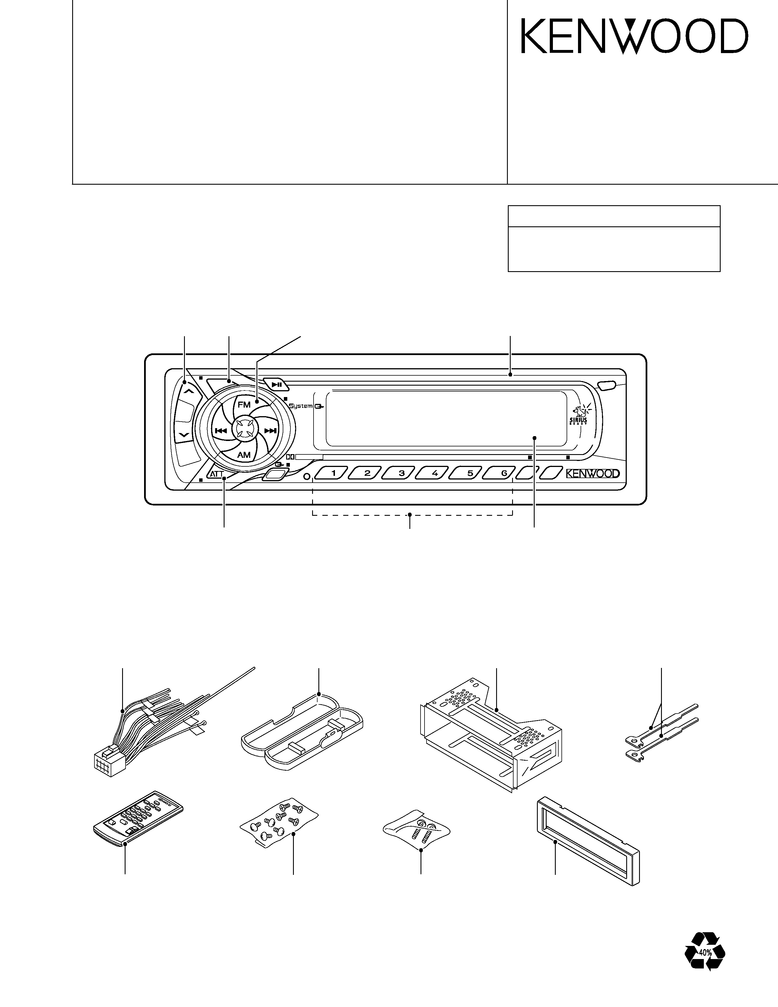
Front glass
(B10-4188-01)
Knob(SRC)
(K25-1410-03)
q KRC-435
Lever
(D10-4589-04)
DC cord
(E30-4784-05)
MECHANISM EXTENSION CORD
W05-0477-00 (7P)
W05-0609-00 (10P)
Refer to the PARTS LIST
Plastic cabinet assy
(A02-1486-13)
Mounting hardware assy
(J21-9716-03)
Screw set
(N99-1719-05)
Remote controller assy RC-410
(A70-2025-05)
Screw set
(N99-1656-05)
Escutcheon
(B07-3060-02)
Knob(VOL)
(K25-1414-03)
Panel assy
(A64-2610-02)
Knob(1-6)
(K25-1409-03)
Knob(FM,AM)
(K25-1412-03)
Knob(ATT)
(K25-1411-03)
KRC-435/665
2
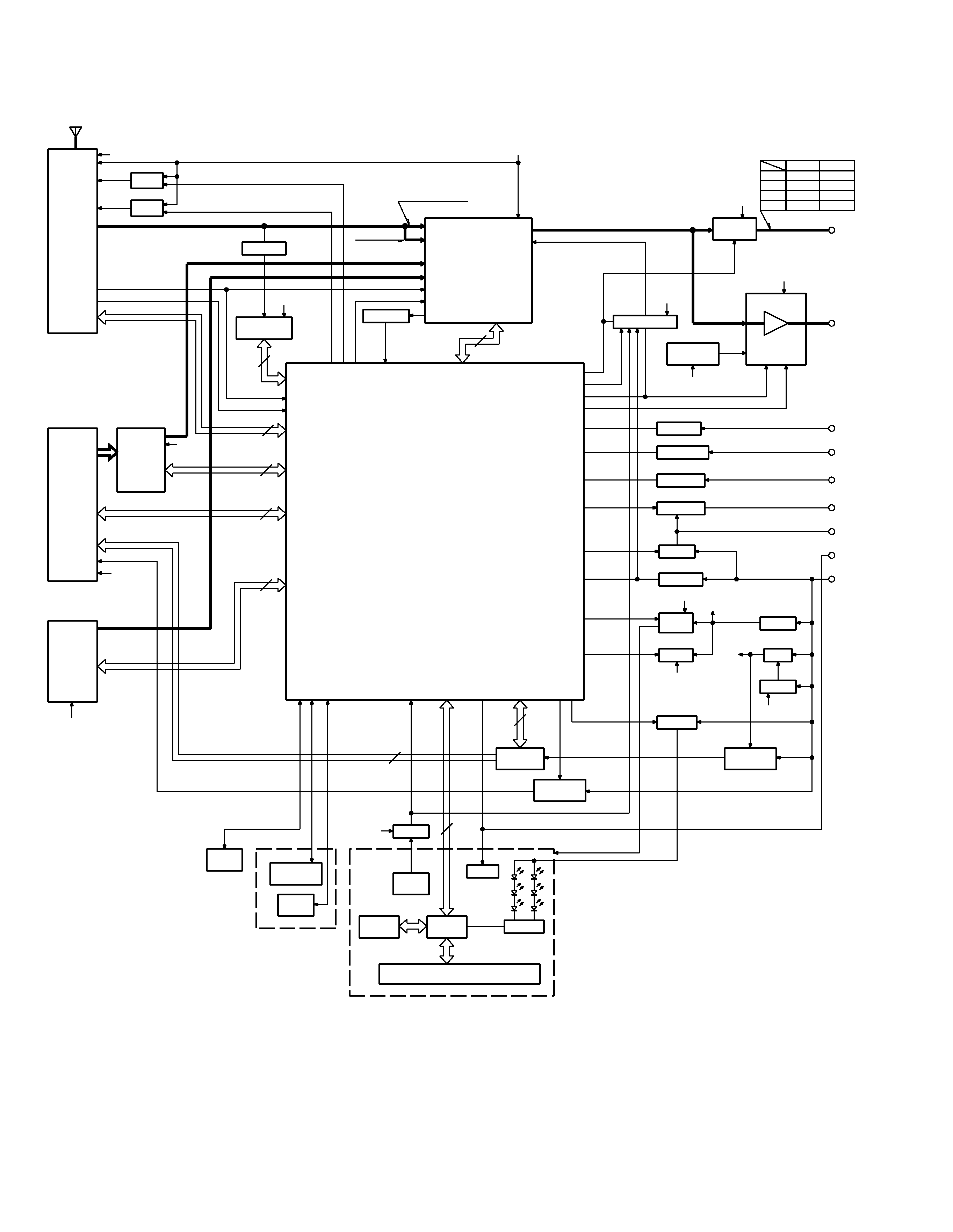
BLOCK DIAGRAM
DIMMER
TEL MUTE
ACC
ANT CON
P CON
BACK UP
WIRED
FM+B
BUFFER
BUFFER
DECODER
RDS
IC7
IC2
E-VOL
MPX
N.C.
AM+B
SYSTEM u-COM
IC1
KEY
MATRIX
RESET
SW
LCD
DRIVER
G/R SW
RESET
IC8
IC1
DRIVER
SUB MOT
IC10
MAIN MOT
AVR
VOLTAGE
LIMITTER
ILL AVR
A 8V
Q16,17
SW14V
DIMMER
ACC DET
TEL MUTE
P CON
B.U DET
ANT CON
SW5V
B.U.5V
P-5V
Q11,12
POWER IC
THERMO
PROTECT
IC4
IC3
MUTE LOGIC
DRIVER
MUTE
Q1-4
SP OUT
1.8V
LCD
ANT.
Q31
Q61
Q39
Q32,33
Q34-36
Q38
Q13
Q14,15
Q23
Q72
Q18,19
Q3,4
Q44
Q55
Q54
Q52
REMO
REMO
PRE OUT
PANEL
DET
EJECT ILL
DSI
KEY
EJECT
TH1
IC2
S1
ED1
IC9
251mV (E TYPE)
460mV (K TYPE)
FM :
1200mV
388mV
AM : 230mV
TUNER
MECHA
CD-CHANGER
MD-CHANGER
(X16- )
DOLBY EQ
CASSETTE
AUDIO
S-METER
PLL DATA
PLL CLK
SW 5V
FM
AM
TAPE
CHANGER
S METER
QUAL
SD
A
SCK
S MUTE
A 8V
SUB-
MOT+B
SUB+
PACK IN
F/R
T-END
STBY
HEAD COM
HEAD L
HEAD R
MODE
SUB
+
RCLK
QUAL
RDATA
S METER
IFC
PLL DATA
PLL CLK
MUSIC
MS CONT
F/R
T-MODE
PACK IN
M-STBY
T-END
METAL
EQ-MUTE
DATA C
CH RST
CH MUTE
DOLBY
DATA H
CH CON
CH CLK
REQ H
REQ C
SUB
-
RESET
M
OTO
R
ILL
ON
AM+B
FM+B
SCK
SD
A
PRE MUTE
MUTE
BEEP
P MUTE
ACC DET
PHONE
DIMMER
P CON
P-5V
P ON
ANT CONT
B.U DET
SW 5V
3
2
5
CH MUTE
CH RST
DATA H
DATA C
CH CON
REQ C
CH CLK
REQ H
BACK UP
8
SW 5V
2
B.U. 5V
2
SUB-
SUB+
MOT+B
A 8V
PAN 5V
B.U. 5V
SW 5V
MUTE
A
UX
IN
BACK UP
SW 5V
B.U. 5V
B.U. 5V
CH
FM
1800mV
TAPE
AM
3600mV
855mV
1372mV
600mV
3600mV
1800mV
E TYPE
K TYPE
1800mV
NOISE
AFS
AFS
IFC OUT
2
SW 5V
5
MS MODE
TAPE SW
NR SW
MUTE SW
MS OUT
A 8V
REMO
L
D
ATA
S
L
CLK
DIM
CON
L
CE
L
D
ATA
L
L-CLK
P
ANEL-DET
EJECT
-ILL/DSI
EJECT
MODE+B
6
KRC-435/665
3
COMPONENT DESCRIPTION
q SYNTHESIZER UNIT (X14-68XX-XX)
Component
Purpose · Function
Operation · Conditions · Compatibility
IC1
SYSTEM µ-COM
IC2
E-VOL, N.C. NPX
IC3
Mute logic circuit
4 input NOR gate x 4
IC4
Power IC
IC7
RDS Decoder
IC8
Reset IC
"L" detection voltage: 3.0 V or less
IC9
Equalizer amplifier
DOLBY B
IC10
Sub motor driver
IC11
EEPROM
Q1
Audio mute SW
Front L-channel is muted when base goes "H".
Q2
Audio mute SW
Front R-channel is muted when base goes "H".
Q3
Audio mute SW
Rear L-channel is muted when base goes "H".
Q4
Audio mute SW
Rear R-channel is muted when base goes "H".
Q11,Q12
B.U. 5V AVR
Darlington connection
Q13
SW 5V
ON when base goes "L".
Q14,Q15
SW 14V
Audio 8V ON/OFF SW
Q15 is turnd ON when Q14's base goes "H".
Q16,Q17
AUDIO 8V AVR
Darlington connection
Q18,Q19
Main motor SW
Q19 is turnd ON when Q18's base goes "H".
Q20,Q21
ILL power ON/OFF SW
Q21 is turnd ON when Q20's base goes "H".
Q23
ILL AVR
Inverted darlington connection
Q31
Dimmer control SW
Small light detection when base goes "H".
Q32,Q33
Power antenna SW
Q33 is turnd ON when Q32's base goes "H".
Q34,Q37
Power control SW
Q34 is turnd ON when Q37's base goes "H".
Power control circuit
When the output voltage decrease is detected, Q37 is turned off to protect the output.
Q35,Q36
output protection
When the power control switch is turned on, Q35 protects the system from
misoperation.
Q38
B.U detection
"L" when B.U is present.
"H" when B.U is absent or when momentary power down detction.
Q39
ACC detection
"L" when ACC is present.
Q42
Mute driver
For driving the audio mute switch.
ON when the base goes "L".
Q43
MUTE SW for E-VOL.
Turns on when base goes "L" and E-VOL is muted.
Q44
Noise buffer
Q51,Q52
FM+B SW
Q52 is turnd ON when Q51s base goes "H".
Q53,Q54
AM+B SW
Q54 is turnd ON when Q53s base goes "H".
Q55
Composite signal buffer
Q61
PANEL 5V SW
ON when the base goes "L".
Q71
MSTC SW
ON when the base goes "H".
Q72
Sub motor AVR
7.3V output when AUDIO 8V is turned on.
Q82
EJECT ILL/DSI SW
ON when the base goes "L".
q SWITCH UNIT (X16-16XX-XX)
Component
Purpose · Function
Operation · Conditions · Compatibility
IC1
LCD driver
IC2
Remocon IC
Q1
Key scan start SW
ON when the base goes "L".
Q2
Remocon IC VDD supply SW
Supply of Remocon IC VDD when the base goes "L".
KRC-435/665
4
q IC1(SYNTHESIZE UNIT : X14-68XX-XX)
Pin No.
Pin Name
I/O
Description
Processing Operation
1
TYPE 1
I
Destination type selection port
2
TYPE 2
I
Destination type selection port
3
IFC
I
F/E IFC OUT input terminal
H: Station exists
Vth: 2.5V
4
AVSS
-
A/D,D/A converter ground connection terminal
Connected to GND lines.
5
IC2-TYPE 1
I
Maket/genuine select (Noise cancel)
L: Maket
H: genuine
6
PANEL-DET
I
Panel detection
L: Panel exists
H: Panel does not exists
7
AVREF1
I
D/A converter reference voltage input terminal
Connecting to BU5V
8
CH-DATAC
I
Data input from changers
9
CH-DATAH
O
Data output to changers
Last maintenace
10
CH-CLK
I/O Clock input/output with changers
input
11
L-DATAL
I
Data input from the LCD driver IC
Communication speed 600kHz (max)
12
L-DATAS
O
Data output to the LCD driver IC
Communication speed 1.2MHz (max)
L: Panel detached
13
L-CLK
O
Clock output to the LCD driver IC
L: Panel detachd
14
L-CE
O
LCD driver chip enable
H: Driver select
L: Not select
15
BEEP
O
BEEP sound output
16
PLL-DATA
I/O Tuner (01ST) data input/output
Last maintenace
17
FLIP-DET
I
Panel detach detection
L: Panel attached
H: Panel detached
18
PLL CLK
O
Tuner (01ST) clock input/output
19
N.C.
O
Not used
20
EJECT ILL/DSI
O
EJECT ILL KEY & DSI output
L: Light ON
H: Light OFF
21
L-RST
O
Reset output to the LCD driver IC
L: Reset ON H: Reset OFF
22
PAN 5V
I/O Panel 5V control terminal
L: ON (Panel exists & ACC ON)
H: OFF (Panel does not exists or ACC OFF)
23
R-DATA
I
Data input from the RDS decoder IC
24
R-QUAL
I
Quality input from the RDS decoder IC
25
SUB (-)
O
Sub motor output (-)
26
SUB (+)
O
Sub motor output (+)
27
FWD/rev
I
Cassette tape running direction detection
H: FWD
L: REV
28
MS-CONT
O
ADV sensitivity control
H: PLAY
L: FF/REV
29
metal
O
NORMAL/METAL change
H: NORMAL L: METAL
30
EQ-MUTE
O
EQ-MUTE change
H: ON
L: OFF
31
DOLBY
O
Dolby ON/OFF
H: ON
L: OFF
32
music
I
Casstet music space detection
H: Music does not exists
L: Music exist
33
VSS1
-
GND
34
IC2 TYPE 0
I
Maket/genuine select 0 (ROLL-OFF)
L: Market
L: Genuine 0
35
AM+B
O
AM power supply terminal
H: During AM reception
36
FM+B
O
FM power supply terminal
H: During FM reception if with RDS
37
AFS
O
Noise detection time constant switching terminal
Hi: During FM reception, Lo: During FM seek or
AF search
38
IC2-CLK
O
IC2 clock output
39
IC2-DATA
I/O IC2 data input/output
40
EEPROM DET
I
EEPROM detection terminal
H: EEPROM exist
L: EEPROM does not exists
41
P-MUTE
O
Power IC mute control output
H: Mute OFF
L: Mute ON, PowerOFF, All OFF, TEL Mute
42
P-STBY
O
Power IC standby control output
L: Power IC OFF, All OFF mode
H: Power IC ON
43
MUTE
O
IC2 mute control output
H: Mute ON
L: Mute OFF
44
PRE MUTE
O
Pre-out mute control
L: Momentary power down, Reset
45
DIMMER-CON
O
Dimmer Control
Control with pulse output
H: Power ON
L: Power OFF
46
BU-DET
I
Momentary power down detection input
H :BU OFF
L : BU ON
47
ACC-DET
I
ACC detection input
L: ACC ON
H: ACC OFF
48
dimmer
I
Small lights detection input
L: ON
H: OFF
49
REMO
I
Data input from the remote control light sensor
50
ANT-CON
O
Antenna control output
H: TUNER, TI
MICROCOMPUTER'S TERMINAL DESCRIPTION
KRC-435/665
5
MICROCOMPUTER'S TERMINAL DESCRIPTION
Pin No.
Pin Name
I/O
Description
Processing Operation
51
P-CON
O
Power control output
H: Power ON L: Power OFF
52
CH-RECH
O
Request output to changers
L: Request
53
CH-RST
O
Reset output to changers
L: Normally
54
CH-MUTE
I
Mute request from changers
H: ON
L: OFF
55
CH-CON
O
Changer control
H: ON
L: OFF
56
P-ON
I/O SW 5V control output
H: OFF
L: ON
57
MOTOR
O
Main motor output
H: ON
L: OFF
58
M-STBY
I
Cassette standby detection
H: STBY
59
T-END
I
Tape end detection
H: Tape play L: Tape end
60
reset
I
Reset input terminal
L: System reset
H: Normally
61
eject
I
Eject key detection
H: OFF
L: ON
62
CH-REQC
I
Request input from changers
H: OFF
L: ON
63
ILL ON
O
Illumination output terminal
H: ON
L: OFF
89
KEY-REQ
I
Panel key interrupt input
L: Key input exist
65
R-CLK
I
Clock input from the RDS decoder IC
66
PACK-IN
I
Cassette pack-in detection
H: Pack-in
67
VSS0
-
GND (port)
68
VDD1
-
Positive power supply
69
X2
-
Main clock output (12MHz)
70
X1
I
Main clock input
71
TEST
I
Program power supply (Mask: Test terminal)
72
XT2
-
Sub clock output (32.768MHz)
73
XT1
I
Sub clock input
74
VDD0
-
Positive power supply (port)
75
AVDD
I
A/D port reference voltage input
76
PHONE
I
Phone detection terminal
Less than 1V: TEL mute
More than 2.5V: NAVI mute
77
T-MODE
I
Tape mode detection
Vth=2.5V
78
S-METTER
I
S-meter input from F/E
79
NOISE
I
FM noise detection input
80
TYPE 0
I
Destination type selection terminal