© 2004-1 PRINTED IN JAPAN
B53-0120-00 (N) 1839
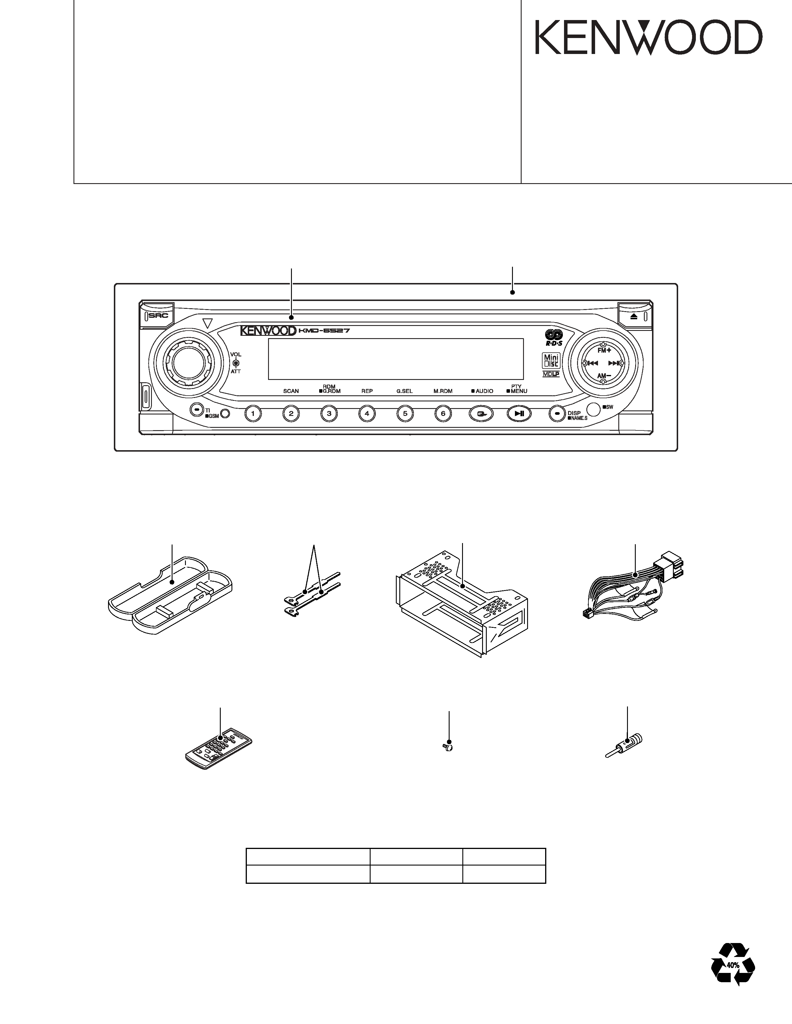
MD RECEIVER
KMD-6527
SERVICE MANUAL
Plastic cabinet assy
(A02-2732-03)
Lever
(D10-4589-04) x2
Screw
(N09-6212-05)
Mounting hardware assy
(J21-9716-03)
Panel assy
(A64-3220-02)
MODEL
TDF PANEL No. TDF NAME
KMD-6527
Y33-1990-64
TDF-6527
TDF PANEL INFORMATION
Escutcheon
(B07-3083-02)
DC cord
(E30-6063-15)
Antenna adaptor
(T90-0523-05)
Remote controller assy (RC-420)
(A70-2055-05)
KMD-6527
2
BU
PON5
BU
SW5
BU5
SW3
F+/F-
FL+B
RDS
F/E
LX-BUS
DISP
OPEL-
AUX
MD-DET
PANEL-
MECHA
MDS-3200
MD
INGAIN
STD
MAIN
SUB
PHONE
/NAVI
INPUT
-MPX
INGAIN
+
TREBLE
BASS
VOLUME
MID
0
AUTOZER
OUT-SEL
SOFT
MUTE
FRONT
REAR
NF/R
FRONT
REAR
NF
FADER
DC
DET
OFFSET
E'S LIGHT
C/R : DISCREET
E-VOL
PW-IC
PRE-OUT
PRE-OUT
SP-OUT
MUTE
MUTE
ACC
ACC-DET
REG.
ANT-SW
REG.
P-CON
REG.
BU
SW
BU5V
SERVO
MD
REG.
DC/DC
SW11V
FL
F+/F-
FL +B
SW5V
MECHA
PANEL
DRIVER+B
BU5V
ILL+B
A8V
BU-DET
ANT-CON
SYSTEM u-COM
REMO
KEY
MATRIX
u-COM
PANEL
SHIFT
LEVEL
FL
SW
IC4
Q49,50
Q47,48
Q36
SW REG.
Q27
Q25
Q10,11
IC13
IC19
Q3
Q1,2
A1
IC20
Q15,16
IC7
Q35
IC3,Q8
Q3
ED1
IC1
IC3
IC1
A2
IC12
IC2
Q58,59
MUTE
MUTE
Q56,57
METER
LEVEL
IC14
MD SERVO
BU5
MPX
AUX
CH
CD
NAVI
CH/AUX
AC
IN0
AC
IN1
AC
IN2
AC
IN3
AC
OUT
SUB
IN1 : HPF
IN2 : 2ZONE
IN3 : LPF
ACIN 3+LPF
: FREE ONLY
HPF
NF
FR
NO HPF
F/R/NF
DC
MUTE L/R
FRONT
MUTE L/R
REAR/NF
R/L
R/R
F/L
F/R
MONO 2ch
PON
P-CON
PON
PON CD/MD
PON
A
UDIO
PWIC
POWER
DET
PON ILL
TYPE
P
ANEL
FL+B
2ZONE
(X34- )
(X16-252)
(X16-251)
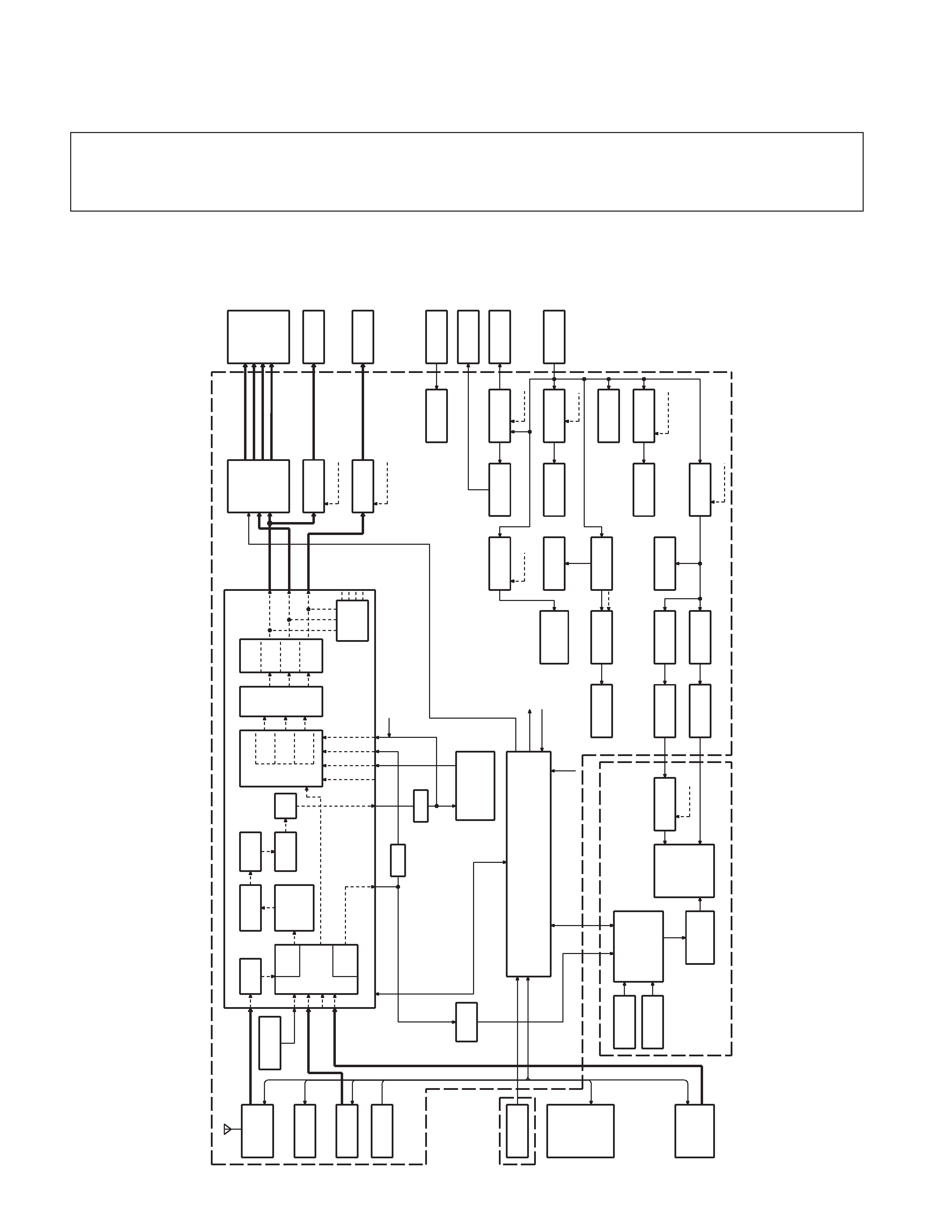
BLOCK
DIA
GRAM
This
ser
vice
man
ual
does
not
contain
inf
or
mation
on
the
f
ollo
wing:
mechanism
por
tion
f
or
MD
(BLOCK
DIA
GRAM,
COMPO-
NENTS
DESCRIPTION,
MICR
OCOMPUTER'S
TERMINAL
DESCRIPTION,
MECHANISM
OPERA
TION
DESCRIPTION,
AD-
JUSTMENT)
On
this
topic
,please
ref
er
to
the
dedicated
ser
vice
man
ual
f
o
rthe
MD
mechanism
X92-4570-00
(B51-7887-00).
KMD-6527
3
SUB-CIRCUIT UNIT (X16-2510-10)
Ref. No.
Application / Function
Operation / Condition / Compatibility
IC1
Panel
µcom
IC2
3.3V Regulater
The power supply of IC and VFD (Logic) which are driven by 3.3V
IC3
Remote Control IC
IC4
Buffer IC
It is change into 3.3V from 5V
Q1
FL BLK SW
VFD is turned on when Q1's base level goes "H"
Q2,3
FL+B SW
FL+B (VDD2) is turned on when Q2's base level goes "H"
Q4
SW5V
The power supply of IC3 is turned on when Q4's base level goes "L"
Q6
LED SW
LED is turned on when Q6's base level goes "H"
Q7,9
Red LED SW
RED LED is turned on when Q7's base level goes "L"
Q8,10
Green LED SW
GREEN LED is turned on when Q8's base level goes "L"
Q11,12
Blue LED SW
BLUE LED is turned on when Q11's base level goes "L"
SUB-CIRCUIT UNIT (X16-2520-00)
Ref. No.
Application / Function
Operation / Condition / Compatibility
PH1
MD Disk Det
When base voltage is set to "L", they are those with a disk.
ELECTRIC UNIT (X34-3012-72)
Ref. No.
Application / Function
Operation / Condition / Compatibility
IC1
System
µCOM
Controls FM/AM tuner, the changer, CD/MD mechanism, Panel, volume and tone.
IC2
E.Vol & N.C.MPX
Controls the source, volume, tone and FM multiplex detector
IC3
A8V Ref Power Supply
Output 1.27V
IC4
Power IC
Amplifies the front L/R and the rear L/R to 50W or 47W maximum.
IC7
SW Regulator
Power Supply for mp3
IC10
Muting logic IC
Controls logic for muting.
IC11
Reset IC
"L" when detection voltage goes below 3.6V or less.
IC12
RDS decoder
IC13
Panel mecha motor driver
Panel mecha control
IC14
Level meter Buffer
The signal of IC2 is sent to Panel
µcom
IC20
SW Regulator
Power Supply for VFD
Q1,2
B.U.5V AVR
While BU is applied, BU5V AVR outputs +5V.
Q3,4
SW5V
When Q4'base goes Hi, SW5V outputs +5V.
COMPONENTS DESCRIPTION
IN
Panel mecha
IN1
IN2
LL
WAIT
LH
OPEN
HL
CLOSE
HH
STOP
KMD-6527
4
Ref. No.
Application / Function
Operation / Condition / Compatibility
Q5
SW14V
When Q5'2pin goes Hi, SW14V outputs 14V.
Q6,8
AUDIO8V AVR
When Q6'2in goes Hi, A8V AVR outputs 8.0V.
Q7,9
SERVO+B AVR
When Q9'base goes Hi, S+B AVR outputs 7.5V.
Q10,11
SERVO+B AVR (Panel Mecha)
When Q10'base goes Hi, S+B AVR outputs 8.5V.
Q12
SW for IC7
When Q12'base gose Lo, IC7 is turned on.
Q13,15,16
FL&ILL AVR
When Q13'2pin goes Hi, ILL AVR outputs 10.5V.
Q27,30
P-CON SW
When Q30'base goes Hi, AVR outputs 14V.
Q28,29
P-CON Protection
Protect Q27 by turning on when P-CON output is grounded.
Q31
Ex Amp Control Buffer
Q32
Small lamp det SW
When Q32'base goes Hi, Q32 is turned on.
Q33,34
SERGE Det.
When Q33'base goes Hi, IC4 is changed into a standby state.
Q35
BU det
When Q35'base gose Hi, Q27 is turned on.
Q36
ACC det
When Q36'base gose Hi, Q29 is turned on.
Q37,38
Pre-out mute driver
When a base gose Lo, mute driver is turned on.
Q39
Sub-out mute driver
When a base gose Lo, mute driver is turned on.
Q40
AC-out mute driver
When a base gose Lo, mute driver is turned on.
Q41,42
AM+B SW
When Q42'base gose Hi, AM+B is out.
Q43
Composite signal buffer for RDS
DSI lights when the base is "L".
Q44
DSI Driver
DSI turns off when the base is "H".
DSI turns on and off when panel is taken off.
Q45,46
Panel 5V SW
When Q46'base gose Hi, PANEL 5V is out.
Q47~50
Pre-out mute SW
When a base gose Hi, Pre-out is muted.
Q55
Noise buffer
RDS Noise
Q56,57
AC-out mute SW
When a base gose Hi, AC-out is muted.
Q58,59
Sub-out mute SW
When a base gose Hi, Sub-out is muted.
Q60
Level meter mute SW
When a base gose Hi, Level meter is muted.
COMPONENTS DESCRIPTION
KMD-6527
5
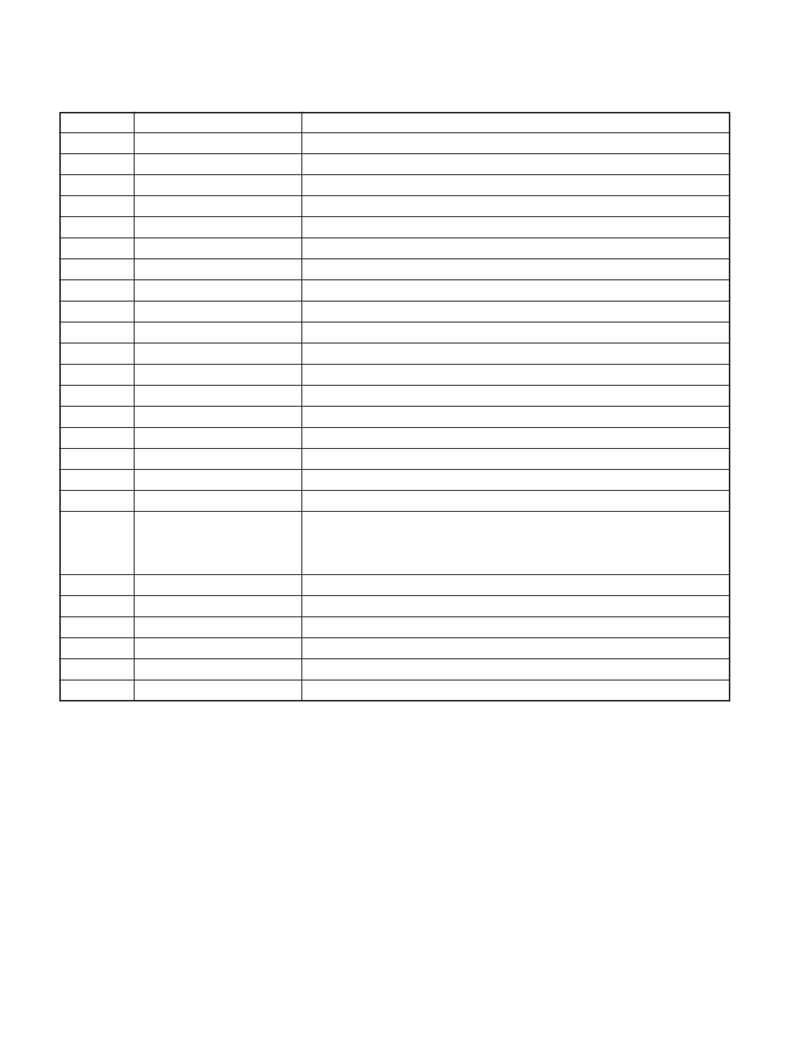
MICROCOMPUTER'S TERMINAL DESCRIPTION
SYSTEM MICROCOMPUTER : 30624MGPA27GP (X34 : IC1)
Pin No.
Pin Name
Module
I/O
Application
Truth Value
Processing Operation Description
Table
1~4
NC
O
Not used
Output : L
5
OPEL_REMO
EXTRA
I
External display remote control input
6
BYTE
-
0V GND direct connection
7
CNVSS
I
Used when writing to system
µcom
Pull down
8
XCIN
I
Sub clock input (32.768kHz)
9
XCOUT
I
Sub clock output (32.768kHz)
10
RESET
-
Reset terminal
L : Reset
11
XOUT
-
Main clock output (16.0MHz)
12
VSS
-
13
XIN
-
Main clock input (16.0MHz)
14
VCC1
-
15
NMI
I
Not used
16
ES_SW
EXTRA
O
System E's light usage switching
u
L : FLAT, H : E's Light
17
RDS_CLK
TUNER
I
RDS decoder CLK input terminal
18
LX_REQ_S
LX_M
I
Communication request from slave unit
19
PON_AM
TUNER
O
AM power supply control
AM operation : H, Non-AM operation : L
20
MUTE_LEVEL
EXTRA
O
LEVEL_METER MUTE terminal
Mute ON : H, Mute OFF : L
21
TUN_IFC_OUT
TUNER
I
F/E IFC OUT input terminal
H : Station detect, L : No detect
22
RDS_AFS_L
TUNER
I/O
Constant switching at noise detect
r
Refer to truth value table.
23
RDS_AFS_M
TUNER
I/O
Constant switching at noise detect
r
Refer to truth value table.
24
RDS_QUAL
TUNER
I
RDS decoder QUAL input terminal
25
RDS_DATA
TUNER
I
RDS decoder DATA input terminal
26
PWIC_BEEP
PWIC
O
Beep output
27
TUN_SCL
TUNER
I/O
F/E I2C clock output terminal
(MAX 400kHz)
28
TUN_SDA
TUNER
I/O
F/E I2C data input/output terminal
29
PAN_DATA
to PANEL I/O
Between-panel communication (Bi-directional)
30
PAN_CLK
to PANEL I/O
Between-panel communication clock
31
PAN_SCREQ
to PANEL I/O
Between-panel communication request
termnal (Used also for PN_DET)
32
PAN_PNREQ
to PANEL
I
Between-panel communication request terminal
33
AUD_SDA
AUDIO
I/O
E-VOL I2C data input/output terminal
MD_SDA
MD
I/O
MD mechanism I2C data input/output terminal
34
AUD_SCL
AUDIO
I/O
E-VOL I2C clock output terminal
MD_SCL
MD
I/O
MD mechanism I2C clock output terminal
35
PON_PAN
Power supply I/O
Panel 5V control terminal
ON : H, Momentary power down, Panel come
off and 11 minutes after ACC_OFF : Hi-Z
36
DSI
EXTRA
I/O
(D) SI control terminal
OFF : Hi-Z, Panel come off : Pulse driven,
ILL_ON and OPEN (Power_ON) : H