© 2003-11 CREATED IN JAPAN
B53-0110-00 (N) 0
MD CHANGER
KMD-300/GD2
SERVICE MANUAL
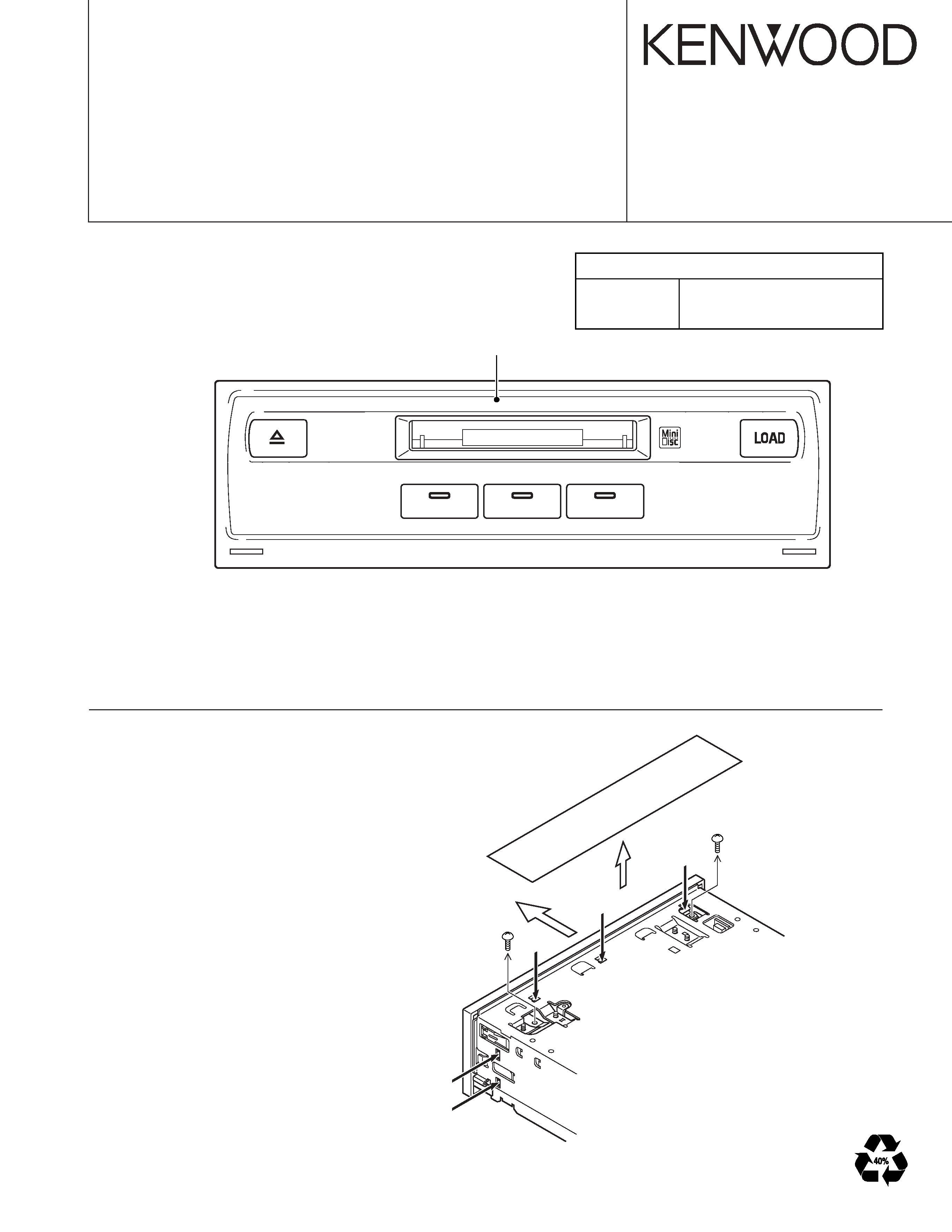
Audi md changer
Panel assy
(A64-2691-12)
Audi GENUINE
GENUINE PARTS No.
Hardware
4E0 035 121 41
Software
4E0 910 121 0001 300
BOTTOM
A
C
B
B
C
C
C
C
C
How to Take the Panel Assembly Off
1) Take the sheet (A) off.
2) Remove screw (B).
3) While pressing on the hook (C), take the panel
assembly off.
KMD-300/GD2
2
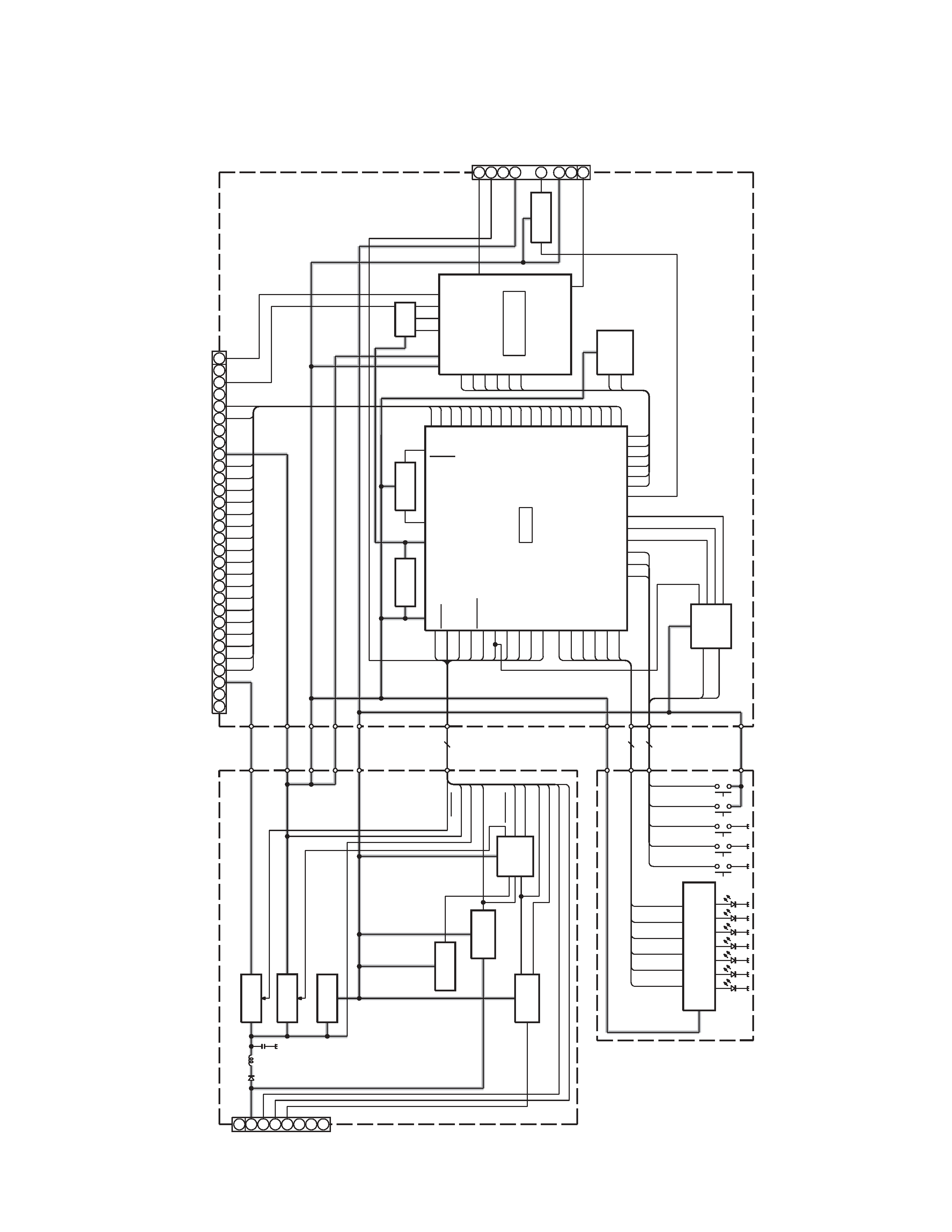
BLOCK
DIA
GRAM
G&H
6.5V
IC3
IC2
5V DIG.
5V CONT.
IC1
BU. DET.
IC30
SW to
IC31
Q41-43
DIAG
CIRCUIT
POW
POWER
ON
IC32-34
LOGIC
LED DRIVER
Q60-66
MECHA CONNECTOR
IC70
KEY
HOLD
IC1
3.3V
WDTIMER
IC90
EEPROM
IC91
IC30
H8S2626
u-COM
IC151
OS8104
MOST
TRANCEIVER
DIR
IC150
PIGTAIL
MOST
OPT ATT.
J1
CN100
J180
1
2
3
4
5
6
7
8
GND
BU+12V
ID-X
ID-Y
S +6.5V
M-BU+5V
D+5V
A+5V
BU+5V
DIAG
PON
LEV6V
SW to POW
STATUS
HOLD
DIAG IN
DIAG OUT
PINX
PINY
LED
EJECT
LED
DISC1
LED
DISC2
LED
DISC3
LED
GUIDE
LED
LO
AD
SW
DISC1
SW
DISC2
SW
DISC3
SW
EJECT
SW
LO
AD
30 29 28 27 26 25 24 23 22 21 20 19 18 17 16 15 14 13 12 11 10 9
8
7
6
5
4
3
2
1
SW EJECT
SW LOAD
SW
DISC1
SW
DISC2
SW
DISC3
SW
EJECT
SW
LO
AD
CLEAR
OPT
A
T
T
LEV16V
10
6
5
LED LOAD
LED GUIDE
LED DISC3
LED DISC2
LED DISC1
LED EJECT
HOLD
DIAGOUT
PINX
PINY
DIAGIN
STATUS
LEV16V
PON
SW to PWR
LEV6V
WDTN
RESET
D
ATA
I
N
8
7
6
5
4
3
2
1
RX
STATUS
GND
BU+5V
ATT
D+5V
GND
TX
ST
A
TUS
LRC
IN
C
IN
CL
LRCL
MCLK(22.5792MHz)
D.AUDIO(IEC60958)
D+5V
BU+5V
(X14-6912-70) (A/2)
(X14- ) (B/2)
(X25-9252-70)
KMD-300/GD2
3
DISPLAY UNIT (X14-6912-70)
Ref. No.
Application/Function
Operation /Condition/Compatibility
IC1
Stabilized power supply
Supplies Bu +5V to IC30, IC31, IC32, IC33, IC34, etc.
IC2
Stabilized power supply
Supplies D.+5V to X25 board
IC3
Stabilized power supply
Supplies +6.5V to mechanism X33
IC30
Reset IC
OUT=H when BU+5V is above 4.2V
IC31
1 pulse oscillation
Oscillates 1 pulse at rise of BU
IC32
NOT circuit
((~STATUS | | DIAG | | Sw to Pow) &&-LEV6) | | HOLD=H, then D.+5V ON
IC33
OR circuit
((~STATUS | | DIAG | | Sw to Pow) &&-LEV6) | | HOLD=H, then D.+5V ON
IC34
D flip-flop
Detects downward slope of J1 DIAG
Q1
Switch
Q1 base =L, then LEV16=12V
Q2
NOT circuit
Q2 base =H, then Q1 base =L
Q40
NOT circuit
J1 DIAG=L, then IC33 A3 input=H
Q41
NOT circuit
CN1 DIAGOUT=H, then J1 DIAG=L
Q42
Excess current protection
Limit Q41 emitter current
Q43
NOT circuit
J1 DIAG=L, then CN1 DIAGIN=H
Q60
Switch
CN2 LED1=H, then D60 lights up.
Q61
Switch
CN2 LED2=H, then D61 lights up.
Q62
Switch
CN2 LED3=H, then D62 lights up.
Q63
Switch
CN2 LED4=H, then D63 lights up.
Q64
Switch
CN2 LED5=H, then D64 lights up.
Q65
Switch
CN2 LED6=H, then D65 lights up.
Q66
Switch
CN2 LED6=H, then D66 lights up.
ELECTRIC UNIT (X25-9252-70)
Ref. No.
Application/Function
Operation /Condition/Compatibility
IC1
Stabilized power supply
Supplies 3.3V to IC30 and IC150.
IC30
µ-com
Controls various sections of the set.
IC70
D flip-flop
Detects rise of key input for LOAD/EJECT
IC71
NAND circuit
IC70 CLR=~ (IC90 RESET&&IC30 CLEAR)
IC90
RESET IC
D+5V is above 4.2V, then RESET=H.
IC91
EEPROM
Saves backup data.
IC150
DIR
Converts IEC60958 (SPDIF) signal to 3-line serial.
IC151
MOST transceiver
Signal processing IC for optical input/output
Q30
Switch
PF3=L, then AVREF ON.
Q70
NOT circuit
CN70 EJECT=H, then IC30 EJECT=L
Q71
NOT circuit
CN70 LOAD=H, then IC30 LOAD=L
Q180
NOT circuit
MOST ATT=H, then Q181 base=L
Q181
Switch
MOST ATT=H, then increase optical output.
COMPONENTS DESCRIPTION

KMD-300/GD2
4
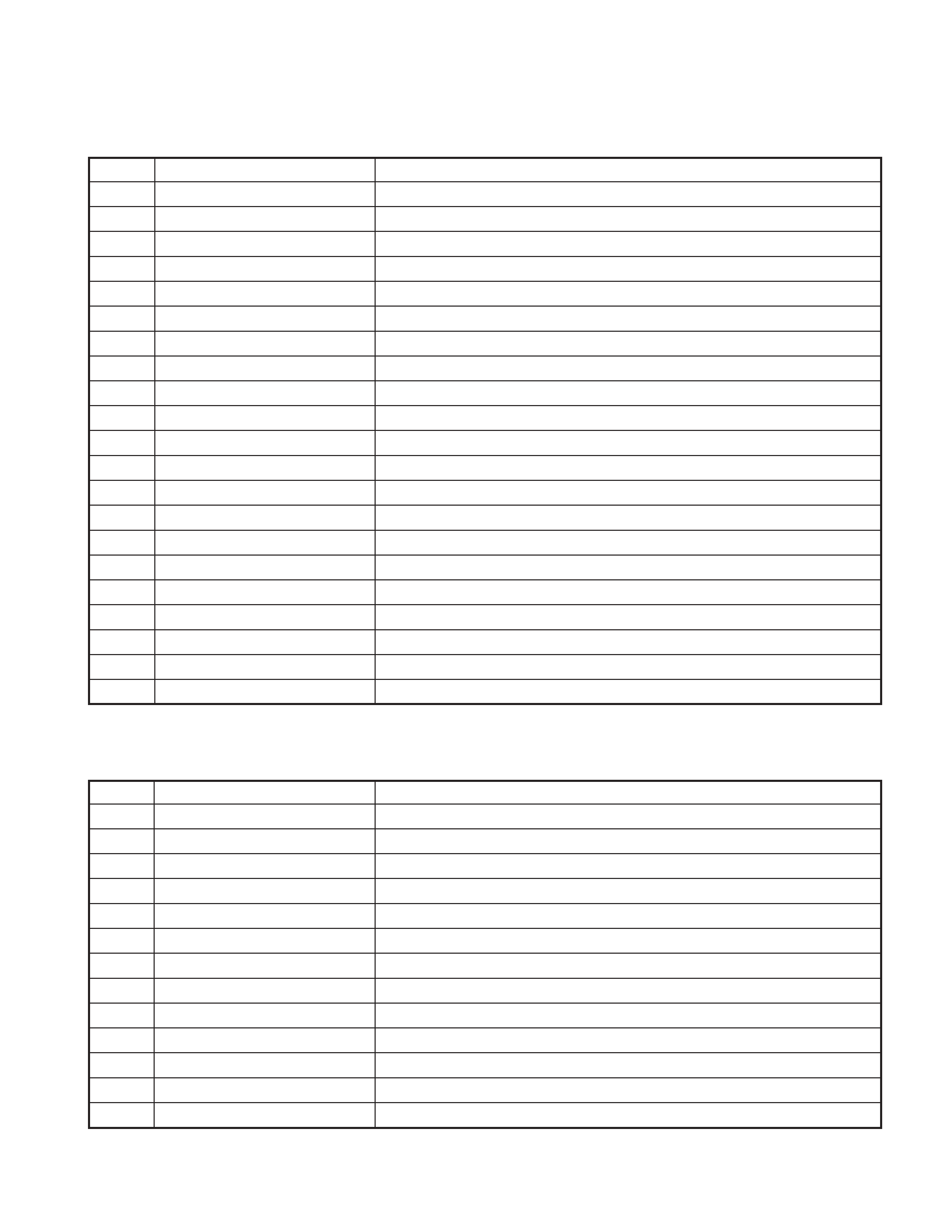
MICROCOMPUTER'S TERMINAL DESCRIPTION
MICROCOMPUTER : HD64F2626FA20I (X25 : IC30)
Pin No.
Pin Name
I/O
Application
1ATT
O
MOST TX attenuate
2
MOST_INT
I
MOST data reception interrupt
3
BEEP
O
BEEP output
4
ERROR
I
MOST error signal
5
DIR_CS
O
DIR CS
6
VCC1
7
HTxD
8
VSS1
9
HRxD
10
MMUTE
I
Mechanism mute detection
11
SS1_SW
I
Stock1 Detection of disk/No disk SW
12
SS2_SW
I
Stock2 Detection of disk/No disk SW
13
SS3_SW
I
Stock3 Detection of disk/No disk SW
14
MS_SW
I
EJECT complete detection SW
15
VSS2
16
FS_SW
I
LOAD start detection SW
17
PVCC1
18
OS_SW
I
Wrong direction detection SW
19
NC
20
MSTOP
O
Mechanism control Wake Up
21
MRST
O
Mechanism control RESET
22
M0
O
M1, M2, M3 control output
23
M1
O
LO/EJ control output
24
M2
O
Mechanism roller attach control output
25
M3
O
Mechanism rising order control output
26
NC
27
NC
28
MSDA
I/O
Mechanism I2C data
29
MSCL
I/O
Mechanism I2C clock
30
DIR_ERR
I
DIR error
31
DIR_TX
O
DIR control output
32
DIR_RX
I
DIR control input
33
DIR_CLK
O
DIR clock
34
SDA
I/O
MOST I2C data
35
SCL
I/O
MOST I2C clock
36
LED1
O
MD1 eject SW LED
37
VSS3
38
LED2
O
MD2 eject SW LED
39
PVCC2
40
LED3
O
MD3 eject SW LED
41
LED4
O
Load SW LED
42
LED5
O
Eject SW LED
43
LED6
O
Insert slot LED
44
CLEAR
O
Hard key buffer clear
45
MOST_WRITE
46
NC
47
TXD
O
Flash writer data output
48
RXD
I
Flash writer data input
49
NC
50
OSC1

KMD-300/GD2
5
Pin No.
Pin Name
I/O
Application
51
OSC2
52
PVCC3
53
MD0
54
VSS4
55
MD1
I
µ-com mode switching
56
MD2
I
µ-com mode switching
57
PLLVSS
58
PLLCAP
59
PLLVCC
60
RES
I
µ-com resetting
61
NMI
62
STBY
63
VCC2
64
XTAL
65
VSS5
66
EXTAL
67
FEW
I
Flash write enable
68
NC
69
PON
O
Peripheral circuit power supply control
70
SA_SW
O
SA switch
71
HOLD_SW
O
SD switch
72
LPSCO
O
Vref control
73
WDT_OFF
O
Watch dog timer count output
74
DIAG_OUT
O
DIAG output
75
DIAG_IN
I
DIAG input
76
AVCC
77
Vref
I
Reference voltage input
78
MLPS
I
Mechanism location position detection
79
PS_SW
I
Play position detection of disk/No disk SW
80
LS_SW
I
Load complete SW
81
CS_SW
I
roller attach/detach SW
82
BU_DET
I
Power supply +B input
83
LEV16
I
Power supply voltage detection
84
NC
85
LEV_6
I
Power supply voltage <6V
86
DISK1
I
MD1 select SW
87
DISK2
I
MD2 select SW
88
DISK3
I
MD3 select SW
89
LOAD
I
LOAD SW
90
EJECT
I
Eject SW
91
SW_TO_PW
I
Power supply control
92
ID-X
I
Unit position detection
93
ID-Y
I
Unit position detection
94
AVSS
95
VSS6
96
WDTOVFA
97
PVCC4
98
NC
99
STATUS
MOST status
100
MOST_RST
MOST reset
MICROCOMPUTER'S TERMINAL DESCRIPTION