This service manual does not include information on the CD mechanism assembly (exploded view, parts list,
schematic diagram or mechanism operation description).
For such information, please refer to the CD mechanism assembly service manual (X92-4460-0x : B51-7891-00).
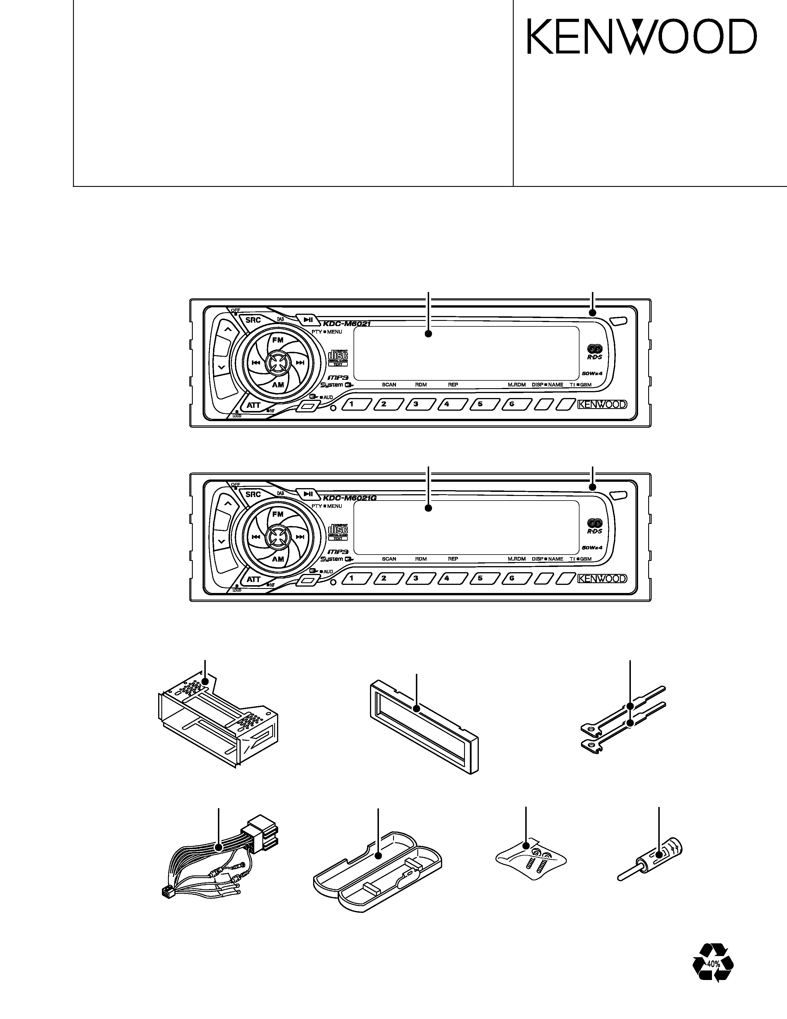
Antenna adaptor
(T90-0523/0534-05)
Screw set
(N99-1656-05)
Lever
(D10-4589-04)x2
Mounting hardware assy
(J21-9716-03)
Escutcheon
(B07-3055-02): KDC-M6021
(B07-3054-02): KDC-M6021G
Plastic cabinet assy
(A02-1486-13)
DC cord
(E30-4958-05)
Front glass
(B10-4195-01)
Panel assy
(A64-2606-02)
KDC-M6021G
Front glass
(B10-4179-01)
Panel assy
(A64-2601-02)
KDC-M6021
© 2002-1 PRINTED IN JAPAN
B51-7894-00 (S) 1928
CD RECEIVER
q
SERVICE MANUAL
KDC-M6021/G
KDC-M6021/G
2
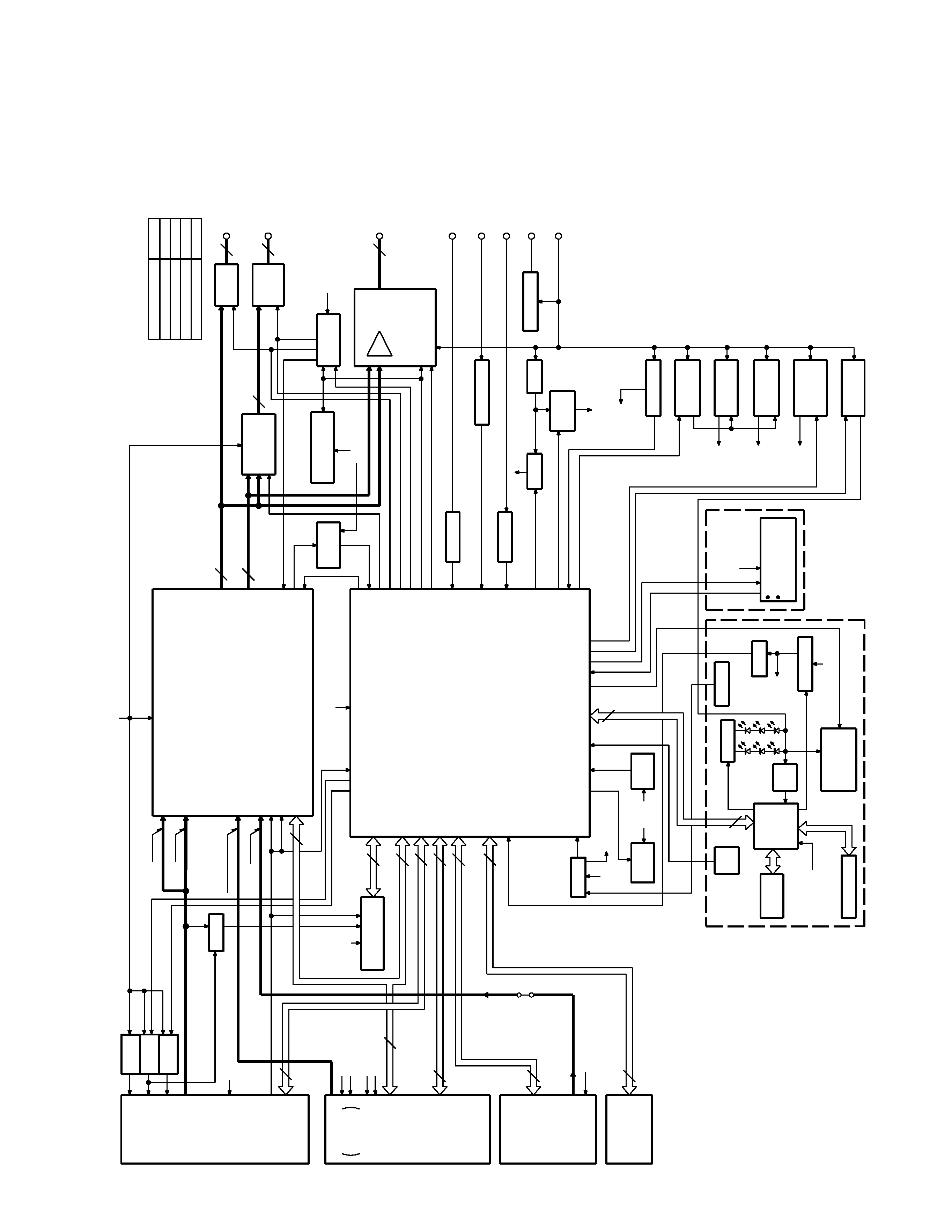
BLOCK
DIAGRAM
CH
CD MECHA
F/E
FM+B
PLL+B
AM+B
BUFF
E-VOL
SYSTEM
MI-COM
DECODER
RDS
MP3
NORMAL
WIRED
OEM DISP
RST IC
DET
FLIP
LCD (NEGA)
MATRIX
KEY
G/R SW
RST SW
REMO ON
BACKLIGHT
LCD
W-ILL
DRIVER
LCD
REMO
GUIDE
ILL
SW
OPEN
OUT
REMO/
BU5V
SW5V
SERVO
+B
PANEL
2WAY MUTE
ACC DET
DIMMER
TEL-MUTE
ACC
DIMMER
POWER IC
SP OUT
MUTE
PRE OUT (FRONT)
MUTE
PRE OUT (NF/REAR)
MUTE
DRIVER
OP AMP
SWITCHED
PROTECTION
THERMAL
NOISE
BUFFER
5V
BU DET
SW14V
A8V
CD
MACHA+B
ILLUMI
+B
(for MP3)
EJECT ILL/DSI
(SW AND LED)
EJECT KEY
X89-252
BACK UP
P-CON
P-CON
Q45,47
Q46,48
IC7
IC1
& N.C. MPX
IC2
Q52
IC8
Q54
S1
AVR
LCD
ED1
Q7
Q3,4
IC2
Q6
IC1
Q5
Q16,17
Q18
Q14,15
IC11,Q51
Q19-22
Q33
Q34
Q26
Q13
Q11,12
Q55
Q27,29,30,32
IC6
Q43
Q7,8
IC4
Q5,6
Q1,2
IC3,
ANT-CON
DATA C
CH-CON
DATA H
REQ H
RST
CLK
REQ C
CD MECHA+B
SERVO+B
PLL DATA
PLL CLK
M STOP
M RST
SW4
MUTE R
MUTE L
LO/EJ
MOSW
SW2
SW3
SW1
S-METER
IFC OUT
SW5V
3
P
ANEL
DET
GUIDE
ILL
MP IN
AFS
LEVEL
RDDA
FM
AM
A 8V
(for MP3)
BU5V
A8V
3
2
2
3
10
7
3
SW5V
10
SDA
SCL
AUDIO OUT
7
BACK UP
3
2
O-CLK
O-DATA
O-CE
REMO
RESET
BU5V
MUTE
DRIVER
PANEL5V
PANEL5V
5
CD
AM+B
FM+B
S-METER
RDCK
RQUAL
BU5V
5
BU5V
FLIP
DET
L
D
ATA
S
L
CE
L
CLK
L
D
ATA
L
L-INH
DIMMER-CON
EJECT
EJECT
ILLUMI/DSI
ILL
ON
CD
MECHA+B
SW5V
(E) TYPE
CD (MP3,NORMAL)
3600mV
CHANGER
FM
AM
1372mV
855mV
3600mV
2
2
BU5V
8
2
2
2
QUAL
S MUTE
REAR L/R
FRONT L/R
AFS
NOISE
N/F SW
PRE MUTE
N/F MUTE
P MUTE
MUTE
BEEP
BU5V
MUTE
DRIVER
P-ON
PANEL5V
SW5V
CH-AUX
MODE
PRE OUT OUTPUT VOLTAGE
DIMMER
PHONE
ACC DET
BU DET
251mV
230mV
1200mV
(MP3,NORMAL)
1200mV
KDC-M6021/G
3
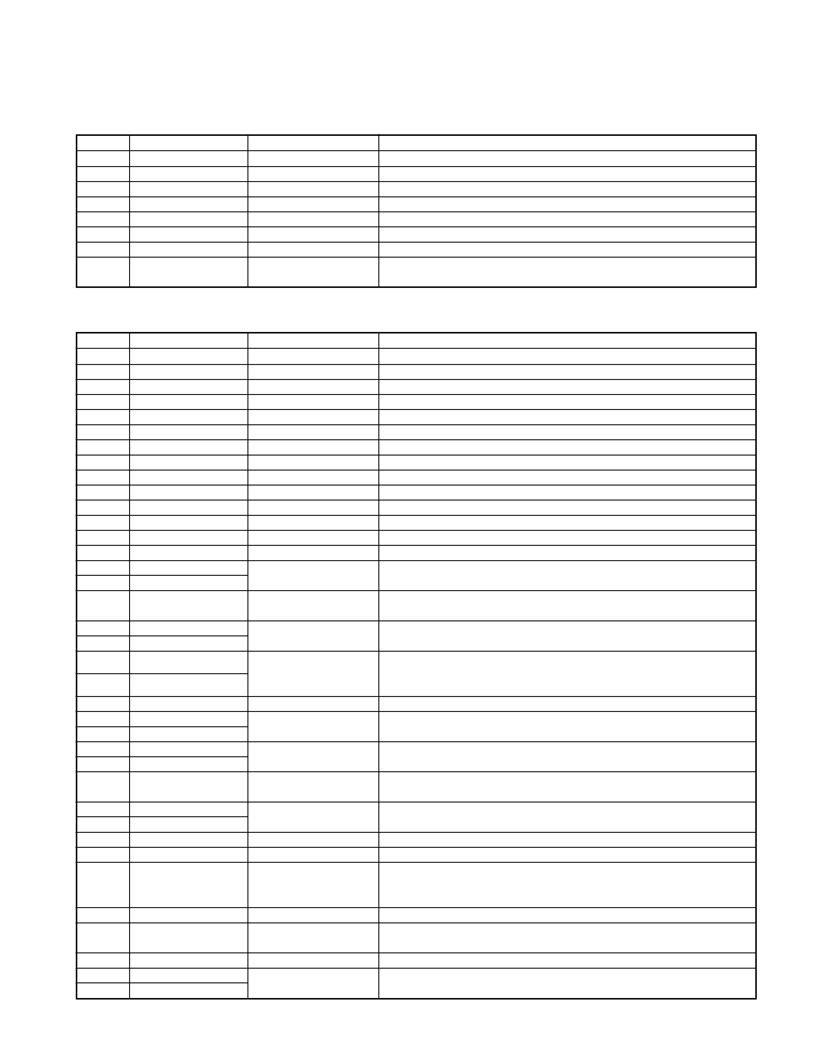
COMPONENT DESCRIPTION
q SWITCH UNIT (X16-1662-70)
Ref.No.
Component Name
Application/Function
Operation/Condition/Compatibility
IC1
LC75808W
LCD driver with key matrix
IC2
RS-171
Remote control sensor IC
Q1
DTA114EUA
Key permission SW
For the key scanning start and the key detection SW
Q3
2SD2114K
Key illumination red SW
When a base goes Hi, RED LEDs are turned on.
Q4
2SD2114K
Key illumination green SW
When a base goes Hi, GREEN LEDs are turned on.
Q5
2SC4081
VLCD AVR
For LCD driver IC
Q6
DTA114EUA
REMO SW
While a base goes Lo, PAN 5V is supplied to the remote control sensor IC.
Q7
2SC4081
Dimmer SW
Usually Q7's base goes Hi. When DIMMER mode is selected, pulse
wave shape is applied to Q7's base.
q ELECTRIC UNIT (X25-9202-71)
Ref.No.
Component Name
Application/Function
Operation/Condition/Compatibility
IC1
UPD703030GFA03
System MI-COM.
IC2
TDA7407D
E.VOL & N.C.MPX IC
IC3
TC74HC02AF
Mute logic
2-input NOR x 4
IC4
TA8273H
Power IC
IC6
NJM2123V-TE2
Switched Op. Amp.
IC7
SAA6581T
RDS decoder
IC8
S-80837ANNP
Reset IC
When BU 5V voltage is less than 3.7V, IC outputs Lo.
IC11
SI-8050JD
CD+5V AVR
DC/DC converter
Q1
DTC143TUA
Audio mute SW
When a base goes Hi, Front R Ch. pre-out is muted.
Q2
DTC143TUA
Audio mute SW
When a base goes Hi, Front L Ch. pre-out is muted.
Q5
2SD2114K
Audio mute SW
When a base goes Hi, NON-F R Ch. pre-out is muted.
Q6
2SD2114K
Audio mute SW
When a base goes Hi, NON-F L Ch. pre-out is muted.
Q7
DTA124EUA
Mute driver for pre-out mute SW
When a base goes Lo, Q7 is turned on for driving NON-F mute SW.
Q8
DTA124EUA
Mute driver for pre-out mute SW
When a base goes Lo, Q8 is turned on for driving Front mute SW.
Q11
2SC4081
BU 5V AVR
While BACKUP is applied, BU 5V AVR outputs +5V.
Q12
2SA2057
Q11 and Q12 are inverted Darlington connection.
Q13
2SA1576A
SW 5V
While a base goes Lo, SW 5V is supplied to the microprocessor
peripheral circuits.
Q14
2SC4081
A.+8V AVR
When Q14's base goes Hi, Q15 is turned on, and A.+8V AVR outputs +8.3V.
Q15
2SA2057
Q14 and Q15 are inverted Darlington connection.
Q16
DTC124EUA
A.+8V AVR and SERVO +B AVR ON/OFF control
Q17
DTA124EUA
SW14V
While Q16's base goes Hi, Q17 is turned on, and A.+8V AVR and
SERVO +B AVR are working.
Q18
2SD2375
SERVO +B AVR
When Q18's base goes Hi, SERVO +B AVR outputs +7.6V.
Q19
DTC124EUA
ILL +B AVR SW
ILL +B AVR ON/OFF control
Q20
DTA124EUA
While Q19's base goes Hi, Q20 is turned on, and ILL +B AVR is working.
Q21
2SB1184
ILL +B AVR
While Q22's base goes Hi, Q21 is turned on, and AVR outputs +10.7V.
Q22
2SC4081
Q21 and Q22 are inverted Darlington connection.
Q26
DTC144EUA
Small lamp detection SW
When vehicle small lamps turn on, Q26's base goes Hi, and Q26 is
turned on .
Q27
DTC114YUA
P-CON SW
When Q27's base goes Hi, Q32 is turned on.
Q32
2SB1277(Q,R) or 2SB1434
Works during POWER ON mode.
Q29
DTA124EUA
P-CON. protection inhibit SW
Prevents Q30 tuning ON during start-up after power ON.
Q30
2SA1576A
P-CON. protection SW
Protect Q32 by turning ON when P-CON output is grounded.
While BACKUP is applied, a base goes Hi, and Q33 is turned on.
Q33
2SC4081
BU detection SW
When momentary power down has detected, a base goes Lo, and
Q33 is turned off.
Q34
2SC4081
ACC detection SW
While ACC is applied, a base goes Hi, and Q34 is turned on.
Q42
DTC124EUA
E. VOL. mute SW
When BU detection SW or MI-COM.'s mute is working, a base goes
Hi, and Q42 is turned on.
Q43
DTC143TUA
Noise buffer
Q45
DTC124EUA
FM+B SW
When Q45's base goes Hi, Q47 is turned on, and A.+8V is supplied to
Q47
2SB1277(Q,R) or 2SB1434
the F/E. Works during FM reception mode or RDS reception mode.

KDC-M6021/G
4
Q46
DTC124EUA
AM+B SW
When Q46's base goes Hi, Q48 is turned on, and A.+8V is supplied to
Q48
2SB1277(Q,R) or 2SB1434
the F/E. Works during AM reception mode.
Q51
2SC4081
CD+5V AVR SW
When a base goes Hi, CD+5V AVR is working.
Q52
DTC143TUA
Composite signal buffer
Q53
DTA114YUA
EJECT illumination/DSI SW
When a base goes Lo, Q53 is turned on.
Q54
DTA114YUA
Guide illumination SW
When a base goes Lo, Q54 is turned on.
Q55
2SA1576A
Panel 5V SW
When a base goes Lo, Q55 is turned on.
Ref.No.
Component Name
Application/Function
Operation/Condition/Compatibility
COMPONENT DESCRIPTION
KDC-M6021/G
5
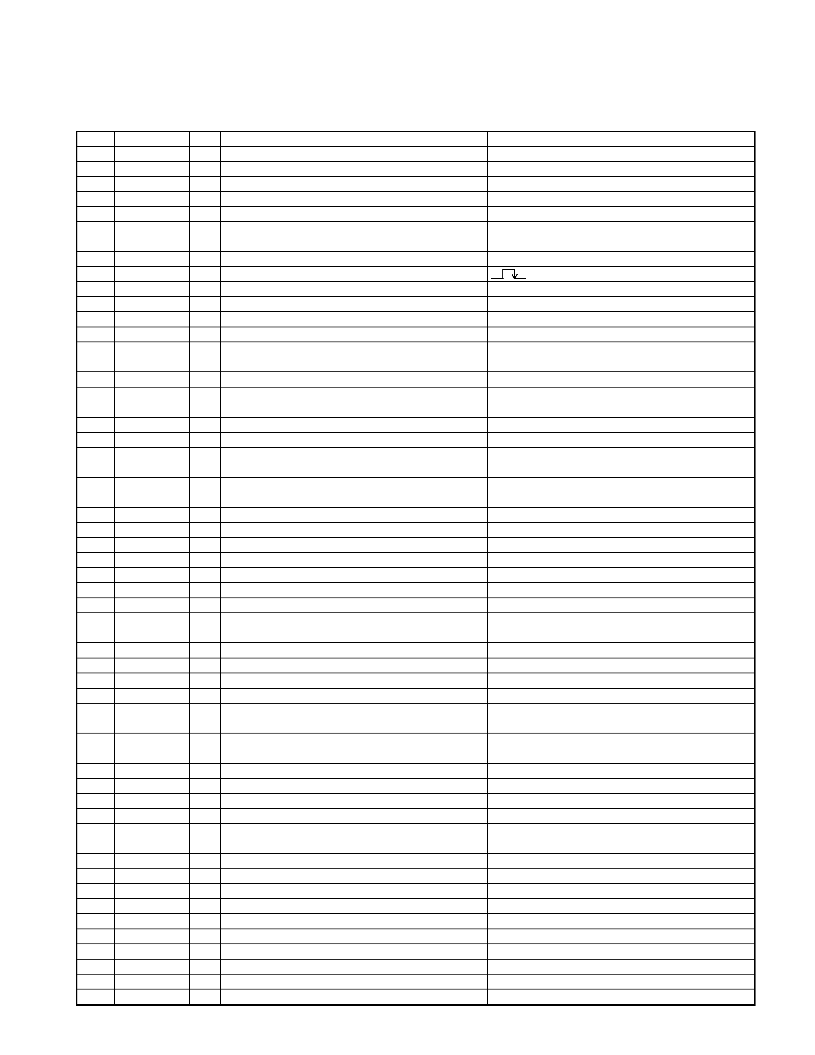
q IC1 (ELECTRIC UNIT : X25-9202-71)
Pin No.
Pin Name
I/O
Description
Processing Operation
1
L-DATAS
O
Data line to LCD driver
2
L-CLK
O
Clock output to LCD driver
3
PLL-DATA
I/O Data input/output terminal with F/E
4
PLL-CLK
I/O Clock output to F/E
5
AM+B
I/O AM+B control
Hi: During AM reception
6
FM+B
I/O FM+B control
Hi: During FM reception, Hi: During FM reception
if with RDS, RDBS
7
CH-CON
O
Changer control output
Lo: Standby mode, Hi: Operation mode
8
CH-RST
O
Reset output to changers
: Reset
9
EVDD
-
Positive power supply connection terminal
Connected to BU 5V lines.
10
EVSS
-
Ground connection terminal
Connected to GND lines.
11
AFS
O
Noise detection time constant switching terminal
Hi: During FM reception, Lo: During FM seek or AF search
12
BEEP
O
BEEP sound output
13
REMO
I
Data input from the remote control light sensor or
wired remote control
14
AUX SW
I/O CH/AUX inputs selector terminal
Not used(N.C.)
15
N/F SW
O
N/F selector terminal
Hi: Rear/N-F pre-outs are selected to Front output.
Lo: Rear/N-F pre-outs are selected to Rear output.
16
IC2-SDA
I/O Data line with IC2,CD mechanism MI-COM.
17
IC2-SCL
I/O Clock line with IC2,CD mechanism MI-COM.
18
PRE-MUTE
I/O Pre-out mute control terminal
Lo: When momentary power down detected, when
M-MUTE input is Lo.
19
N/F-MUTE
O
N-F pre-out mute control terminal
Lo: When momentary power down detected, N-F pre-
outputs selecting or OFF, when M-MUTE inputs is Lo.
20
DIMMER-CON
O
Dimmer control output
Hi: Dimmer OFF, Pulse wave shape: Dimmer ON
21
TEST
-
Test terminal
Not used(Connected to GND lines)
22
SVR
O
Power IC SVR control output
Not used(N.C.)
23
P-MUTE
O
Power IC mute output
Lo: ALL OFF mode, POWER OFF mode, TEL MUTE on
24
P-STBY
O
Power IC STBY control output
Hi: Power IC on, ALL OFF mode, Lo: Power IC off
25
MUTE
O
Mute control output
Lo: Mute off, Open: Mute on
26
SW5V
I/O SW5V control terminal
Lo: SW5V on, Hi-Z: SW5V off
27
BU DET
I
Momentary power down detection input
Hi : When momentary power down detected or BU OFF
Lo : BU ON
28
ACC DET
I
ACC detection terminal
Hi: ACC OFF, Lo: ACC ON
29
N.C
O
Not used(N.C.)
30
DIMMER
I
Small lights detection input
Lo: During vehicle small lamps turn on.
31
N.C
O
Not used(N.C.)
32
P-CON
I/O Power control output
Hi-Z: POWER OFF mode, ALL OFF mode, Hi:
POWER ON mode
33
ANT-CON
O
Antenna control output
Hi: During TUNER mode, TI reception mode, last
FM mode
34
RESET
I
Reset input terminal
Lo: System reset
35
XT1
I
Sub clock resonator connection terminal
Clock count during POWER OFF mode
36
XT2
-
Sub clock resonator connection terminal
37
REGC
-
Capacitor conection terminal for regulator inside microprocessor
38
X2
-
Main clock resonator connection terminal
Oscillation: POWER ON mode, Oscillation stop:
POWER OFF mode or momentary power down detected
39
X1
I
Main clock resonator connection terminal
40
VSS
-
Ground connection terminal
Connected to GND lines.
41
VDD
-
Positive power supply connection terminal
Connected to BU 5V lines.
42
CLKOUT
O
Internal system clock output
Not used(N.C.)
43
CD MECH +B
I/O MP3 CD mechanism power supply control output Lo: Power supply on, Hi-Z: Power supply off
44
P-ON
I/O SW14V control terminal
Lo: POWER OFF mode, Hi: POWER ON mode
45
O-DATA
I/O Data line with the external display device
Lo: The model without the external display device
46
O-CLK
I/O Clock line with the external display device
Lo: The model without the external display device
47
O-CE
I/O CE line with the external display device
Lo: The model without the external display device
48
N.C
O
Not used(N.C.)
MICROCOMPUTER'S TERMINAL DESCRIPTION