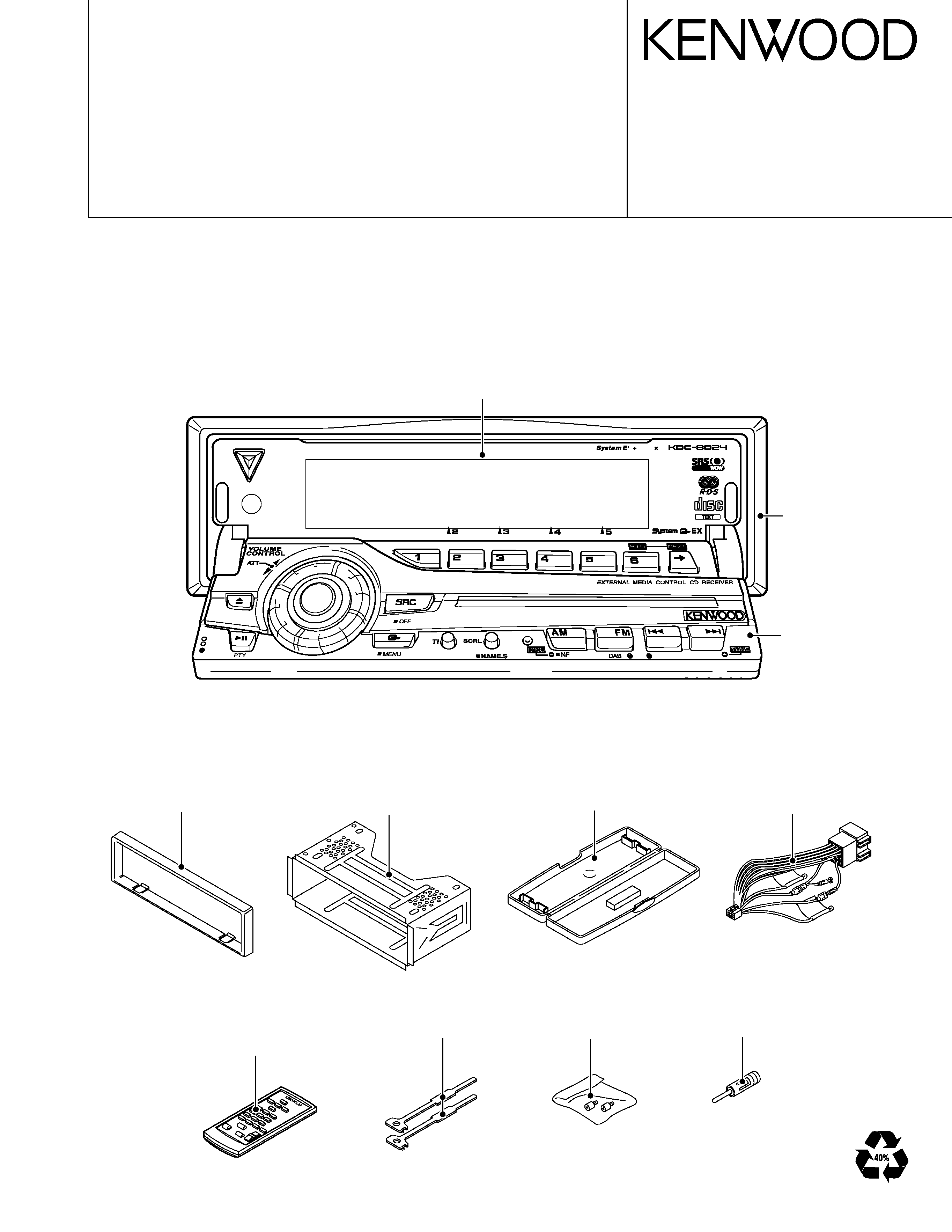
CD mechanism extension cord : W05-0935-00
Mounting hardware assy
(J21-9823-03)
DC cord (ISO)
(E30-4942-05)
Lever
(D10-4674-04) x 2
Plastic cabinet assy
(A02-2731-03)
Remote controller assy
(RC-420)
(A70-2026-05)
Screw set
(N99-1734-05)
Antenna adaptor
(T90-0552-05)
Escutcheon
(B07-3078-01)
50
4
W
DIGITAL AUDIO
COMPACT
s
Panel assy
(A64-2985-01)
Escutcheon
(B07-3078-01)
Panel assy
(A64-3002-02)
CD mechanism operation description is not in this service
manual.
Please, refer to service manual X92-4030-0x (B51-7867-00).
© 2003-2 PRINTED IN JAPAN
B53-0033-00 (N) 1874
CD RECEIVER
KDC-8024
SERVICE MANUAL
3
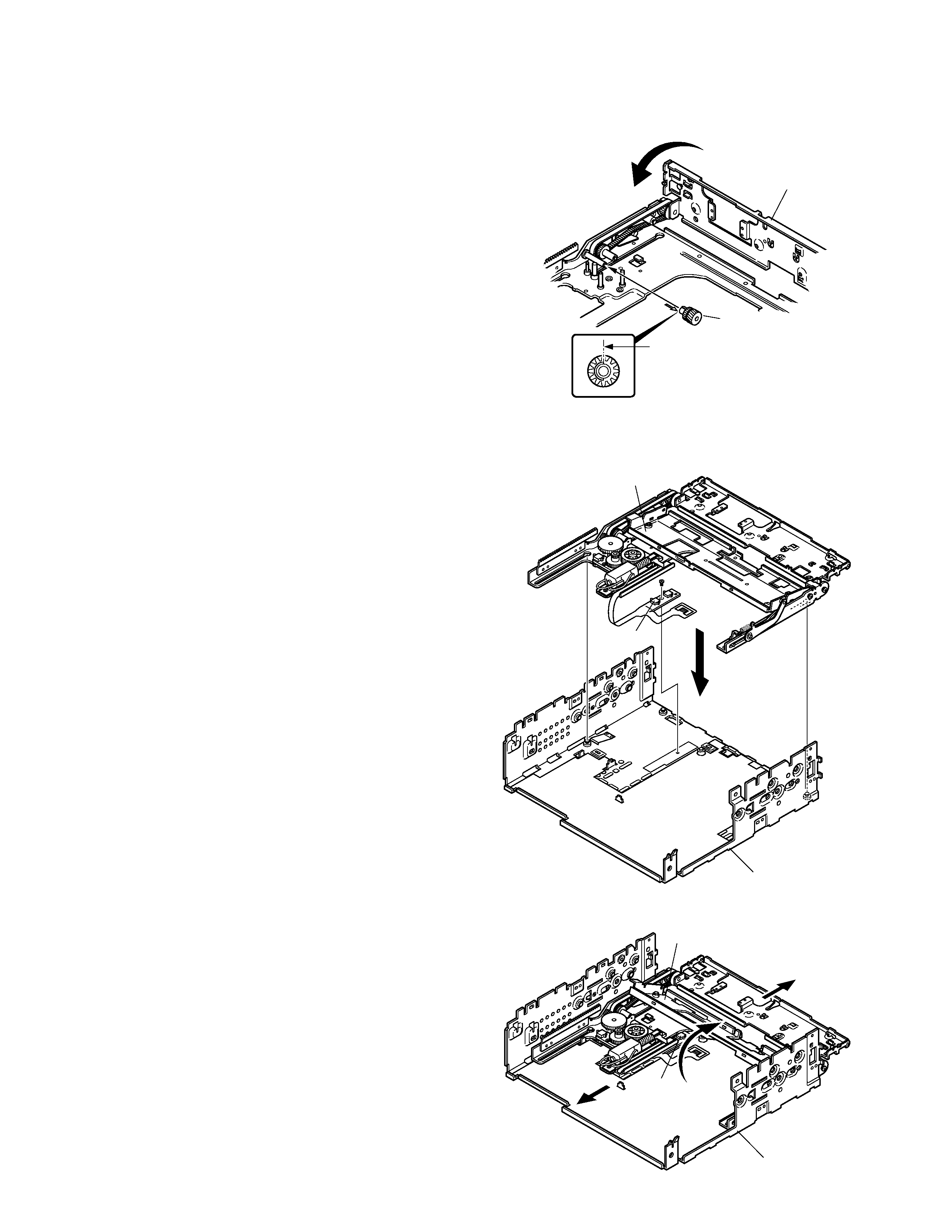
HOW TO THE PANEL MECHANISM ASSEMBLY
1. Fixed the position of operation side
(Fixed the horizontal position when the panel opened)
q The mounting hardware (281) of operation side is rota-
tion (A) into the stop position with close side.
w As figure (B) line is just above and the gear (230) at-
tached to pin.
B
A
Rotary to the
stop position
281
230
This line attached just above
Fig. B
(This figure from look at B arrow)
C
284
702
SW
D
E
F
702
SW
284
2. The slider assembly insert to bottom chassis
q The bracket for display panel (284) is leave down, in-
sert to the chassis (702). (C)
w The slider assembly insert to the chassis (702) after
that shift (D) direction.
e The bracket for display panel (284) is raised (E) direc-
tion.
r Keep the raising conditions, the slider assembly is shift
(F) direction.
(Note) Do not bend the knob of chassis detection switch
when the slider assembly insert.
KDC-8024
KDC-8024
3
BLOCK DIAGRAM
BUFFER
RDS
DECODER
BUFFER
REMO
RESET SW
KEY MATRIX
FL
u-COM
MPX
E-VOL
&
ACC DET
TEL MUTE
B.U DET
SYSTEM
DRIVER
MUTE
POWER
IC
ACC
TEL MUTE
BACK UP
SP OUT (FL)
RESET
KEY ILL
IC14
IC2
IC1
IC4
IC8
IC9
Q303,304
AM+B
AGC
E'S+
PRE MUTE
PRE MUTE
PRE MUTE
PRE OUT
(FRONT)
PRE OUT
(REAR)
(NF)
PRE OUT
OP AMP
OP AMP
OP AMP
SP OUT (FR)
SP OUT (RL)
SP OUT (RR)
EXT AMP
DIMMER
DIMMER
EXT.AMP.CON
ANT-CON
ANT CON
P-CON
P CON
WIRED REMO/
OPEL DISP I/F
FOCUS
SW
WOW
IC5
IC20
IC6
IC9
IC13
IC12
IC11
Q207,208
Q205,206
Q203,204
BU5V
SW 5V
SW 14V
5V
SERVO
FL+B
SW REG
A8V
PANEL
Q1,2
Q3,601
Q502,503
Q4,5
Q6-8
Q9,602
BU5V
SW5V
PANEL5V
SW14V
DC/DC
A8V
SERVO
CD4.7V
IC16
MOTOR
DR
DR
MOTOR
IC15
DC/DC
ROTARY
ENCODER
u-COM
IC11
SHIFT
LEVEL
BPF
PANEL
SW5V
FL+B
Q4
FL3.3V
Q2,3
EEPROM
EEP5V
Q501
IC1
Q23,24
Q26
Q25
IC18
Q27
Q29
IC10
Q6,10
Q11-14
IC19
S-METER
AUDIO OUT
SERVO
8V
BU5V
CD4.7V
BACK UP
FM
AM
CD
QUAL
CH
PANEL5
KEY
BU5V
8V
SW5V
8V
8V
SW5V
BPF
8V
8V
9V
9V
9V
8V
9V
SW5V
FL+B
FAC
AGC
8V
8V
BU5V
BU5V
BU5V
SERVO
TUNER
CD
CH
UNIT
MECHA
PANEL
TDF UNIT
SWITCH UNIT
DISPLAY
(X16-208)
(X16-212)
(X16-217)
(X25-964)
KDC-8024
4
q SUB-CIRCUIT UNIT (X16-2080-10)
Ref. No.
Application/Function
Operation/Condition/Compatibility
IC1
E2PROM
For security
q SUB-CIRCUIT UNIT (X16-2120-10)
Ref. No.
Application/Function
Operation/Condition/Compatibility
IC1
3.3V regulator
The power supply of IC and VFD (Logic) which are driven by 3.3V
IC2
Buffer IC
It is change into 3.3V from 5V
IC3
Remote control IC
IC4
Spectrum analyzer IC
IC5
Panel
µ-com
Q1, 2
FL+B SW
FL+B (VDD2) is turned on when Q2's base level goes "H"
Q3
REMO ON SW
The power supply of IC2 and IC3 is turned on when Q3's base level goes "L"
Q4
FL BLK SW
VFD is turned on when Q4's base level goes "H"
Q5
Blue LED SW
Blue LED is turned on when Q5's base level goes "H"
q SWITCH UNIT (X16-2170-10)
Ref. No.
Application/Function
Operation/Condition/Compatibility
Q1
DSI (Disabled System Indicator)
DSI blinks when the base goes "H/L"
Q2
KEY illumination SW (GREEN)
ON (KEY illumination green) when the base goes "H"
Q3
KEY illumination SW (RED)
ON (KEY illumination red) when the base goes "H"
q ELECTRIC UNIT (X25-9642-72)
Ref. No.
Application/Function
Operation/Condition/Compatibility
IC1
System
µ-com
IC2
E-vol & N.C. & MPX
IC3
Regulator IC for A8V
IC4
Power IC
IC5
System E's IC
IC6
Audio IC (WOW)
IC8
Reset IC
IC9
Logic IC for muting
IC10
Buffer for S.A
IC14
RDS dcoder IC
IC15, 16
Motor driver IC for panel mechanism
IC17
ROM IC
For ROM correction.
IC18
P-CON IC
IC20
Analog SW for swiching IC6'focus
Q1, 2
B.U.5V AVR
While BU is applied, BU5V AVR outputs +5V.
Q3, 601
SW5V
When Q601'base goes Hi, SW5V outputs +5V.
Q4, 5
SW14V
When Q5'base goes Hi, SW14V outputs 14V.
Q6~8
AUDIO 8V AVR
When Q6'base goes Hi, A8V AVR outputs 8.3V.
Q9, 602
SERVO+B AVR
When Q602'base goes Hi, S+B AVR outputs 7.5V.
Q11~14
ILL&DC/DC+B AVR
When Q11'base goes Hi, AVR outputs 9.2V.
Q25
Ex amp control buffer
COMPONENTS DESCRIPTION
KDC-8024
5
Ref. No.
Application/Function
Operation/Condition/Compatibility
Q26
Small lamp det SW
When Q26'base goes Hi, Q26 is turned on.
Q27
BU det
When Q27'base gose Hi, Q27 is turned on.
Q29
ACC det
When Q29'base gose Hi, Q29 is turned on.
Q30, 31
Mute driver
When a base gose Lo, mute driver is turned on.
Q201
Noise buffer
Q202
E-vol mute SW
When a base gose Hi, mute SW is turned on.
Q203~208
Pre-out mute SW
When a base gose Hi, Pre-out is muted.
Q210
AGC for SA
Q303, 304
AM+B SW
When Q303'base gose Hi, AM+B is out.
Q305
Composite signal buffer for RDS
Q501
E2P 5V SW
When Q501'base gose Lo, E2P 5V is out.
Q502, 503
PANEL 5V SW
When Q503'base gose Hi, PANEL 5V is out.
Q603
SW for IC20
When Q603'base gose Hi, Q603 is turned on.
COMPONENTS DESCRIPTION
MICROCOMPUTER'S TERMINAL DESCRIPTION
q SYSTEM MICROCOMPUTER : 703033BGC021 (X25-964 : IC1)
Pin No.
Pin Name
I/O
Module
Purpose / Description
Truth table
Processing Operation
1
PLL_DATA
I/O
Tuner
Data output/input with F/E.
2
AM+B
I/O
Power supply
AM+B.
AM operation : H
3
(FM+B)
O
Power supply
FM+B (S01 F/E only).
FM operation : H,
Last FM : H (With RDS, RBDS model)
4
V_ILL PAN_E2P DATA I/O
To panel
V-ILL D/A converter (V-ILL, LCD), E2PROM data.
5
V_ILL PAN_E2P CLK
I/O
To panel
V-ILL D/A converter (V-ILL, LCD), E2PROM clock.
6
EVDD
-
7
EVSS
-
8
AFS
O
Tuner
Noise detection time constant switching.
FM seek, AF search : L, Receiving : H, Auto 0 : L
9
BEEP
O
Audio
Beep output.
10
REMO
I
Extra
Remote control input (Panel, External display).
11
P_MUTE
O
Audio
Power IC MUTE output.
Power OFF : L, All OFF : L, TEL mute : L
12
(SVR)
O
Audio
Power IC SVR discharge circuit control.
Power OFF momentary power dropped
: H (5 second) and then L
CD
CD mechanism data line.
13
IC2_SDA
I/O
Audio
IC2, IC5 data line.
Extra
ROM correction data line.
CD
CD mechanism clock line.
14
IC2_CLK
I/O
Audio
IC2, IC5 clock line.
Extra
ROM correction clock line.
15
P_STBY
O
Audio
Power IC STBY output.
Power IC ON : H, Power IC OFF : L, All OFF : H
16
P_CON
I/O
Extra
Power control.
Power ON : H, Power OFF : Hi-Z, All OFF : Hi-Z
17
WOW_MODE2
O
Audio
WOW control.
q
18
TEST
-
Connect to GND.