© 2002-2 PRINTED IN JAPAN
B51-7897-00 (S) 3404
MONO POWER AMPLIFIER
SERVICE MANUAL
KAC-X810D/PS810D
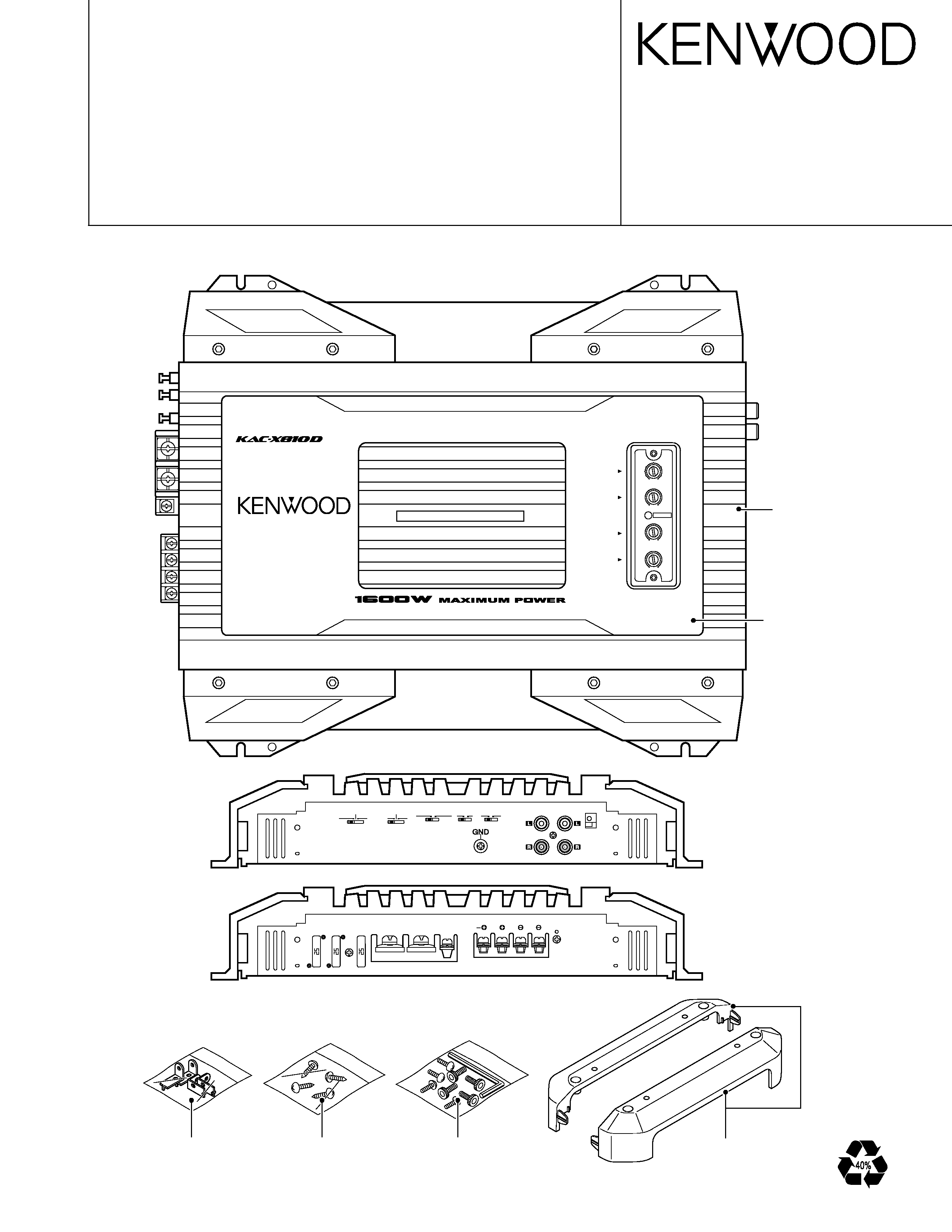
Screw set
(N99-1577-15)
Accessory
(W01-1586-05)
Cover
(F07-1110-01) x 2
Refer to the PARTS LIST
q KAC-X810D
OFF -12dB
-6dB
BAND REJECT
REMOTE +12dB
OFF
B.M.S
NORMAL REVERSE
15Hz 25Hz
OFF ON
PHASE
INFRASONIC
LINE IN
LINE OUT
EXT.AMP.CONT.
FUSE(25AX3)
BATT.
P.CON
SPEAKER
OUTPUT
POWER IN
GND
INPUT SENSITIVITY(V)
B.M.S. FREQUENCY(HZ)
LPF FREQUENCY(HZ)
B.R.F. FREQUENCY(HZ)
MONO POWER AMPLIFIER
e X celon
(MIN)5
0.2(MAX)
40
200
50
200
40
100
0.3
0.5
2
1
3
4
V-COLOR
Heat sink
(F01-1684-01)
Dressing panel
(A21-4190-02)
Mounting hardware
(J21-9864-04) x 4
KAC-X810D/PS810D
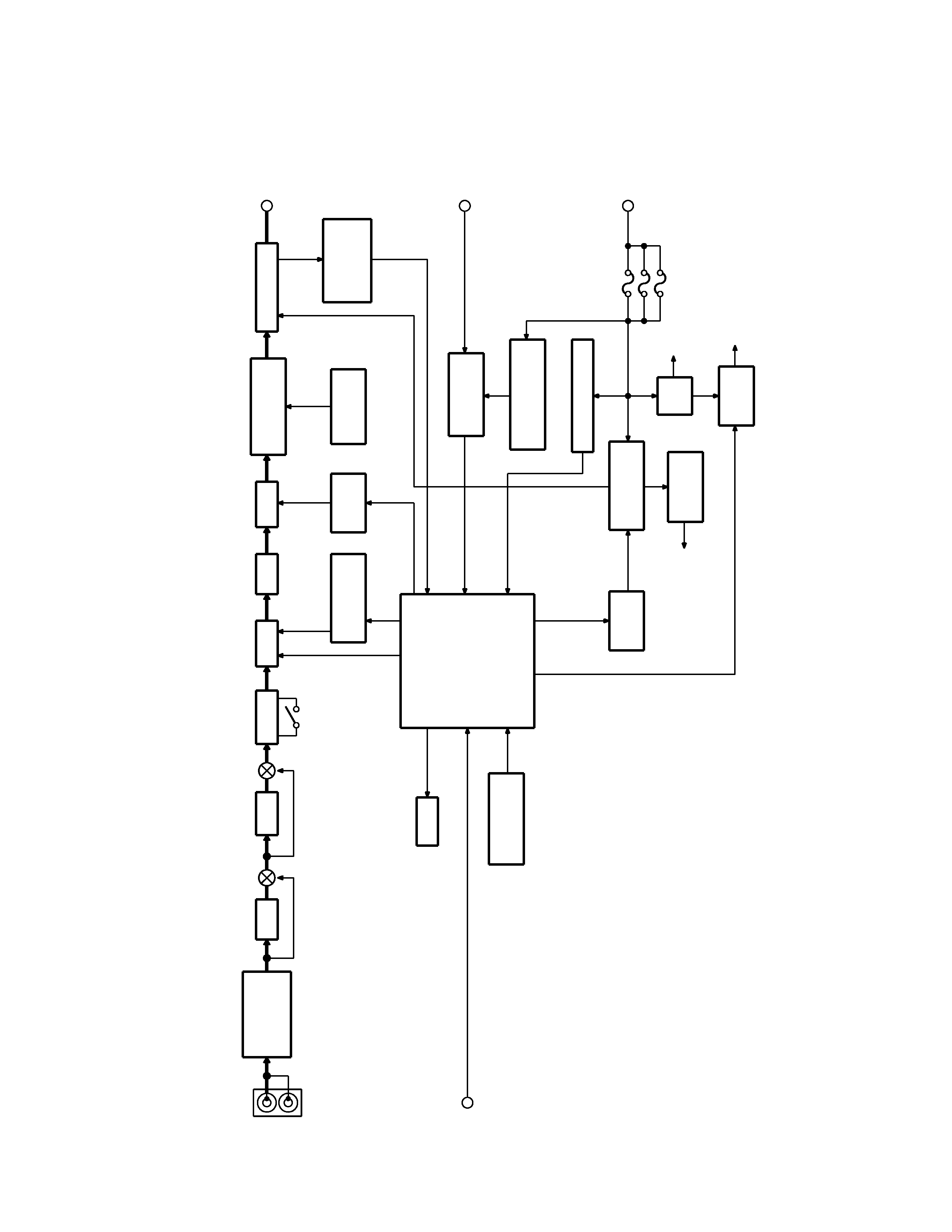
2
BLOCK
DIAGRAM
INPUT
OUTPUT
J1
ISOLATION
AMPLIFIER
INPUT SENS
I.S.F.
B.R.F
INV
S5
B.M.S
L.P.F
MUTE
AMP
COMPEARATE
POWER AMP
OFFSET
FREQUENCY
DRIVER
MUTE
TRIANGLE
WAVE
OVERLOAD
DETECTION
DC OFFSET
MICRO-COMPUTER
DETECTION
PCON
OVER VOLTAGE
PROTECTION
DOWN VOLTAGE
SWITCH
CONVERTER
DC/DC
+15V -15V
AVR
AVR
+5V
5V
SWITCH
POWER
FUSE
V-LED
PROTECTION
THERMAL
OUTPUT
SPEAKER
J2
J2
PCON
J2
BATTERY
J5
B.BOOST
CONTROL
IC1
IC2
IC3
IC3
IC4,13
IC7
Q6
IC8,9
Q53,56
IC12
IC8,9
Q4
IC15
IC6
D1
TH2,3
Q62,63
Q34-37
Q73
Q65
Q57,61
Q7
Q5
Q10,11
S3
S4
IC14
Q68,69
Q14-25,39-46
+5V
+5V
+15V
-15V
+B/-B/+14V
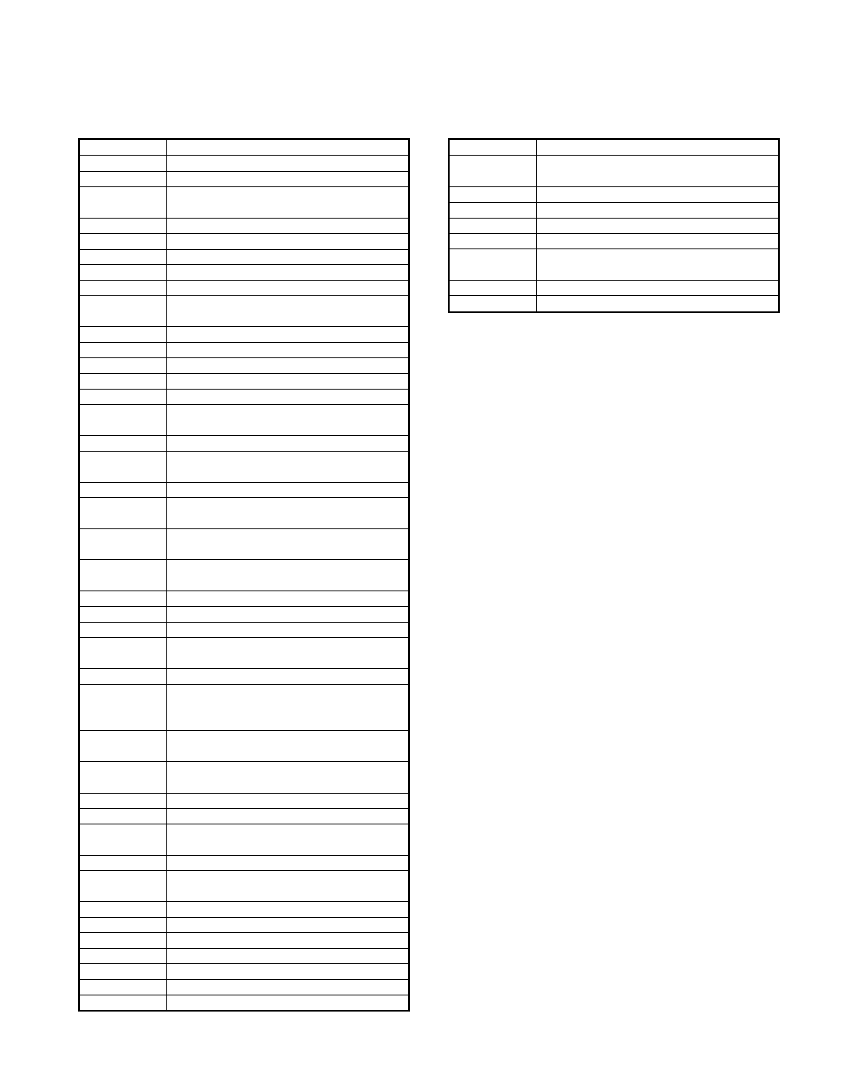
KAC-X810D/PS810D
3
q AUDIO UNIT (X09-5440-10)
Component
Purpose · Function
IC1
Isolation AMP
IC2
Infrasonic AMP
IC3
Band rejection AMP
(1/4-3/4)
IC3 (4/4)
Inverter
IC4,13
Bus boost AMP
IC5
Recet IC
IC6
Microcomputer
IC7
Low-pass filter AMP
IC8 (1/2)
Chopping wave generator circuit
IC9 (1/2)
IC8 (2/2)
Summing AMP
IC9 (2/2)
PWM waveform generator circuit
IC10,11
Dead time generator circuit
IC12
Used for overcurrent detection
IC14
DC/DC converter IC
IC15
Used for B.M.S frequency offset
Q59,60
Q1-3
Used for LED driver
Q4,6
Used for MUTE
D6,7
Q5
Used for SW +5V
Q7,9
Used for +5V AVR
D11
Q10,12
Used for +15V AVR
D14
Q11,13
Used for 15V AVR
D15
Q14,16-19
Used for VI conversion
Q15,D20
Used for +15V AVR
Q20,21
Used for cascade
Q22,24
Gate failure prevention circuit
D27
Q23,25
Used for D-AMP ON/OFF
Q26-29
Q34-37
MOS FET for DC/DC
Q68,69
Q30-33
MOS FET Driver Tr
Q39-42
Q38,58,64
Overcurrent Detector Circuit
D32,42,45,46
Q43-46
MOS FET (Power FET)
Q47-50
MOS FET Driver Tr
Q51,52
Used for output current VI conversion
Q54,55
Q53,56
DC detection
Q57,61
Used for P-CON
D33
Q62,63
Power ON
Q65,D34
Used for overvoltage detection
Q66
Used for B.M.S
Q70,71
Used for Pulling 15V
Q73,D37
Used for reduced voltage detection
D1
Variable color LED
D2-5
Used for static electricity prevention
COMPONENT DESCRIPTION
Component
Purpose · Function
D8-10,12,13
Used for the limitation of a
chopping wave voltage
D21,22,40,41
Used for rectification (±B)
D23-26
Used for rectification (+15V)
D28,29
Used for ±8.2V AVR
D30,31
Used for MOS FET Drive
D35,36,38
Protection circuit (error connection) for
the prevention of reverse connection
D39
Used for 5.1V AVR
D43,44
±10V AVR

KAC-X810D/PS810D
4
MICROCOMPUTER'S TERMINAL DESCRIPTION
q IC6 (AUDIO UNIT : X09-5440-10)
Pin No.
Pin Name
I/O
Description
Processing Operation
1
+5V_SW
O
Low-current control
Lo: SW 5V ON
2
N.C.
-
Not used
3
FAN
-
Not used
4
N.C.
-
Not used
5
D_VOLTAGE
I
D-class overvoltage detection
Lo: Overvoltage detection
6
V_DOWN
I
Reduced voltage detection
Hi: Reduced voltage detection
7
D_CURRENT
I
D-class overcurrent detection
Lo: Overcurrent detectction when D power ON
8
AB_VOLTAGE
I
AB-class overvoltage detection
Lo: Overvoltage detection
9
AB_CURRENT
I
AB-class overcurrent detection
Hi: Overcurrent detection
10
BLUE
O
Blue control of variable illumination
Hi: Illumination lighting
11
GREEN
O
Green control of variable illumination
Hi: Illumination lighting
12
RED
O
Red control of variable illumination
Hi: Illumination lighting
13
TEST
-
14
RST
-
Reset signal input
Lo: Reset operation
15
XIN
-
High-frequency oscillating connection pin
16
XOUT
-
High-frequency oscillating connection pin
17
VSS
-
0V (GND)
18
VAREF
-
A/D reference voltage
19
ADIN_1
I
Temperature detection 1 (A/D input)
Hi: Abnormal temperature detection
20
ADIN_2
I
Temperature detection 2 (A/D input)
Hi: Abnormal temperature detection
21
ADIN_3
I
Temperature detection 3 (A/D input)
Hi: Abnormal temperature detection
22
ADIN_4
I
Temperature detection 4 (A/D input)
Hi: Abnormal temperature detection
23
N.C.
-
Not used
24
BASS 12dB
I
B.M.S +12dB fixed
Hi: B.M.S fixed +12dB
25
BASS REMO
I
B.M.S switched from H/U
Hi: B.M.S switched from H/U
26
BASS OFF
I
BOOST OFF
Hi: BOOST OFF
27
D_POWER
O
D-class Amp block control
Hi: D-class Amp block ON
28
N.C.
-
Not used
29
N.C.
-
Not used
30
POWER
O
AMP power control
Hi: SW 14.4V ON
31
COM_HU
I
Pulse measurement of H/U communication
32
OFFSET CON
O
Offset control of BASS BOOST frequency
Hi: OFFSET ON
33
BASS_CON_A
O
BASS BOOST control A
34
BASS_CON_B
O
BASS BOOST control B
35
N.C.
-
Not used
36
N.C.
-
Not used
37
STANBY
I
Stop mode canceled by Pcon ON
Lo: Pcon ON or BUP overvoltage detection
38
N.C.
-
Not used
39
N.C.
-
Not used
40
VDD
-
Positive potential
41
TACT SW
I
Switch input for color determination
Hi: SW ON
42
MUTE2
O
Mute control in driver stage
Lo: MUTE2 ON
43
MUTE1
O
Mute control in amplifier block input stage
Lo: MUTE1 ON
44
N.C.
-
Not used
KAC-X810D/PS810D
5
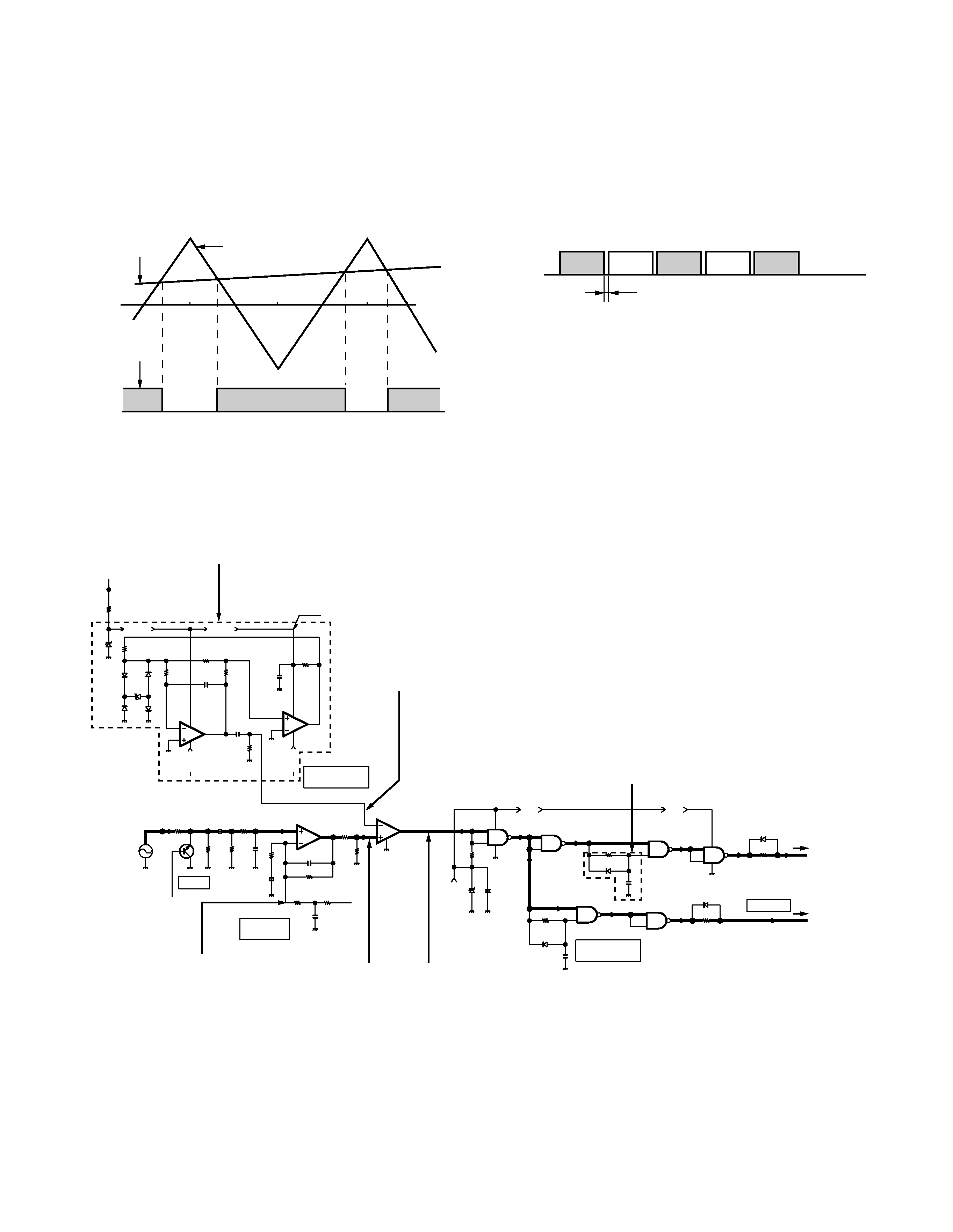
CIRCUIT DESCRIPTION
1. PWM Signal Waveform Generation
A and B are sent to the comparator so as to generate the
PWM waveform of C. (A clock of 50% in duty ratio is
obtained when B is 0.)
A: Chopping wave
B: Analog input
C: PWM Signal
A
B
C
0
0
UP
DOWN
UP
DOWN
UP
Dead Time
The waveform of C is divided into upper and lower gate
waveforms. An OFF section is created so that the upper
gate waveform is not turned on simultaneously with the
lower gate waveform.
MUTE
Q6
D12
D10
D13
D9
D43
D8
IC9
AMP
IC8
(2/2)
SUMMING
D39
(2/2)
IC11
D17
GEN CIRCUIT
DEAD TIME
(2/4)
(2/4)
(1/4)
IC10
IC10
IC10
(4/4)
IC10
(3/4)
D16
PWM WAVE
GEN CIRCUIT
(1/2)
IC9
IC8
(1/2)
IC11
D19
(1/4)
D18
VI CONV
4
1800P
R58
33K
10.3V
8
3
2
150
+10.3V
R77
820
R86
4.7K
R270
C57 47P
R100 680K
47u
10V
68K
C58
3900P
+
C49
R101
+
R71
3.3K
82K
R75
C47
0.1
C42
1u50
R78
1K
6
R83
1K
5
24K
R107
5
4
R108
1.5K
R105
4.7K
7
3
6
12
C55
39P
12
13
C36
47u10
+
10K
R85
2
510
R66
7
1
14
6
5
4
3
11
C54
13
12
11
39P
R84 10K
10
9
8
C62
0.01
IC9(2/2)
R106
10K
10.3V
1
C59
0.01
9
11
10
8
7
R70
10K
R69
C56
3K
+10.3V
R73
1.5K
7
R119
1K
14
10
9
8
R118
1K
+5V
+5V
+5V
10.3V
C
B
Analog-fed back from
the output stage.
Audio
signal
Chopping wave generator circuit
The dead time is determined by
this time constant.
Upper gate
Lower gate
A