In compliance with Federal Regulations, following are reproduc-
tions of labels on, or inside the product relating to laser product
safety.
KENWOOD-Corp. certifies this equipment conforms to DHHS
Regulations No. 21 CFR 1040. 10, Chapter 1, Subchapter J.
DANGER : Laser radiation when open and interlock defeated.
AVOID DIRECT EXPOSURE TO BEAM.
MULTIPLE VIDEO CD PLAYER
DPF-K6010V
SERVICE MANUAL
© 1998-8/B51-5471-00 (K/K) 399
i
I
È
0
73
4
¢
8
PAL
NTSC
L
R
1
1
S -VIDEO
2
2
VARIABLE
AUDIO OUTPUT
VIDEO OUTPUT
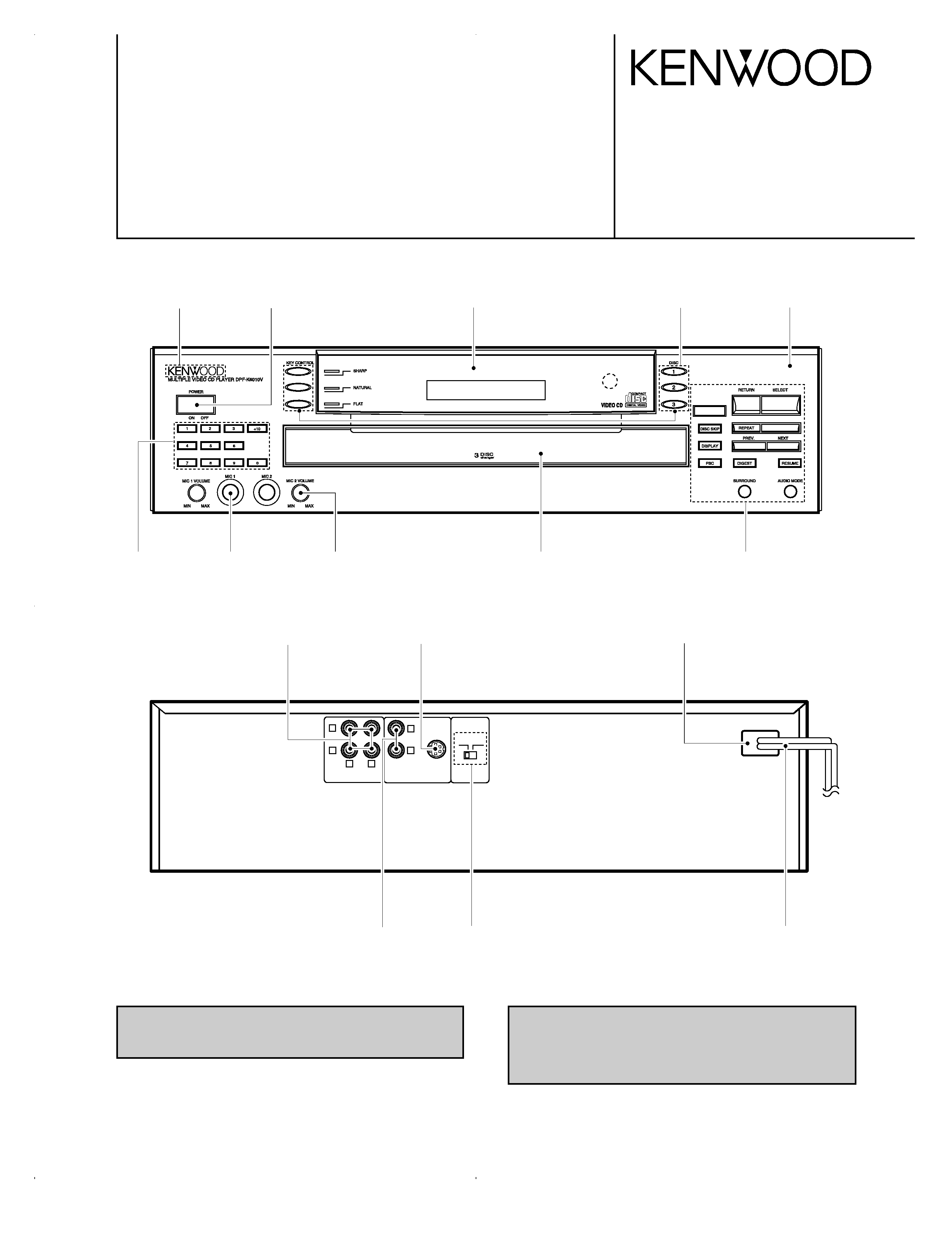
Panel *
(A60-)
Knob
(K29-7354-14)
Knob
(K29-7352-03)
Panel (CD)
(A29-1016-02)
Phone jack
(E11-0224-05)
Phono jack
(E63-0120-05)
Cylindrical receptacle
(E56-0014-05)
Power cord bushing
(J42-0083-05)
AC power cord *
(E30-)
Slide switch
(S31-2132-05)
Phono jack
(E63-0128-05)
Knob
(K29-7351-03)
Knob
(K29-7353-02)
Front glass
(B10-3403-03)
Knob
(K27-2178-04)
KENWOOD badge
(B43-0302-04)
* Refer to parts list on page 25.
· Refer to page 12 between Adjustment and Pc
board if you want to know CD mechanism
exploded View.
DPF-K6010V(K)COVER1,1( 98.12.1010:54 y[W 2
Audio
(E30-0505-05)
(E30-1427-05)
(E03-0115-05)
(A70-1226-05) : RC-P0610
Battery cover (A09-1104-08)
cord .................. (1)
Remote control unit ............. (1)
Batteries (R03/AAA) ........ (2)
Video cord ................... (1)
AC plug adaptor ............. (1)
Use to adapt the plug on the power cord
to the shape of the wall outlet.
(Accessory only for regions where
use is necessary.)
VOLUME
REMOTE
CONTROL
UNIT
RC-P0610
DISC
KEY
CONTROL
1
2
3
0
SLOW
8
7
RETURN
E
SURROUND
ECHO
+
-
GAME
ZOOM
1
AUDIO
MODE
2
3
4
5
6
7
8
9
0
+10
PBC
DISPLAY
RESUME
TIME
P.MODE
DIGEST
MEMORY
REPEAT
CLEAR
A-B
REPEAT
4
/PREV.
NEXT/
¢
¡
1
3
/SELECT
RANDOM
i
I
È
DPF-K6010V
2
CONTENTS / ACCESSORIES / CAUTIONS
CONTENTS / ACCESSORIES / CAUTIONS.............2
DISASSEMBLY FOR REPAIR...................................3
BLOCK DIAGRAM .....................................................4
CIRCUIT DESCRIPTION ...........................................5
ADJUSTMENT ........................................................ 10
EXPLODED VIEW ...................................................12
PC BOARD ..............................................................13
SCHEMATIC DIAGRAM ..........................................17
EXPLODED VIEW ...................................................24
PARTS LIST.............................................................25
SPECIFICATIONS .....................................Back cover
Contents
Accessories
Before transporting or moving this unit, carry out the following
operations.
1. Turn the unit ON but do not load a disc.
2. Wait a few seconds and verify that the display shown appears.
3. Wait until "no disc" is displayed and turn off the unit.
Note related to transportation and move-
ment
nnO dI SC
:
Operation to reset
The microcomputer may malfunction (impossibility to operate,
erroneous display, etc.) when the connection cords are un-
plugged while the unit is ON or due to an external factor. In this
case, execute the following method to reset the microcomputer
and return it to normal condition.
¶ Please be aware that resetting the unit will erase all stored informa-
tion and return it to the factory settings.
Set the POWER switch to OFF, and after several seconds,
set the POWER switch back to ON.
Cautions
DPF-K6010V(K)COVER1,1( 98.12.1010:54 y[W 3
DPF-K6010V
3
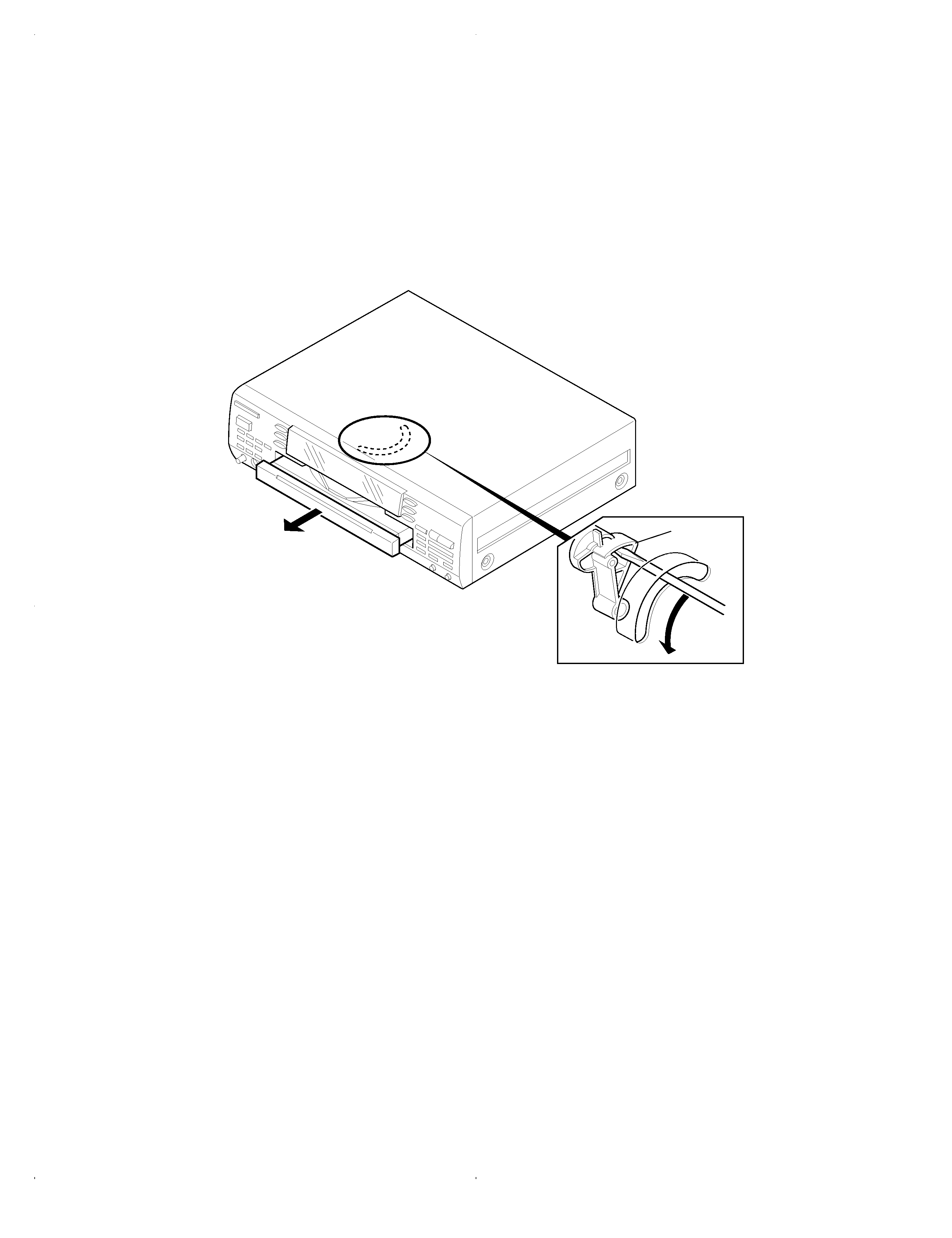
DISASSEMBLY FOR REPAIR
REAR
SIDE
Friction
Arm
How to open the tray if not comes out.
(1) From the rear side of the CD mechanism, use a screw driver or the like to turn the friction arm fully counterclockwise.
(2) Pull out the tray front wards by hand when the tray comes just out.
* As for details of items in the below, refer to RXD-F3 service manual (B51-5091-00).
(1) How to detach the tray.
(2) How to attach the tray.
(3) Replacing the pickup.
DPF-K6010V(K)COVER1,1( 98.12.1010:54 y[W 6
(CDM-27)
(D40-1562-15)
(X25- )
DPF-K6010V
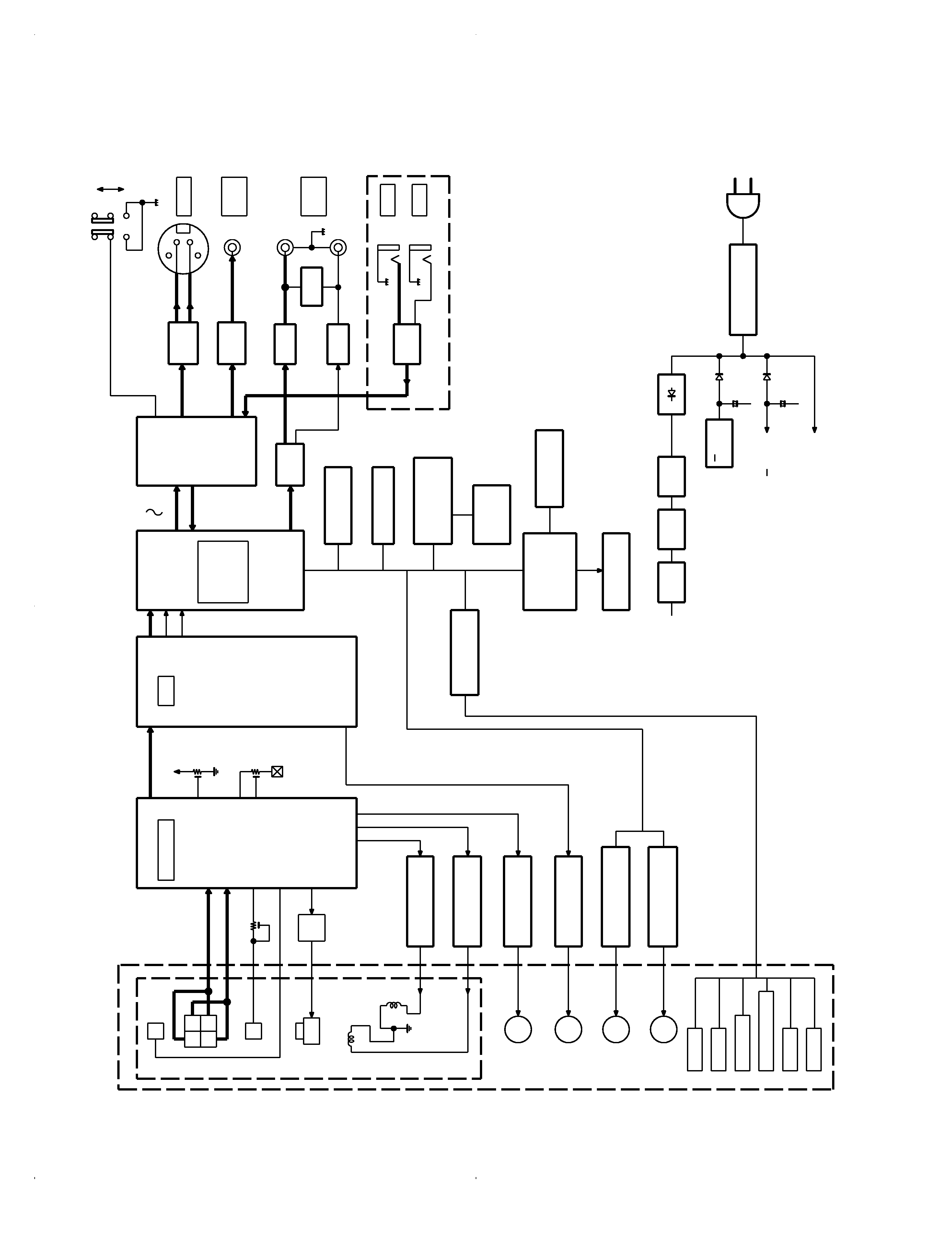
PD1
PD2
E
F
LD
FEO
TA
O
SLO
RF
FEI
TEO
VR1
F. B
MDP
RF
C4M
SQCK
DATA
XTAI
VR2
TE-B
TRACKING
COIL
FOCUS
COIL
VR3
T. G
TEI
DATA
LRCK
LRCK
BCK
BCK
YUV7
YUV0
A IN
MIC1/2
A OUT
NTSC
PAL
Lch
Rch
RMR/RMF/BRKM
Y
C
+9.5V
F
AB
DC
E
LD
SW
IC1 CXA1782BQ
RF/SERVO
DRIVER
FOCUS COIL
IC3 (1/6)
TRACKING COIL
DRIVER
IC3 (2/6)
FEED MOTOR
DRIVER
IC3 (3/6)
DISC MOTOR
DRIVER
IC3 (4/6)
ROTARY TRAY
DRIVER
LOADING MOTOR
DRIVER
DSP
IC2 CXD2500BQ
M
M
M
M
PICKUP
Q2,3
LD
BA6198S
IC3 (5/6)
IC3 (6/6)
M3 LOADING MOTOR
M4 ROTARY MOTOR
M1 DISC MOTOR
M2 FEED MOTOR
IC11 ES3210F
FL DRIVER
u-COM
CONTROL/
MPEG/
IC12 ES3209F
VIDEO
ENCODER
AUDIO
D.A.C
IC8
Q31
VIDEO
AMP
Q32,33
AMP
VIDEO
S1
S OUT
VIDEO
OUT
J3
J2
L.P.F
IC9 (1/2)
L.P.F
IC9 (2/2)
MUTE
J1
OUT
AUDIO
MIC
AMP
IC1
J1
J2
MIC1
MIC2
HM514260
4M DRAM
IC13
4M ROM
IC14
LOGIC
PROGRAMMED
IC16
DIVIDER
SENSOR
REMOTE
CONTROL
A1
I/O EXPANDER
74HC166
IC17
FL DISPLAY
6-BT-267GK
FL DRIVER
uPD16311
IC2
KEY MATRIX
+3.3V
AVR
IC15
SL SW
LD SW
UP/DOWN SW
UNLD SW
PS SW
ST SW
+5.0V
AVR
Q14
+6.5V
AVR
IC5
24.0V
AVR
Q13
D38
D36
D37
12.7V
AC
F1,2
TRANSFORMER
AC IN
DPF-K6010V
4
BLOCK
DIAGRAM
DPF-K6010V(K)
COVER1,1(
98.12.10
10:54
y[W
7
DPF-K6010V
No.
Name
I/O
Description
1
VDD
Voltage supply for 3.3V.
2
RAS
O
DRAM row address strobe (active low).
3
DWE
O
DRAM write enable (active low).
4~12
MA0~MA8
O
DRAM multiplexed row and column address bus.
13~28
DBUS0~DBUS15
I/O
DRAM data bus.
29
RESET
I
System reset (active low).
30
VSS
Ground.
31
VDD
Voltage supply for 3.3V.
32~39
YUV0~YUV7
O
Y is luminance, UV are chrominance data bus for screen
Video interface. YUV (0~7) for 8 bit YUV mode.
40
VSYNC
I/O
Vertical sync for screen video interface, programmable for rising or falling edge.
41
HSYNC
I/O
Horizontal sync for screen video interface, programmable for rising or falling edge.
42
CPUCLK
I
RISC and system clock input.
CPUCLK is used only if SEL PLL [1 : 0] = 00.
43
PCLK2X
I/O
Pixel clock ; two times the actual pixel clock for screen video interface.
44
PCLK
I/O
Pixel clock qualifier in for screen video interface.
45
(GFS) AUX0
I/O
GFS input from IC2 (CXD2500BQ).
46
(SQSO) AUX1
I/O
Inputs 80 bit Sub Q and 16 bit PCM peak-level data.
47
(VFD D) AUX2
I/O
Auxiliary control pins.
48
(MUTE) AUX3
I/O
"H" for muting, "L" for release.
49
(IRQ) AUX4
I/O
Auxiliary control pins.
50
VSS
Ground.
51
VDD
Voltage supply for 3.3V.
52
VFD L
I/O
Auxiliary control pins.
53
STB
I/O
Auxiliary control pins.
54
VFD CK
I/O
Auxiliary control pins.
55~62
LD0~LD7
I/O
RISC interface data bus.
63
LWR
O
RISC interface write enable (active low).
64
LOE
O
RISC interface output enable (active low).
65~67
LCS (3, 1, 0)
O
RISC interface chip select (active low).
68~79
LA0~LA11
O
RISC interface address bus.
80
VSS
Ground.
81
VPP
Digital supply voltage for 5V.
82~87
LA12~LA17
O
RISC interface address bus.
88
ACLK
I/O
Master clock for external audio DAC (8.192MHz, 11.2896MHz, 12.288MHz, 16.9344
MHz, and 18.432MHz).
O
Dual-purpose pin. AOUT is the audio interface serial data output
Pins SEL PLL [1 : 0] select phase-lock loop (PLL) clock frequency CPUCLK for the
ES3210 :
00 = bypass PLL.
89
AOUT/SEL PLL0
I
01 = 54MHz PLL.
10 = 67.5MHz PLL.
11 = 81MHz PLL.
90
ATCLK
I/O
Audio transmit bit clock.
O
Dual-purpose pin. ATFS is the audio interface transmit frame sync.
91
ATFS/SEL PLL1
I
Pins SEL PLL [1 : 0] select phase-lock loop (PLL) clock frequency CPUCLK for the
ES3210. See the SEL PLL0 pin above for the settings.
92
DOE
O
DRAM output enable (active low).
93
AIN
I
Audio interface serial data input.
94
ARCLK
I
Audio receive bit clock.
95
ARFS
I
Audio interface receive frame sync.
96
TD MCLK
I
TDM interface serial clock.
97
TD MDR
I
TDM interface serial data receive.
98
TD MFS
I
TDM interface frame sync.
99
CAS
O
DRAM column address strobe bank 0 (active low).
100
VSS
Ground.
5
CIRCUIT DESCRIPTION
1. MPEG Microprocessor : IC11 (E3210F)
Pin description
DPF-K6010V(K)COVER1,1( 98.12.1010:54 y[W 10