PD-42V475/S
PD-42V485/S
SCHEMATIC DIAGRAMS
COPYRIGHT © 2004 Victor Company of Japan, Limited
No.YA099
2004/7
PDP COLOR TELEVISION
CD-ROM No. SML20040
8
BASIC C
FP2
HASSIS
POWER
DISPLAY
SLEEP TIMER
LIGHT
FREEZE
THEATER PRO
VIDEO STATUS
1
7
4
TUNE
3
9
6
RETURN+
MUTING
MENU
OK
BACK
2
8
0
5
CH +
VOL
Ð
VOL
+
REC
OPEN/CLOSE
STILL/PAUSE
STOP
PAUSE
PLAY
FF
REW
TV CATV VCR DVD
VCR CHANNEL
PREV NEXT
TV/VCR
VCR/DVD
POWER
SOUND
CH Ð
TV
RM-C1257G
ASPECT
INDEX
SWAP
SELECT
MULTI SCREEN
INPUT
C.C.
TWIN
No. YA099
2-1
1. SAFETY
The components identified by the
symbol and shading
are critical for safety. For continued safety replace safety
critical components only with manufactures recommended
parts.
2. SPECIFIED VOLTAGE AND WAVEFORM VALUES
The voltage and waveform values have been measured under
the following conditions.
(1)Input signal
: Colour bar signal
(2) Setting positions of each knob/button and
variable resistor
: Original setting position when
shipped
(3)Internal resistance of tester : DC 20k
/V
(4)Oscilloscope sweeping time : H
20µs/div
:V
5ms/div
: Others
Sweeping time is
specified
(5)Voltage values
: All DC voltage values
Since the voltage values of signal circuit vary to some extent
according to adjustments, use them as reference values.
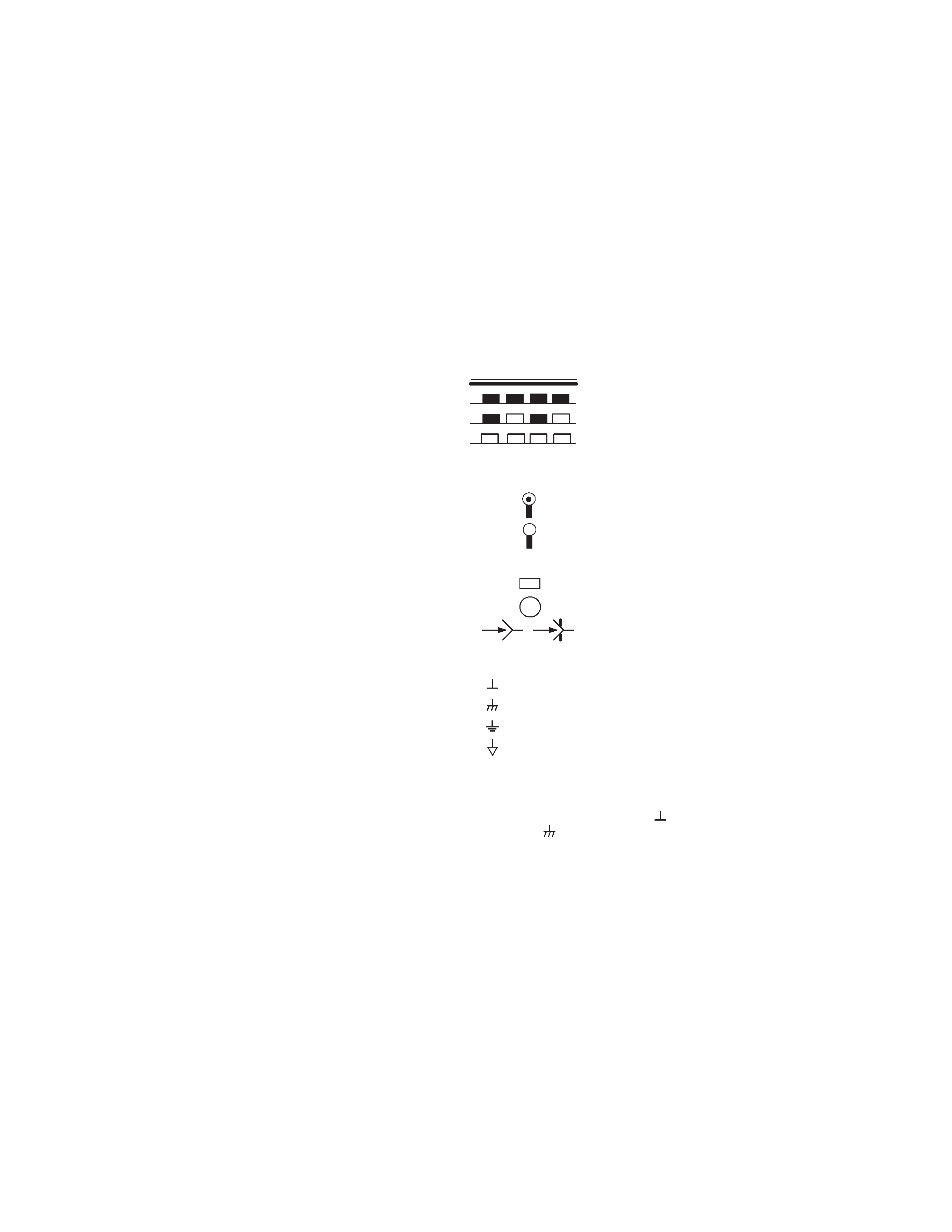
3. INDICATION OF PARTS SYMBOL [EXAMPLE]
·In the PW board
: R1209
R209
4. INDICATIONS ON THE CIRCUIT DIAGRAM
(1) Resistors
·Resistance value
No unit
: [
]
k: [k
]
M: [M
]
·Rated allowable power
No indication
: 1/16 [W]
Others
: As specified
·Type
No indication
: Carbon resistor
OMR
: Oxide metal film resistor
MFR
: Metal film resistor
MPR
: Metal plate resistor
UNFR
: Uninflammable resistor
FR
: Fusible resistor
Composition resistor 1/2 [W] is specified as 1/2S or Comp.
(2) Capacitors
·Capacitance value
1 or higher
: [pF]
less than 1
: [µF]
·Withstand voltage
No indication
: DC50[V]
AC indicated
: AC withstand voltage [V]
Others
: DC withstand voltage [V]
Electrolytic Capacitors
47/50[Example] : Capacitance value [µF]/withstand voltage[V]
·Type
No indication
: Ceramic capacitor
MY
: Mylar capacitor
MM
: Metalized mylar capacitor
PP
: Polypropylene capacitor
MPP
: Metalized polypropylene capacitor
MF
: Metalized film capacitor
TF
: Thin film capacitor
BP
: Bipolar electrolytic capacitor
TAN
: Tantalum capacitor
(3) Coils
No unit
: [µH]
Others
: As specified
(4) Power Supply
:B1
: B2(12V)
:9V
:5V
Respective voltage values are indicated
(5) Test point
: Test point
: Only test point display
(6) Connecting method
: Connector
: Wrapping or soldering
: Receptacle
(7) Ground symbol
: LIVE side ground
: ISOLATED(NEUTRAL) side ground
: EARTH ground
: DIGITAL ground
5. NOTE FOR REPAIRING SERVICE
This model's power circuit is partly different in the GND. The difference
of the GND is shown by the LIVE : (
) side GND and the ISOLATED
(NEUTRAL) : (
) side GND. Therefore, care must be taken for the
following points.
(1)Do not touch the LIVE side GND or the LIVE side GND and the
ISOLATED (NEUTRAL) side GND simultaneously. If the above
caution is not respected, an electric shock may be caused.
Therefore, make sure that the power cord is surely removed
from the receptacle when, for example, the chassis is pulled
out.
(2)Do not short between the LIVE side GND and ISOLATED
(NEUTRAL) side GND or never measure the LIVE side GND and
ISOLATED (NEUTRAL) side GND at the same time with a measuring
apparatus (oscilloscope, etc.). If the above precaution is not
respected, a fuse or any parts will be broken.
Since the circuit diagram is a standard one, the circuit
and circuit constants may be subject to change for
improvement without any notice.
NOTE
Due improvement in performance, some part numbers
show in the circuit diagram may not agree with those
indicated in the part list.
When ordering parts, please use the numbers that
appear in the Parts List.
PD-42V475/S, PD-42V485/S
STANDARD CIRCUIT DIAGRAM
NOTE ON USING CIRCUIT DIAGRAMS

No. YA099
2-2
CONTENTS
USING P.W. BOARD .......................................................................................................................................... 2-3
SEMICONDUCTOR SHAPES ....................................................................................................................... 2-3
WIRING & MAIN PARTS LOCATION ....................................................................................................... 2-5
BLOCKDIAGRAM ............................................................................................................................................... 2-7
CIRCUITDIAGRAMS
RECEIVER PWB CIRCUIT DIAGRAM ................................................................................................................... 2-9
ANALOG SIGNAL PWB CIRCUIT DIAGRAM .................................................................................................... 2-11
AV JACK PWB CIRCUIT DIAGRAM ................................................................................................................... 2-21
DIGITAL SIGNAL PWB CIRCUIT DIAGRAM ..................................................................................................... 2-23
INTERFACE PWB CIRCUIT DIAGRAM .............................................................................................................. 2-45
AUDIO PWB CIRCUIT DIAGRAM ....................................................................................................................... 2-49
FRONT CONTROL PWB CIRCUIT DIAGRAM .................................................................................................. 2-51
FRONT LED PWB CIRCUIT DIAGRAM .............................................................................................................. 2-53
TEMP. SENSOR PWB CIRCUIT DIAGRAM ....................................................................................................... 2-54
REGULATOR PWB CIRCUIT DIAGRAM ............................................................................................................ 2-55
LINE FILTER PWB CIRCUIT DIAGRAM ............................................................................................................. 2-57
MAIN POWER PWB CIRCUIT DIAGRAM .......................................................................................................... 2-59
SUB POWER PWB CIRCUIT DIAGRAM ............................................................................................................ 2-65
PATTERNDIAGRAMS
RECEIVER PWB PATTERN .................................................................................................................................. 2-67
ANALOG SIGNAL MAIN PWB PATTERN .......................................................................................................... 2-69
AV JACK PWB PATTERN ..................................................................................................................................... 2-71
DIGITAL SIGNAL PWB PATTERN ...................................................................................................................... 2-73
INTERFACE PWB PATTERN ................................................................................................................................ 2-77
AUDIO PWB PATTERN ......................................................................................................................................... 2-78
FRONT CONTROL PWB PATTERN .................................................................................................................... 2-79
TEMP. SENSOR PWB PATTERN ......................................................................................................................... 2-80
FRONT LED PWB PATTERN ................................................................................................................................ 2-80
REGULOTOR PWB PATTERN ............................................................................................................................. 2-81
LINE FILTER PWB PATTERN .............................................................................................................................. 2-83
SUB POWER PWB PATTERN ............................................................................................................................. 2-84
MAIN POWER PWB PATTERN ............................................................................................................................ 2-85
VOLTAGE CHART ............................................................................................................................................. 2-89
WAVEFORMS ....................................................................................................................................................... 2-92
No. YA099
2-3
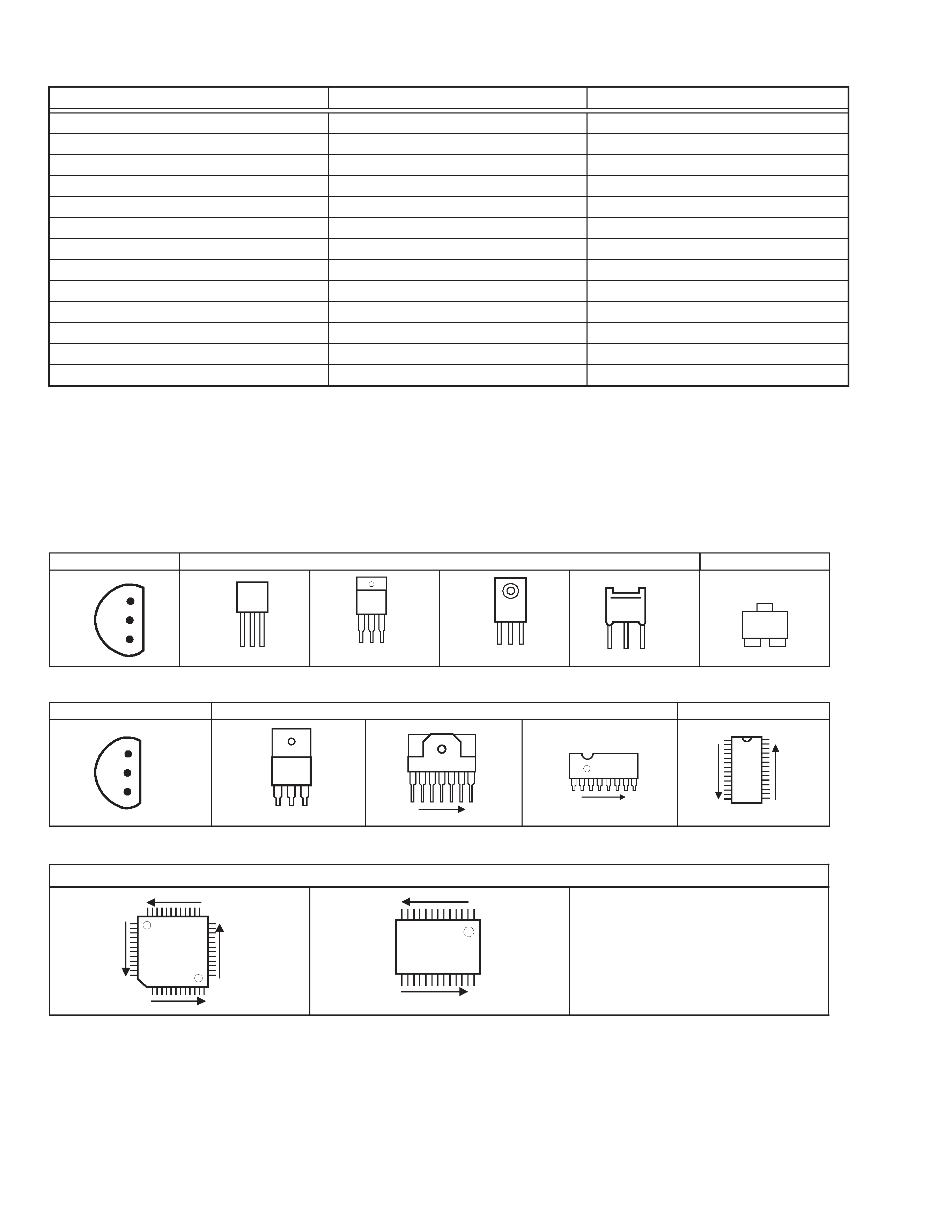
SEMICONDUCTOR SHAPES
USING P.W. BOARD
RECEIVER P.W. BOARD
SFP0F502A-M2
ANALOG SIGNAL P.W. BOARD
SFP0A503A-M2
AV JACK P.W. BOARD
SFP0J502A-M2
DIGITAL SIGNAL P.W. BOARD
SFP0D503A-M2
SFP0D504A-M2
INTERFACE P.W. BOARD
SFP-7505A-M2
SFP-7506A-M2
AUDIO P.W. BOARD
SFP-6004A-M2
FRONT CONTROL P.W. BORAD
SFP-8502A-M2
FRONT LED P.W. BOARD
SFP-8504A-M2
TEMP. SENSOR P.W. BOARD
SFP0T201A-M2
REGULATOR P.W. BOARD
SFP-9203A-M2
LINE FILTER P.W. BOARD
SFP-9510A-M2
MAIN POWER P.W. BOARD
SFP-9504A-M2
SUB POWER P.W. BOARD
SFP-9506A-M2
BOTTOM VIEW
FRONT VI EW
TOP VIEW
CHIP TR
IC
BOTTOM VIEW
FRONT VI EW
TOP VIEW
CHIP IC
TOP VIEW
1
N
N
1
OUT
E
IN
IN
OUT
E
1
N
N
1
N
N
N
1
N
E
C
B
EC B
C
BE
BC E
(G)(D)(S)
EC B
EC B
PWB ASS'Y NAME
PD-42V475/S
PD-42V485/S

No. YA099
2-4