No. 56084
2-1
AV-14F1P
SCHEMATIC DIAGRAMS
COLOR TELEVISION
AV-14F1P(PH)
COPYRIGHT
© 2000 VICTOR COMPANY OF JAPAN, LTD.
No. 56084
Sep. 2000
AV-14F1P
+
-

2-2
No. 56084
AV-14F1P
No. 56084
2-3
AV-14F1P
STANDARD CIRCUIT DIAGRAM
s NOTE ON USING CIRCUIT DIAGRAMS
1. SAFETY
The components identified by the !
!
!
!
! symbol and shading are
critical for safety. For continued safety replace safety critical
components only with manufactures recommended parts.
2. SPECIFIED VOLTAGE AND WAVEFORM VALUES
The voltage and waveform values have been measured under the
following conditions.
(1) Input signal
: Color bar signal
(2) Setting positions of each knob/button and variable resistor
: Original setting position when
shipped
(3) Internal resistance of tester : DC 20k
/V
(4) Oscilloscope sweeping time : H
© 20
µS/div
: V
© 5mS/div
: Others © Sweeping time is
specified.
(5) Voltage values
: All DC voltage values
* Since the voltage values of signal circuit vary to some extent
according to adjustments, use them as reference values.
3. INDICATION OF PARTS SYMBOL [EXAMPLE]
q In the PW board
: R1209 © R209
4. INDICATIONS ON THE CIRCUIT DIAGRAM
(1) Resistors
q Resistance value
No unit
: [
]
K: [K
]
M
: [M
]
q Rated allowable power
No indication
: 1/4 [W]
Others
: As specified
q Type
No indication
: Carbon resistor
OMR
: Oxide metal film resistor
MFR
: Metal film resistor
MPR
: Metal plate resistor
UNFR
: Non-flammable resistor
FR
: Fusible resistor
* Composition resistor 1/2 [W] is specified as 1/2S or Comp.
(2) Capacitors
q Capacitance value
1 or higher
: [pF]
less than 1
: [
µF]
q Withstand voltage
No indication
: DC50 [V]
AC indicated
: AC withstand voltage [V]
Others
: DC withstand voltage [V]
* Electrolytic Capacitors
47/50 [Example]: Capacitance value [
µF]/withstand voltage [V]
q Type
No indication
: Ceramic capacitor
MY
: Mylar capacitor
MM
: Metalized mylar capacitor
PP
: Polypropylene capacitor
MPP
: Metalized polypropylene capacitor
MF
: Metalized film capacitor
TF
: Thin film capacitor
BP
: Bipolar electrolytic capacitor
TAN
: Tantalum capacitor
(3) Coils
No unit
: [
µH]
Others
: As specified
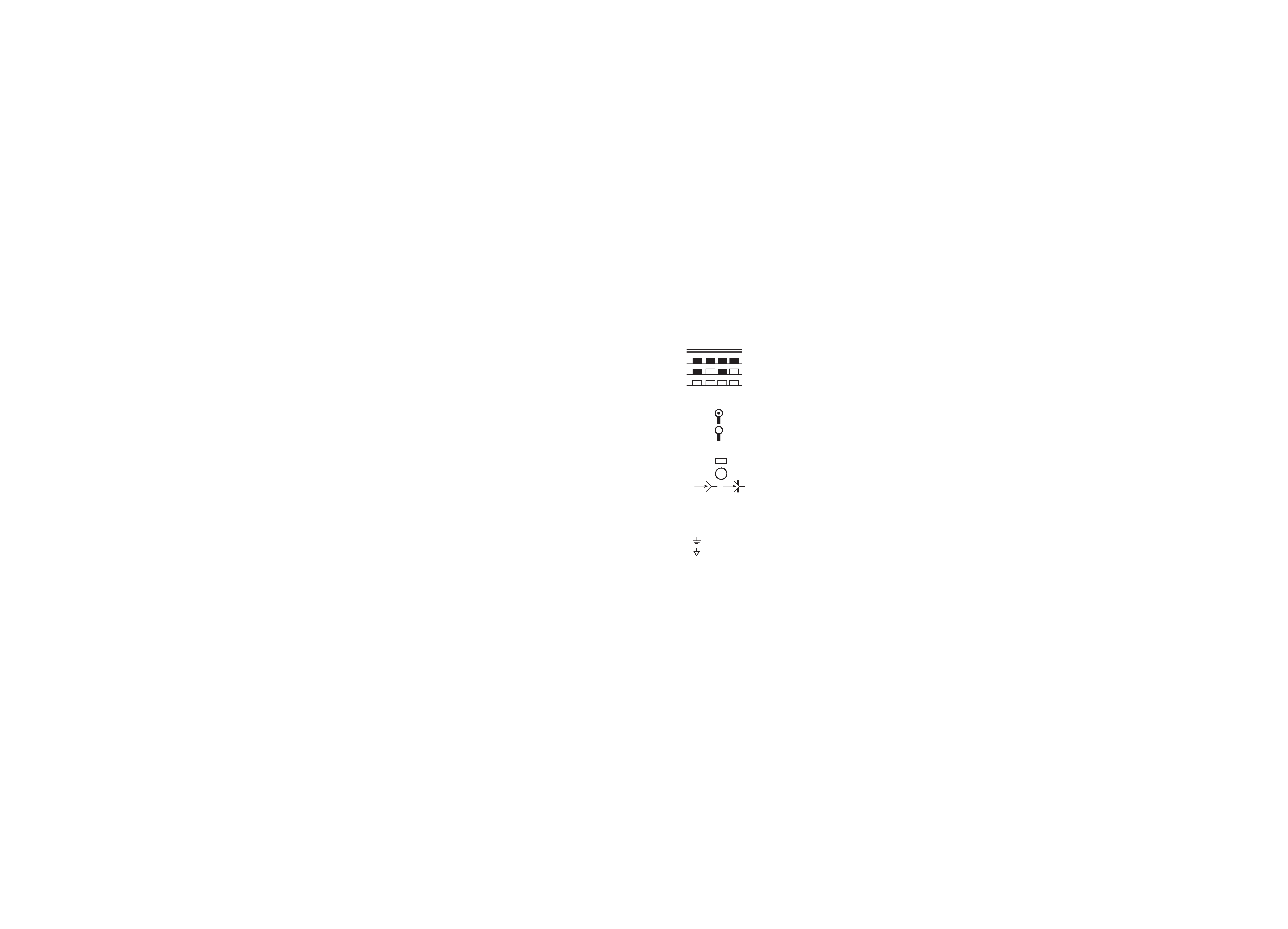
(4) Power Supply
: B1
: 12V
: 9V
: 5V
* Respective voltage values are indicated.
(5) Test point
: Test point
: Only test point display
(6) Connecting method
: Connector
: Wrapping or soldering
: Receptacle
(7) Ground symbol
#
: LIVE side ground
"
: ISOLATED (NEUTRAL) side ground
: EARTH ground
: DIGITAL ground
5. NOTE FOR REPAIRING SERVICE
This model's power circuit is partly different in the GND. The differ-
ence of the GND is shown by the LIVE : (#) side GND and the
ISOLATED (NEUTRAL) : (") side GND. Therefore, care must be
taken for the following points.
(1) Do not touch the LIVE side GND or the LIVE side GND and the
ISOLATED (NEUTRAL) side GND simultaneously. If the above
caution is not respected, an electric shock may be caused.
Therefore, make sure that the power cord is surely removed from
the receptacle when, for example, the chassis is pulled out.
(2) Do not short between the LIVE side GND and ISOLATED (NEU-
TRAL) side GND or never measure with a measuring apparatus
(oscilloscope, etc.) the LIVE side GND and ISOLATED (NEU-
TRAL) side GND at the same time. If the above precaution is
not respected , a fuse or any parts will be broken.
q Since the circuit diagram is a standard one, the circuit and
circuit constants may be subject to change for improvement
without any notice.
2-4
No. 56084
AV-14F1P
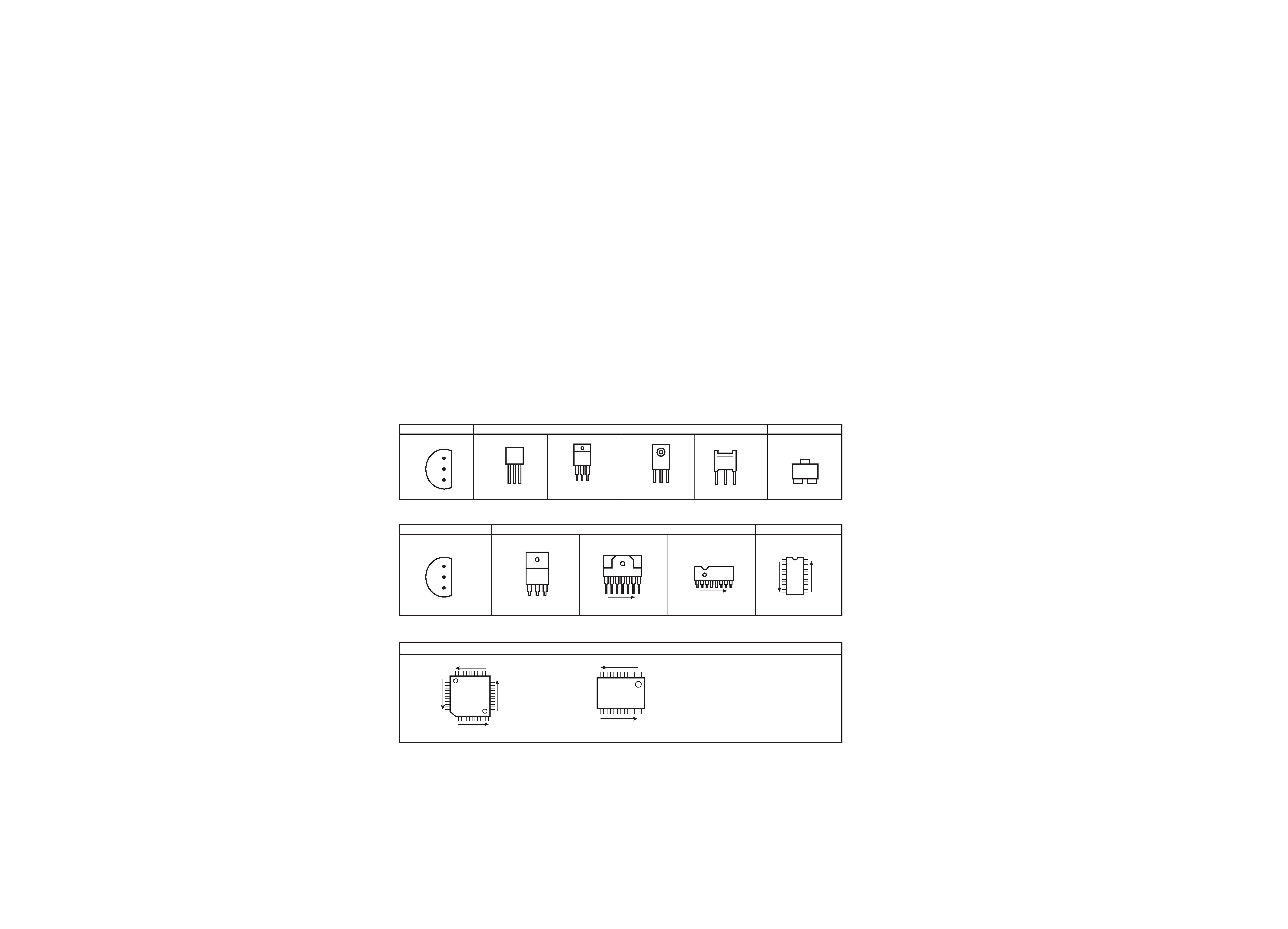
E CB
E
CB
IN E OUT
1N
1N
1N
OUT
E
IN
E
C
B
TOP VIEW
FRONT VIEW
TOP VIEW
BOTTOM VIEW
IC
CHIP IC
TOP VIEW
CHIP TR
FRONT VIEW
BOTTOM VIEW
TRANSISTOR
E CB
B
(G)
C
(D)
E
(S)
C
BE
N
N
N
1
N
1
N
SEMICONDUCTOR SHAPES
CONTENTS
SEMICONDUCTOR SHAPES ........................................................... 2-4
BLOCK DIAGRAM ............................................................................ 2-5
CIRCUIT DIAGRAMS
MAIN PWB CIRCUIT DIAGRAM (Including CRT SOCKET PWB) ......................................... 2-7
PATTERN DIAGRAMS
MAIN PWB PATTERN ............................................................................................................. 2-11
CRT SOCKET PWB PATTERN ............................................................................................... 2-13
No. 56084
No. 56084
2-6
2-5
AV-14F1P
AV-14F1P
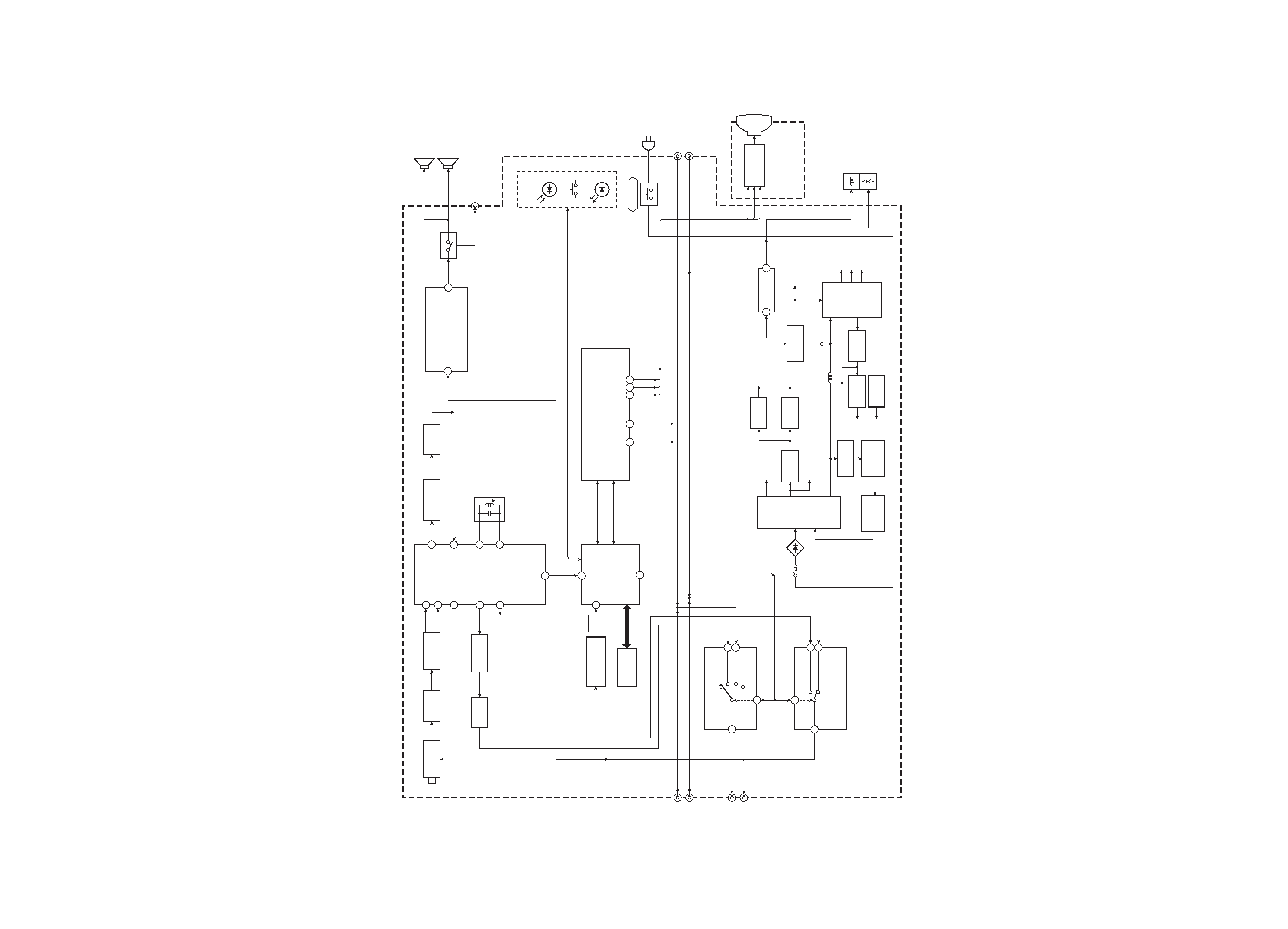
BLOCK DIAGRAM
TUNER
MAIN PWB
Q101
IC701
MICRO
COMPUTER
IC201
V/C DEF.
PROCESSOR
IF
OSD
T921
SW
TRANSF.
SCL,SDA
4
5
3
REMOCON
RECEIVER
SCL
SDA
VIDEO
LOW-B SW
IC941
ERROR AMP
Q522
T522
HVT
(FBT)
H.OUT
TP-91(B1)
H.OUT
H.OUT
CRT SOCKET
PWB
VERT.OUT
V.OUT
V.OUT
PC921
VOLTAGE
FEEDBACK
IC921
POWER
REG
FOCUS
SCREEN
ANODE
KEY
LED
R.G.B. OUT
V. DY
H. DY
B
G
R
V01
CRT
AC IN
VIDEO
FRONT IN
VIDEO IN
AUDIO IN
H.
OUT
V.
OUT
F901
POWER SW
Q351~Q353
RESET
5V REG & RESET
SF101
CF131
SAW FILTER
4.5MHz TRAP
IF AMP
VIF IN
VIF IN
RF AGC
OUT
V OUT
TV.M
IC101
IF
18
FM OUT
10
Q131
BUFFER
13
16
SIF OUT
11
SIF IN
4.5MHz FILTER
VCO
(CW)
VCO
15
VCO
CF161
SIF AMP
Q161
T111
25
30
32
SEL1
2
IC704
IC702
MEMORY
STB 12V
RF AFC
IC401
AUDIO
7
2
L
H
4
IC651
AUDIO SW
AUDIO
REAR IN
VIDEO
AUDIO
1
4
4
53
14 13 12
RG B
Q941
STB 12V
A.VCC
42
8
3
3
IC251
VIDEO SW
SEL1
TV.V
3 EXT
IC601
AUDIO AMP
OUT 9
AFT OUT
SP01
SP01
HEADPHONE
REAR OUT
D901
RECT
IC292
9V REG
IC293
5V REG
9V
5V
IC541
9V REG
IC291
5V REG
IC001
5V REG
5V
5V
9V
TV.M
TV.V