SERVICE MANUAL
SPECI.ICATIONS AND PARTS ARE SUBJECT TO CHANGE .OR IMPROVEMENT
Digital Media Products Division,Tokai
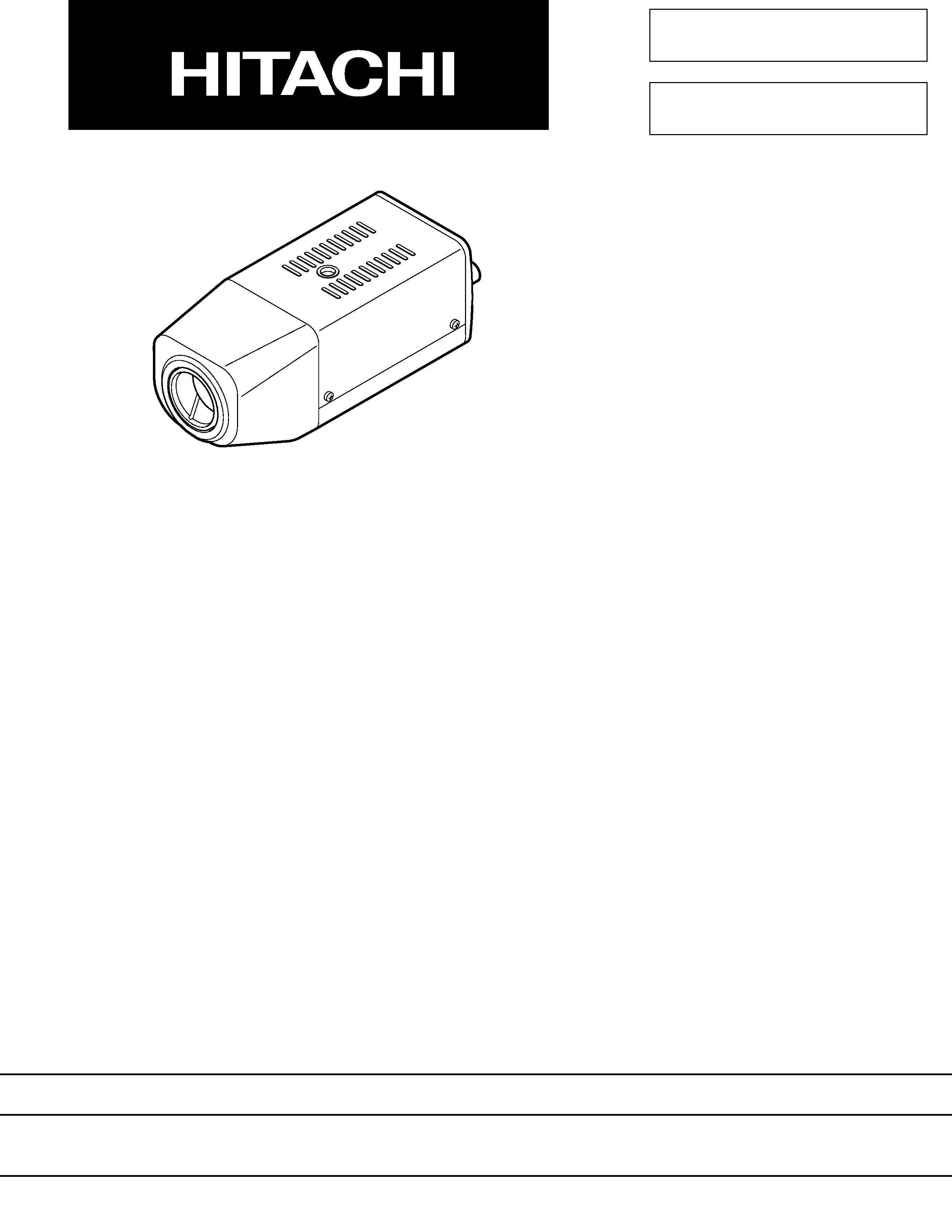
COLOR VIDEO CAMERA
2001
September
SM8105
VKC317E
Many electrical and mechanical parts have special safety-related characteristics. These are often not evident from visual
inspection nor can the protection afforded by them necessarily be obtained by using replacement components rated for a
higher voltage, wattage, etc. Replacement parts which have these special safety characteristics are identified in this
Service Manual. Electrical components having such features are identified by marking with a
on the schematics and
the parts list in this Service Manual. The use of a substitute replacement component which does not have the same
safety characteristics as the HITACHI recommended replacement one, shown in the parts list in this Service Manual, may
create shock, fire, or other hazards. Product safety is continuously under review and new instructions are issued from
time to time. For the latest information, always consult the current HITACHI Service Manual. A subscription to, or
additional copies for, HITACHI Service Manual may be obtained at a nominal charge from HITACHI SALES
CORPORATION.
PRODUCT SAFETY NOTICE
!
Cautions
Microsoft, MS, MS-DOS, Windows and Windows NT are registered trademarks of Microsoft Corporation.
Pentium and Celeron are registered trademarks of Intel Corporation.
Manufactured under license from Dolby Laboratories.
"Dolby" and double-D symbol are trademarks of Dolby Laboratories.
Confidential unpublished works. (C) 1992-1997 Dolby Laboratories Inc. All rights reserved.
IBM is registered trademarks of International Business Machines Corporations.
Other company names and product names listed are trademarks or brand names belonging to each company.
CHAPTER 1
GENERAL INFORMATION
1. Specifications ........................................................ 1-1
2. Comparison with Previous Model ......................... 1-2
2.1
Comparison of Specifications ........................ 1-2
2.2
Comparison of ICs ......................................... 1-2
3. Extract from the Instruction Manual ....................... 1-3
Controls and Functions ...................................... 1-3
Connection .......................................................... 1-4
CHAPTER 2
DISASSEMBLY
1. Procedure .............................................................. 2-1
CHAPTER 3
ELECTRIC CIRCUIT
ADJUSTMENT
1. Test Equipment/Jigs Necessary for Adjustment .. 3-1
1.1
List of Equipment and Jigs ............................. 3-1
1.2
List of Charts for Adjustment .......................... 3-1
1.3
Test Equipment, etc. ....................................... 3-1
2. Before Stating Adjustment ..................................... 3-2
2.1
Connections for Adjustment ........................... 3-2
2.2
Notes .............................................................. 3-2
2.3
Setting Video Camera .................................... 3-3
2.4
Setting Test Equipment .................................. 3-3
3. List of Adjustment Items ........................................ 3-3
4. Starting Adjustment Program (KMAP) ................... 3-4
5. Data Initilize Procedure ......................................... 3-5
5.1
Data Initilize ..................................................... 3-5
6. Electronic Volume Adjustment Procedure ............ 3-5
6.1
CDS Sampling Pulse Adjustment .................. 3-6
7. Camera Adjustment (Adjustment) Procedure ...... 3-6
7.1
Auto Iris Control Adjustment ........................... 3-6
7.2
White Balance Adjustment ............................. 3-7
7.3
Chroma Gain Adjustment ............................... 3-7
8. Error Messages ..................................................... 3-8
CHAPTER 4
EXPLODED VIEW
1. Exploded View ....................................................... 4-1
CHAPTER 5
REPLACEMENT
PARTS LIST
1. Mechanical Parts List ............................................ 5-1
2. Electrical Parts List ................................................ 5-1
CHAPTER 6
SCHEMATIC, CIRCUIT
BOARD AND BLOCK DIAGRAMS/
MICROPROCESSOR PIN FUNCTION
TABLES
Schematic Diagrams
Internal Wiring Diagram .............................................. 6-1
Waveforms .................................................................. 6-2
Sensor [S] .................................................................... 6-3
Process [PC] ............................................................... 6-6
Ext, Sync [EXT] ............................................................. 6-9
BNC Connector [BNC] ................................................. 6-11
Switch [SW] .................................................................. 6-12
Power [PWR] ............................................................... 6-13
AC Terminal [AC] ......................................................... 6-13
Circuit Board Diagrams
S -Side A/B- ................................................................. 6-15
PC -Side A/B- ............................................................... 6-17
EXT -Side A/B- ............................................................. 6-19
BNC -Side A/B- ............................................................ 6-20
SW -Side A/B- .............................................................. 6-21
PWR -Side A/B- ........................................................... 6-23
AC ............................................................................... 6-24
Identification of Parts Location
S
............................................................................... 6-15
PC ............................................................................... 6-17
EXT .............................................................................. 6-19
SW ............................................................................... 6-22
PWR ............................................................................ 6-23
Block Diagrams
Main ............................................................................. 6-25
Sub .............................................................................. 6-27
Microprocessor Pin Function Tables
Digital Microprocessor (IC1106: D-µP) ...................... 6-29
Contents
CONTENTS/CAUTION
Notes When Using Service Manual
The following shows the contents to be noted when using service manual:
1. Value units used in parts list
This table shows locations of each part on circuit board
diagrams. The locations are indicated using the guide
scales on the external lines of diagrams.
1) One diagram indicated for each board
The values, dielectric strength (power capacitance) and
tolerances of the resistors (excluding variable resistors)
and capacitors are indicated in the schematic diagrams
using abbreviations.
[Resistors]
Certain symbols are indicated below for value units of
resistors, capacitors and coils in parts list. When you
read them note the following regular indications:
Indication in list
Regular indication
KOHM ........................................... k
UF ................................................ µF
PF ................................................ pF
UH ................................................ µH
MH .............................................. mH
Parts
Resistor
Capacitor
Coil
2) Two diagrams indicated for each board
2. Values in schematic diagrams
Item
Value
Tolerance
Power
capacitance
Indication
No indication ..................................
K ................................................... k
M .................................................. M
No indication ............................ ±5%
(All tolerances other than ±5% are
indicated in schematic diagrams)
No indication ........................... 1/8W
(1/16W for leadless resistors without
indication)
All capacitances other than the above
are indicated in schematic diagrams.
[Capacitors]
Item
Value
Dielectric
strength
Indication
No indication ................................ µF
P ................................................... pF
No indication ............................. 50V
(All dielectric strengths other than 50V
are indicated in schematicdiagrams)
Item
Value
Indication
µ .................................................... µH
m ................................................. mH
[Coils]
3. Identifications of sides A/B in
circuit board diagrams
1) Board having a pattern on one side and parts on both
sides.
Side A:
Shows discrete parts, viewed from the
pattern
side.
Side B: Shows leadless parts, viewed from the
pattern side.
2) Board having patterns on both sides and parts on
both sides.
Side A:
Shows parts and patterns which can be
seen
when the case is opened.
Side B: Shows parts and the pattern on the back of
side A.
4. Table for indexing locations of parts
Parts
Location
2
A
Symbol
No.
IC
IC1201
Type of part
Zone "A" on board diagram
Circuit No.
Zone "2" on board diagram
Parts
Location
A - 2
A
Symbol
No.
IC
IC1201
Zone "2" on board
diagram
A: Shows side A
B: Shows side B
Zone "A" on board
diagram
Type of
part
Circuit No.
CAUTION

1 -
1
CHAPTER1
GENERALINFORMATION
1 .
Specifications
Signal
PAL
standard
625
TV
Lines,
50
fields
Image
sensor
1/4-inch
CCD
Image
sensor
Number
of
effective
pixels
752
(H)
×
582
(V)
Total number of pixels
795 (H) × 596 (V)
Scanning system
2 : 1 Interlaced
Scanning frequency
Horizontal
:
15.625 kHz
Vertical
:
50 Hz
Sync format
Internal/Line Lock
Video signal output
VBS
:
1.0Vp-p
Video
:
approx. 0.7 Vp-p positive
Sync
:
approx. 0.3 Vp-p negative
Burst
:
approx. 0.3 Vp-p 8 cycles or more
Impedance
:
75 ohm unbalanced
Connector
:
BNC
type
S/N ratio
50 dB or more
Horizontal resolution
450 TV Lines or more
Minimum required illumination
4 lx or less (F 1.2 wide angle AGC mode NORM)
2 lx or less (F 1.2 wide angle AGC mode HIGH)
White balance adjustment
Automatic or manual (switchable)
Adjustment range : 2,700 to 8,000 K
Lens
F 1.2 Optical zoom × 2.5. f: 2.4 mm to 6.0 mm
Permissible operating
Range in which operation is possible:
temperature/humidity
-10 to +50 °C / 10 to 85 %
Range in which performance is assured:
+5 to 30 °C / 45 to 75 %
Power input
AC 24 V ± 20 % (AC 19.2 V to AC 28.8 V) 50 Hz
DC 12 V (DC 10.8 V to DC 40 V)
Power consumption
3.0 W MAX
Dimensions
64 (W) × 58 (H) × 152 (D) mm (excluding protrusions)
Weight
370
g
1 -
2
ITEM
Signal
Image sensor
Number of effective pixels
Total number of pixels
Scanning system
Scanning frequency
Sync format
Video signal output
VBS
Video
Sync
Burst
Impedance
Connector
S/N ratio
Horizontal resolution
Minimum required illumination
White balance adjustment
Lens
Permissible operation
Power input
Power consumption
Dimensions
Weight
2 . 2 Comparison of ICs
ITEM
CCD Image Sensor
DrivePulse
Gen.
Iris
Drive
CDS AGC & A/D Conv.
Digital
Process
(DSP)
Digital
µP
EEPROM
Reset
Pulse
Gen.
Character
Gen.
Inverter
(INV)
Pulse
Gen.
Phase
Det.
Pulse
Switch
Inverter
(INV)
V.Pulse
Shape
PWM
Video
Amp
Photo-coupler
Switch
2 . 1 Comparison of Specifications
2 .
Comparison with Previous Model
ICX209AK-6 (IC1001)
µPD16510GR
(IC1002)
NJM2904
(IC1041)
HD49322BF
(IC1102)
HG73C012TE
(IC1103)
HD6433042ST50F
(IC1106)
S29394AFJA
(IC1107)
RN5VT28AA-TL
(IC1108)
µPD6466GS
(IC1111)
TC7SU04F
(IC1112)
TC7SU04F
(IC1113)
TC7SU04F
(IC1116)
µPD74HC00G
(IC1115)
74VHC4046MTCX
(IC1202)
µPD4066BG
(IC1203)
NJU74HC04M
(IC1204)
µPD74HC221AG
(IC1207)
TL1464IPT
(IC1501)
MM1029AF
(IC1601)
HA17431PA
(IC3501)
PAL
Standard
625
TV
lines,
50
fields
1/4-inch
CCD
image
sensor
752
(H)
×
582
(V)
795
(H)
×
596
(V)
2
:
1
Interlaced
Horizontal:
15.625
kHz
Vertical: 50 Hz
Internal/Line
Lock
1.0
Vp-p
approx.
0.7
Vp-p
positive
approx.
0.3
Vp-p
negative
approx.
0.3
Vp-p
8
cycles
or
more
75
ohm
unbalanced
BNC
type
50 dB or more
450 TV line or more
4 lx or less
(F 1.2 wide angle AGC mode NORM)
2 lx or less
(F 1.2 wide angle AGC mode HIGH)
Automatic or manual (switchable)
Adjustment
range
:
2,700
to
8,000
K
F 1.2 Optical zoom × 2.5. f: 2.4 mm to 6.0mm
Range in which operation is possible:
-10 to +50 °C / 10 to 85 %
Range in which performance is assured:
+5 to 30 °C / 45 to 75 %
AC 24 V ± 20% (AC 19.2 V to AC 28.8 V) 50 Hz
DC 12 V (DC 10.8 V to DC 40 V)
3.0 W MAX
64 (W) × 58 (H) × 152 (D) mm (excluding protrusions)
370 g
VK-C317E
VK-C317E
VK-C307E
1/4-inch
CCD
image
sensor
500
(H)
×
582
(V)
537
(H)
×
597
(V)
330 TV lines or more
2 lx or less
(F 1.2 wide angle AGC mode NORM)
1 lx or less
(F 1.2 wide angle AGC mode HIGH)
VK-C307E
ICX207AK-6(IC1001)