SERVICE MANUAL
SERVICE MANUAL
SERVICE MANUAL
SERVICE MANUAL
SERVICE MANUAL
SPECIFICATIONS AND PARTS ARE SUBJECT TO CHANGE FOR IMPROVEMENT
Digital Media Products Division
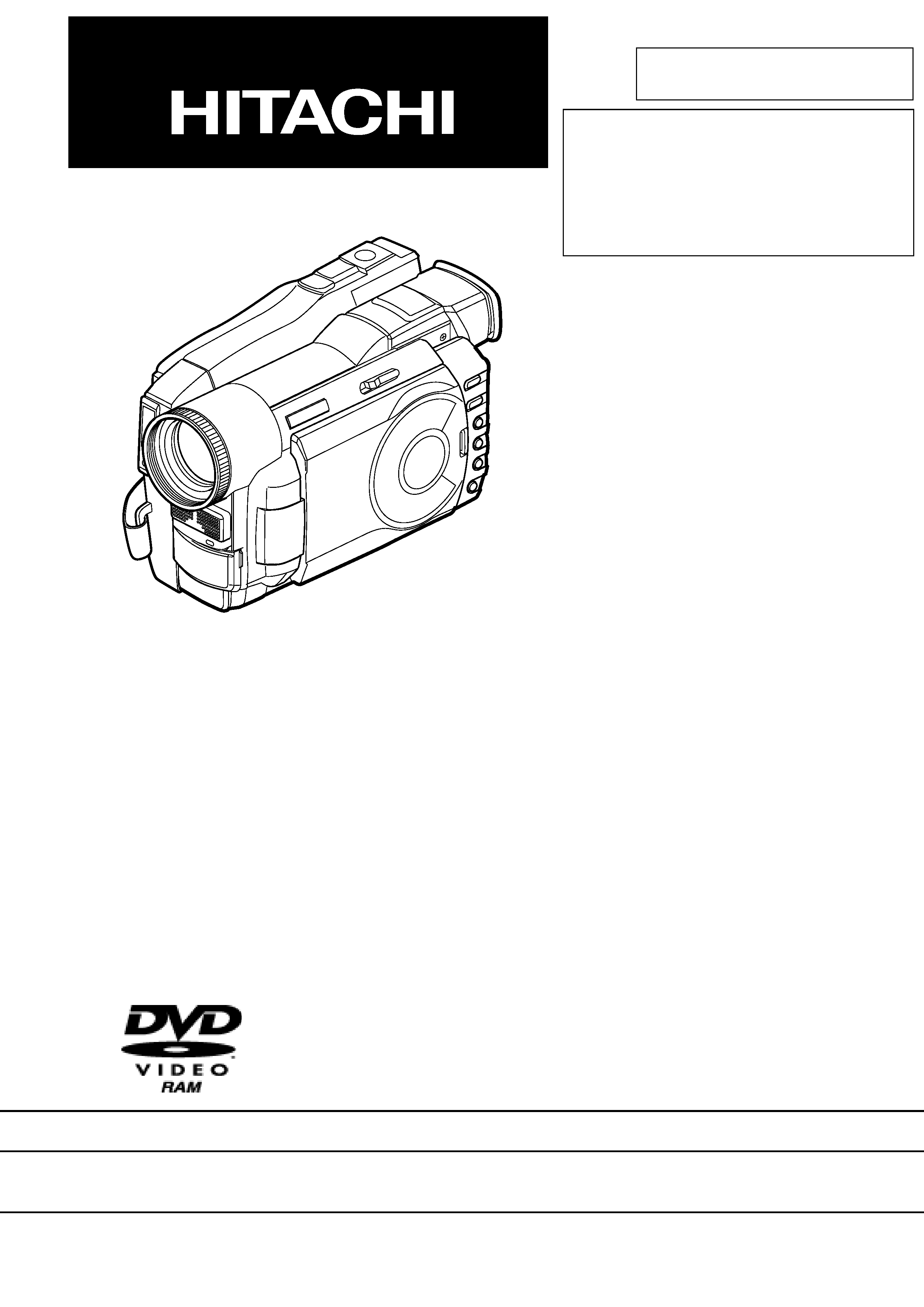
DVD VIDEO CAMERA/RECORDER
2001
March
SM7108
DZMV100E
DZMV100EAU
DZMV100EUK
Microsoft, MS, MS-DOS, Windows and Windows NT are registered trademarks of Microsoft Corporation.
Pentium and Celeron are registered trademarks of Intel Corporation.
Manufactured under license from Dolby Laboratories.
"Dolby" and double-D symbol are trademarks of Dolby Laboratories.
Confidential unpublished works. (C) 1992-2000 Dolby Laboratories Inc. All rights reserved.
IBM is registered trademarks of International Business Machines Corporations.
Other company names and product names listed are trademarks or brand names belonging to each company.
CAUTION-1
CAUTION (COLOR LCD)
CAUTION (COLOR LCD)
CAUTION (COLOR LCD)
CAUTION (COLOR LCD)
CAUTION (COLOR LCD)
LCD display; the liquid crystal display (LCD) panel is made by highly precise technology.
More than 99.99% of its picture elements (pixels) are effective, but some (less than 0.01%) may appear as colored
bright dots. This does not indicate a fault as the LCD panel stretches the limits of current technology.
CLASS 1
LASER PROCTECT
CAUTION
This product contains a laser diode of
higher class than 1. To ensure contin-
ued safety, do not remove any covers
or attempt to gain access to the in-
side of the product. Refer all servicing
to qualified personnel.
CAUTION
BLE
VISI
AND INVISIBLE
LASER RADIATION WHEN OPEN.
AVOID EXPOSURE TO BEAM.
Contents included:
Contents included:
Contents included:
Contents included:
Contents included:
ANA and DIG circuit board diagrams included are for reference during troubleshooting.
This manual does not include the schematic diagrams of ANA and DIG circuit boards, since these boards must be
replaced in units of board and their components are not assigned as service parts.
SHD, RAM2LD and PHD circuit board diagrams included are for reference during troubleshooting.
This manual does not include the schematic diagrams of SHD, RAM2LD and PHD circuit boards, since these
boards are included in the mechanism unit and they or their components are not assigned as service parts.
Many electrical and mechanical parts have special safety-related characteristics. These are often not evident from visual
inspection nor can the protection afforded by them necessarily be obtained by using replacement components rated for a
higher voltage, wattage, etc. Replacement parts which have these special safety characteristics are identified in this
Service Manual. Electrical components having such features are identified by marking with a
on the schematics and
the parts list in this Service Manual. The use of a substitute replacement component which does not have the same safety
characteristics as the HITACHI recommended replacement one, shown in the parts list in this Service Manual, may create
shock, fire, or other hazards. Product safety is continuously under review and new instructions are issued from time to time.
For the latest information, always consult the current HITACHI Service Manual. A subscription to, or additional copies for,
HITACHI Service Manual may be obtained at a nominal charge from HITACHI SALES CORPORATION.
PRODUCT SAFETY NOTICE
PRODUCT SAFETY NOTICE
PRODUCT SAFETY NOTICE
PRODUCT SAFETY NOTICE
PRODUCT SAFETY NOTICE
!
Lithium battery; danger of explosion if battery is incorrectly replaced. Replace only with the same or equivalent type
recommended by the equipment manufacturer. Discard used batteries according to manufacuturer's instructions.
When replacing the lithium battery it is important to use the same type and connect it correctly.
WARNING:
Lithium batteries contain dangerous chemicals.
Handle and dispose of with great care.
Do not throw in a fire.
Do not short circuit it.
For disposal place in a plastic bag and put in waste bin.
CAUTION
CAUTION
CAUTION
CAUTION
CAUTION
CAUTION-2
Notes When Using Service Manual
Notes When Using Service Manual
Notes When Using Service Manual
Notes When Using Service Manual
Notes When Using Service Manual
The following shows the contents to be noted when using service manual:
The following shows the contents to be noted when using service manual:
The following shows the contents to be noted when using service manual:
The following shows the contents to be noted when using service manual:
The following shows the contents to be noted when using service manual:
1. Value units used in parts list
1. Value units used in parts list
1. Value units used in parts list
1. Value units used in parts list
1. Value units used in parts list
This table shows locations of each part on circuit board
diagrams. The locations are indicated using the guide
scales on the external lines of diagrams.
1) One diagram indicated for each board
The values, dielectric strength (power capacitance) and
tolerances of the resistors (excluding variable resistors)
and capacitors are indicated in the schematic diagrams
using abbreviations.
[Resistors]
[Resistors]
[Resistors]
[Resistors]
[Resistors]
Certain symbols are indicated below for value units of
resistors, capacitors and coils in parts list. When you read
them note the following regular indications:
Indication in list
Regular indication
KOHM ........................................... k
UF ................................................ µF
PF ................................................ pF
UH ................................................ µH
MH ............................................... mH
Parts
Resistor
Capacitor
Coil
2) Two diagrams indicated for each board
2. Values in schematic diagrams
2. Values in schematic diagrams
2. Values in schematic diagrams
2. Values in schematic diagrams
2. Values in schematic diagrams
Item
Value
Tolerance
Power
capacitance
Indication
No indication ...................................
K
................................................ k
M
............................................... M
No indication ............................. ±5%
(All tolerances other than ±5% are
indicated in schematic diagrams)
No indication ............................ 1/8W
(1/16W for leadless resistors without
indication)
All capacitances other than the above
are indicated in schematic diagrams.
[Capacitors]
[Capacitors]
[Capacitors]
[Capacitors]
[Capacitors]
Item
Value
Dielectric
strength
Indication
No indication ................................. µF
P
................................................ pF
No indication .............................. 50V
(All dielectric strengths other than 50V
are indicated in schematic diagrams)
Item
Value
Indication
µ
................................................ µH
m
............................................... mH
[Coils]
[Coils]
[Coils]
[Coils]
[Coils]
3. Identifications of sides A/B in
3. Identifications of sides A/B in
3. Identifications of sides A/B in
3. Identifications of sides A/B in
3. Identifications of sides A/B in
circuit board diagrams
circuit board diagrams
circuit board diagrams
circuit board diagrams
circuit board diagrams
1) Board having a pattern on one side and parts on both
sides.
Side A: Shows discrete parts, viewed from the pattern
side.
Side B: Shows leadless parts, viewed from the
pattern side.
2) Board having patterns on both sides and parts on
both sides.
Side A: Shows parts and patterns which can be seen
when the case is opened.
Side B: Shows parts and the pattern on the back of
side A.
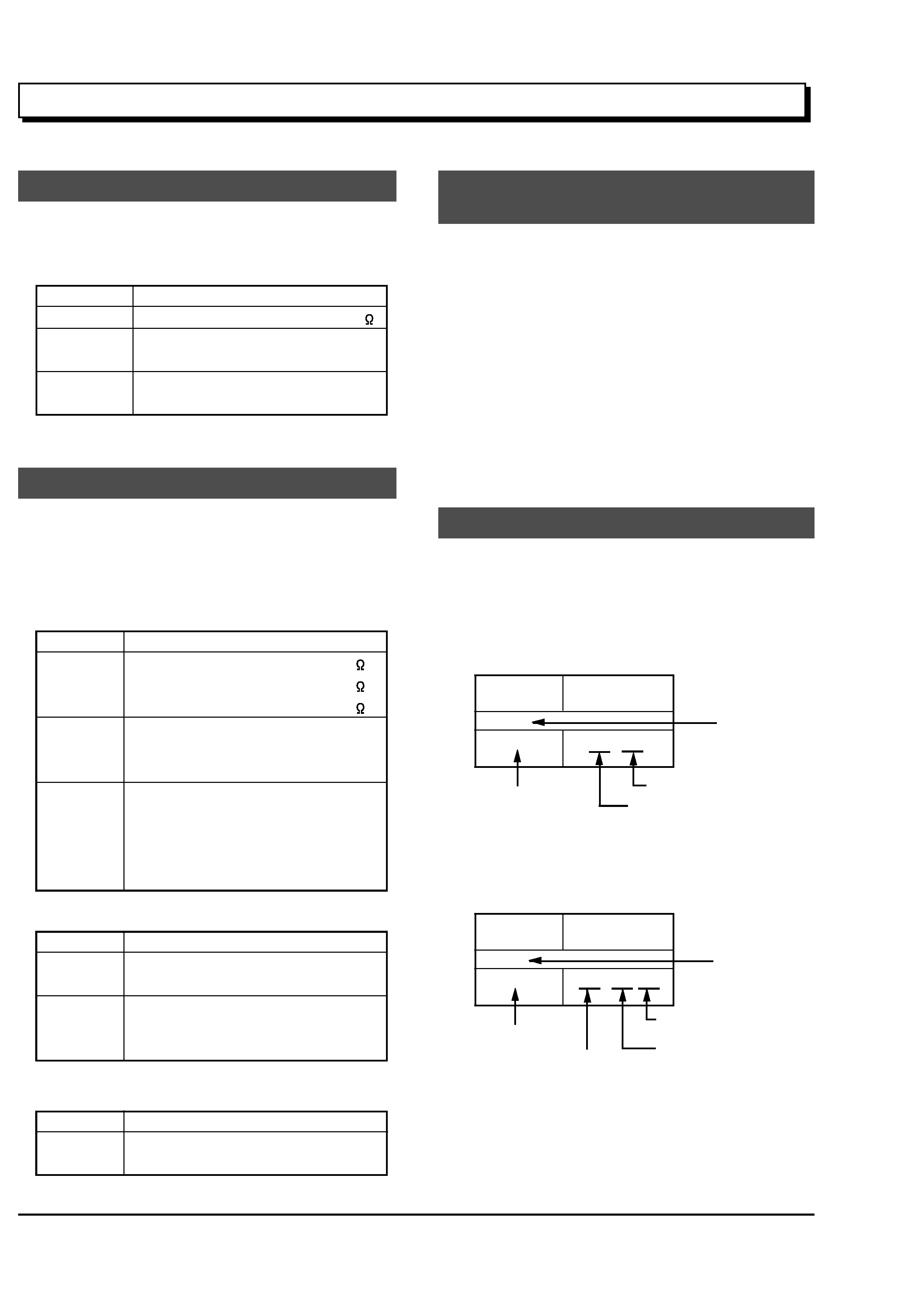
4. Table for indexing locations of parts
4. Table for indexing locations of parts
4. Table for indexing locations of parts
4. Table for indexing locations of parts
4. Table for indexing locations of parts
Parts
Location
2
A
Symbol
No.
IC
IC1201
Type of part
Zone "A" on board diagram
Circuit No.
Zone "2" on board diagram
Parts
Location
A - 2
A
Symbol
No.
IC
IC1201
Zone "2" on board
diagram
A: Shows side A
B: Shows side B
Zone "A" on board
diagram
Type of
part
Circuit No.

CONTENTS-1
CHAPTER 1
CHAPTER 1
CHAPTER 1
CHAPTER 1
CHAPTER 1
GENERAL INFORMA
GENERAL INFORMA
GENERAL INFORMA
GENERAL INFORMA
GENERAL INFORMATION
TION
TION
TION
TION
1. Specifications ...................................................... E1-1
2. Information on DVD-RAM Discs ......................... E1-2
2.1
Comparison of DVD-RAM Discs .................. E1-2
2.2
DVD Video Recording Standard ................. E1-2
2.3
Comparison between
DVD-RAM and DVD-RW/R .......................... E1-3
2.4
Available DVD-RAM Discs ........................... E1-3
2.5
Initializing (formatting) DVD-RAM Discs ...... E1-4
2.6
Handling DVD-RAM Disc ............................. E1-4
2.7
Removing DVD-RAM Disc from Cartridge ... E1-4
3. Subsidiary Functions for Servicing ..................... E1-6
3.1
Forced disc formatting .................................. E1-6
3.2
Still (JPEG) file operation ............................. E1-6
3.3
Firmware version display ............................. E1-7
3.4
Error code display ........................................ E1-7
3.5
Playback file detailed information display .... E1-8
3.6
Deleting information control (RX) file ........... E1-8
4. Explanation of Trouble Messages ...................... E1-9
5. Troubleshooting Guide of DVD Video
Camera/recorder ................................................. E1-13
6. Updating Firmware .............................................. E1-16
6.1
Firmware programs ...................................... E1-16
6.2
How to update .............................................. E1-16
7. Service Manual Abbreviation List ....................... E1-17
8. Fro the Battery .................................................... E1-19
9. Extract from the Instruction Manual .................... E1-20
Cleaning ....................................................... E1-20
Names of Parts ............................................ E1-20
System Reset ............................................... E1-22
Setting Up the Battery .................................. E1-23
Setting Date and Time ................................. E1-24
Initializing DVD-RAM Disc ............................ E1-25
Trouble Messages ........................................ E1-26
CHAPTER 2
CHAPTER 2
CHAPTER 2
CHAPTER 2
CHAPTER 2
DISASSEMBL
DISASSEMBL
DISASSEMBL
DISASSEMBL
DISASSEMBLY
Y
Y
Y
Y
1. Parts Location ..................................................... E2-1
2. Before Starting Disassembly .............................. E2-3
3. Disassembly Procedure ...................................... E2-5
3.1
Top Cover, R-Block, L-Block ........................ E2-5
3.2
LCD-U Case, LCD Block, Front Block,
RUB Sheet ................................................... E2-6
3.3
Jack Cover, Flash Unit, JKR Circuit Board,
JKF Circuit Board, Microphone, IR Filter,
Lens Hood, Front Case ................................ E2-8
3.4
EVF Block, Rear Cover, Power Terminal ..... E2-9
3.5
ANA Circuit Board, Camera Block, DIG
Circuit Board, LSP Shield, Side Case-L ....... E2-10
3.6
Disc Cover, Switch Unit ................................ E2-10
3.7
Link Bracket R, Link Bracket L, Loader,
Mechanism Unit ........................................... E2-12
3.8
Lock Unit, Side Case-R ................................ E2-14
3.9
GYR Circuit Board, SEN Circuit Board,
Sensor, Lens ................................................ E2-14
CONTENTS
CONTENTS
CONTENTS
CONTENTS
CONTENTS
3.10 Eye Control, EVF-F Case, Plate-F,
EVF-B Case, EVF LCD, EVF Backlight,
EBL Circuit Board ......................................... E2-16
3.11 B/W LCD, LCD Power Unit, LCD Frame,
Backlight, Color LCD, LCD-B Case ............. E2-17
4. Disassembly When Trouble Has Occurred ......... E2-18
4.1
Cleaning EVF Screen
(Removing Eye Control) ............................... E2-18
4.2
Removing DVD-RAM Disc ........................... E2-18
5. Information on Installation Position of
Shields, etc. ........................................................ E2-21
5.1
Side Case-L ................................................. E2-21
5.2
DIG Circuit Board ......................................... E2-21
5.3
ANA Circuit Board ........................................ E2-22
5.4
Power Terminal ............................................ E2-22
5.5
Front Block ................................................... E2-22
5.6
Mechanism Unit ........................................... E2-23
5.7
Miscellaneous .............................................. E2-24
CHAPTER 3
CHAPTER 3
CHAPTER 3
CHAPTER 3
CHAPTER 3
ELECTRIC CIRCUIT
ELECTRIC CIRCUIT
ELECTRIC CIRCUIT
ELECTRIC CIRCUIT
ELECTRIC CIRCUIT
ADJUSTMENT
ADJUSTMENT
ADJUSTMENT
ADJUSTMENT
ADJUSTMENT
1. Test Equipment/Jigs Necessary for
Adjustment ......................................................... E3-1
1.1
List of equipment and jigs ............................ E3-1
1.2
List of charts for adjustment ......................... E3-1
1.3
Test equipment, etc. ..................................... E3-1
2. Before Starting Adjustment ................................. E3-2
2.1
Connection for adjustment ........................... E3-2
2.2
Notes ............................................................ E3-2
2.3
Setting video camera/recorder ..................... E3-2
2.4
Setting test equipment ................................. E3-3
3. List of Adjustment Item ...................................... E3-4
4. Starting Adjustment Program (MAP: Manual
Adjustment Program) .......................................... E3-5
5. Adjustment Procedure ........................................ E3-6
5.1
Data Initialize ................................................ E3-6
(1) Data Initialize ................................................ E3-6
5.2
Adjustment ................................................... E3-6
(1) Sampling Pulse Adjustment ......................... E3-7
(2) Auto Iris Control Adjustment ........................ E3-7
(3) Shutter Adjustment ....................................... E3-8
(4) White Balance Adjustment ........................... E3-10
(5) Chroma Gain Adjustment ............................. E3-10
5.3
Autofocus ..................................................... E3-12
(1) Zoom/Focus Tracking Adjustment ............... E3-12
(2) AF Noise Level Adjustment .......................... E3-12
5.4
Stabilizer ...................................................... E3-13
(1) Stabilizer Adjustment ................................... E3-13
5.5
Spot Noise .................................................... E3-13
(1) Spot Noise Adjustment ................................. E3-13
6. Error Message .................................................... E3-15
6.1
Error Message of Adjustment ....................... E3-15
6.2
Error Message of Autofocus ........................ E3-16
6.3
Error Message of Stabilize ........................... E3-16
6.4
Error Message of Spot Noise ....................... E3-16

CONTENTS-2
CHAPTER 4
CHAPTER 4
CHAPTER 4
CHAPTER 4
CHAPTER 4
EXPLODED
EXPLODED
EXPLODED
EXPLODED
EXPLODED VIEW
VIEW
VIEW
VIEW
VIEW
CABINET-1 ............................................................... 4-1
CABINET-2 ............................................................... 4-2
ELECTRONIC VIEWFINDER (EVF) ......................... 4-3
LCD ........................................................................... 4-3
CAMERA .................................................................. 4-4
ACCESSORIES ........................................................ 4-4
CHAPTER 5
CHAPTER 5
CHAPTER 5
CHAPTER 5
CHAPTER 5
REPLA
REPLA
REPLA
REPLA
REPLACEMENT
CEMENT
CEMENT
CEMENT
CEMENT
P
P
P
P
PAR
AR
AR
AR
ARTS LIST
TS LIST
TS LIST
TS LIST
TS LIST
1. MECHANICAL PARTS LIST ............................... 5-1
2. ELECTRICAL PARTS LIST ................................ 5-2
CHAPTER 6
CHAPTER 6
CHAPTER 6
CHAPTER 6
CHAPTER 6
SCHEMA
SCHEMA
SCHEMA
SCHEMA
SCHEMATIC,
TIC,
TIC,
TIC,
TIC, CIRCUIT BO
CIRCUIT BO
CIRCUIT BO
CIRCUIT BO
CIRCUIT BOARD
ARD
ARD
ARD
ARD
AND BLOCK DIA
AND BLOCK DIA
AND BLOCK DIA
AND BLOCK DIA
AND BLOCK DIAGRAMS
GRAMS
GRAMS
GRAMS
GRAMS
SCHEMATIC DIAGRAMS
INTERNAL WIRING DIAGRAM ............................ 6-1
SENSOR [SEN] ..................................................... 6-3
GYRO [GYR] ......................................................... 6-4
EVF BACK LIGHT [EBL] ....................................... 6-5
JACK-F [JKF] ........................................................ 6-6
JACK-R [JKR] ........................................................ 6-7
CIRCUIT BOARD DIAGRAMS
SEN ....................................................................... 6-9
GYR ....................................................................... 6-9
EBL ........................................................................ 6-10
ANA [SIDE-A] (*1) ................................................. 6-11
ANA [SIDE-B] (*1) ................................................. 6-13
DIG [SIDE-A] (*1) .................................................. 6-15
DIG [SIDE-B] (*1) .................................................. 6-17
JKF ........................................................................ 6-19
JKR ........................................................................ 6-19
SHD (*2) ................................................................ 6-20
RAM2LD (*2) ......................................................... 6-20
PHD (*2) ................................................................ 6-21
BLOCK DIAGRAMS
AV PROCESS SECTION ...................................... 6-23
8cm DVD-RAM DRIVE SECTION ......................... 6-25
*1: The circuit board diagrams included are for reference
during troubleshooting.
This manual does not include the schematic diagrams
of ANA and DIG circuit boards, since these boards
must be replaced in units of board and their
components are not assigned as service parts.
*2: The circuit board diagrams included are for reference
during troubleshooting.
This manual does not include the schematic diagrams
of SHD, RAM2LD and PHD circuit boards, since these
boards are included in the mechanism unit and they or
their components are not assigned as service parts.