
CAUTION:
Before servicing this chassis, it is important that the service technician read the "Safety
Precautions" and "Product Safety Notices" in this service manual.
ATTENTION:
Avant d'effectuer l'entretien du châassis, le technicien doit lire les «Précautions de sécurité»
et les «Notices de sécurité du produit» présentés dans le présent manuel.
VORSICHT:
Vor Öffnen des Gehäuses hat der Service-Ingenieur die ,,Sicherheitshinweise" und ,,Hinweise
zur Produktsicherheit" in diesem Wartungshandbuch zu lesen.
SERVICE MANUAL
MANUEL D'ENTRETIEN
WARTUNGSHANDBUCH
Data
contained
within
this
Service
manual is subject to alteration for
improvement.
Les données fournies dans le présent
manuel d'entretien peuvent faire l'objet
de modifications en vue de perfectionner
le produit.
Die
in
diesem
Wartungshandbuch
enthaltenen Spezifikationen können sich
zwecks Verbesserungen ändern.
SPECIFICATIONS AND PARTS ARE SUBJECT TO CHANGE FOR IMPROVEMENT
Colour Television
August 2003
No. 0112
C2844S
CL2843S
CP2843S
C32W460N
CG32W460N

1
CONTENTS
SAFETY PRECAUTIONS: ................................................................................................................................... 2
TV set switched off .......................................................................................................................................... 2
Measurements ................................................................................................................................................ 2
PERI-TV SOCKET ............................................................................................................................................... 2
SCART 1 2
SCART 2 2
1. INTRODUCTION ............................................................................................................................................. 2
2.SMALL SIGNAL PART WITH STV2248 ........................................................................................................... 3
2.1 Vision IF amplifier................................................................................................................................... 3
2.2 QSS Sound circuit (QSS versions) ......................................................................................................... 3
2.3 FM demodulator and audio amplifier (mono versions) ......................................................................... 3
2.4 Video switch ............................................................................................................................................ 3
2.5 Synchronisation circuit ............................................................................................................................ 3
2.6 Chroma and luminance processing ...................................................................................................... 4
2.7 RGB output circuit ................................................................................................................................... 4
2.8 µ-Controller ............................................................................................................................................. 4
3. TUNER ............................................................................................................................................................ 5
4- MULTISTANDARD SOUND PROCESSOR .................................................................................................... 5
5. SOUND OUTPUT STAGE TDA7269A ............................................................................................................. 5
6. VERTICAL OUTPUT STAGE WITH STV9306 ............................................................................................. 5-6
7. VIDEO OUTPUTAMPLIFIER STV5112 ........................................................................................................... 6
8. POWER SUPPLY (SMPS) ............................................................................................................................... 6
9. POWER FACTOR CORRECTION .................................................................................................................. 6
10. SERIAL ACCESS CMOS 8K EEPROM 24C08 ............................................................................................. 6
11. CLASS AB STEREO HEADPHONE DRIVER TDA1308 ................................................................................ 6
12. CLASS AB MONO SUBWOOFER DRIVER TDA7261 ................................................................................... 6
13. SAW FILTERS ............................................................................................................................................... 6
14. IC DESCRIPTIONS AND INTERNAL BLOCK DIAGRAM .............................................................................. 6
ST92195 ....................................................................................................................................................... 7
STV224X ................................................................................................................................................... 7-8
UV1315, UV1316, UV1336 ...................................................................................................................... 8-9
TDA7269A .................................................................................................................................................. 10
STV9306 ..................................................................................................................................................... 10
STV5112 ..................................................................................................................................................... 11
MC44608 .................................................................................................................................................... 11
MSP 34XXG ................................................................................................................................................ 12
24C08 ................................................................................................................................................... 12-13
TDA1308 .................................................................................................................................................... 13
TDA7261 .................................................................................................................................................... 13
SAW FILTERS ............................................................................................................................................. 14
15.CIRCUIT DESCCIRIPTION ................................................................................................................... 15-19
16.CHASSIS MANUALADJUSTMENT PROCEDURE ......................................................................20-22
17.OPTION SETTING ................................................................................................................................. 23-25
18.TUNER SETTING ........................................................................................................................................ 26
19.GENERAL BLOCK DIAGRAM of CHASSIS ....................................................................................27
20.TITANIUM - Languages Groups .......................................................................................................28
21.Features .............................................................................................................................................29
21.1 BLOCK DIAGRAM ................................................................................................................................. 30
21.2 SMPS BLOCK DIAGRAM ....................................................................................................................... 31
21.3 MICRO CONTROLLER BLOCK DIAGRAM ........................................................................................... 32
21.4 VIDEO BLOCK DIAGRAM ...................................................................................................................... 33
21.5 STEREO BLOCK DIAGRAM .................................................................................................................. 34
21.6 SCART BLOCK DIAGRAM ..................................................................................................................... 35
21.7 DEFLECTIOAN BLOCK DIAGRAM ........................................................................................................ 36
21.8 BASE BOADR BLOCK DIAGRAM .......................................................................................................... 37
22. CIRCUIT DIAGRAMS .................................................................................................................................. 38
22.1 SMPS CIRCUIT DIAGRAM .................................................................................................................... 38
22.2 MICRO CONTROLLER CIRCUIT DIAGRAM ......................................................................................... 39
22.3 VIDEO CIRCUIT DIAGRAM ................................................................................................................... 40
22.4 STEREO CIRCUIT DIAGRAM ............................................................................................................... 41
22.5 SCART CIRCUIT DIAGRAM .................................................................................................................. 42
22.6 BASE BOARD CIRCUIT DIAGRAM ....................................................................................................... 43
22.7 CRT BOARD CIRCUIT DIAGRAM ......................................................................................................... 44
2
DO NOT CHANGE ANY MODULE UNLESS THE SET IS SWITCH OFF
The mains supply side of the switch mode power supply transformer is live.
Use an isolating transformer.
The receivers fulfill completely the safety requirements.
Safety precautions:
Servicing of this TV should only be carried out by a qualified person. Components marked with the warning symbol
on the circuit diagram are critical for safety and must only be replaced with an identical component.
- Power resistor and fusable resistors must be mounted in an identical manner to the original component.
TV Set switched off:
Make short-circuit between HV-CRT clip and CRT ground layer.
Short C809 before changing IC800 end IC801 or other components in primary side of SMPS part.
Measurements:
Voltage readings and oscilloscope traces are measured under following conditions.
Antenna signals level is 60dB at the color bar pattern from the TV pattern generator.(100% white,75% colour saturation)
Brightness, contrast, and color are adjusted for normal picture perfomance.
Mains supply, 220VAC, 50Hz.
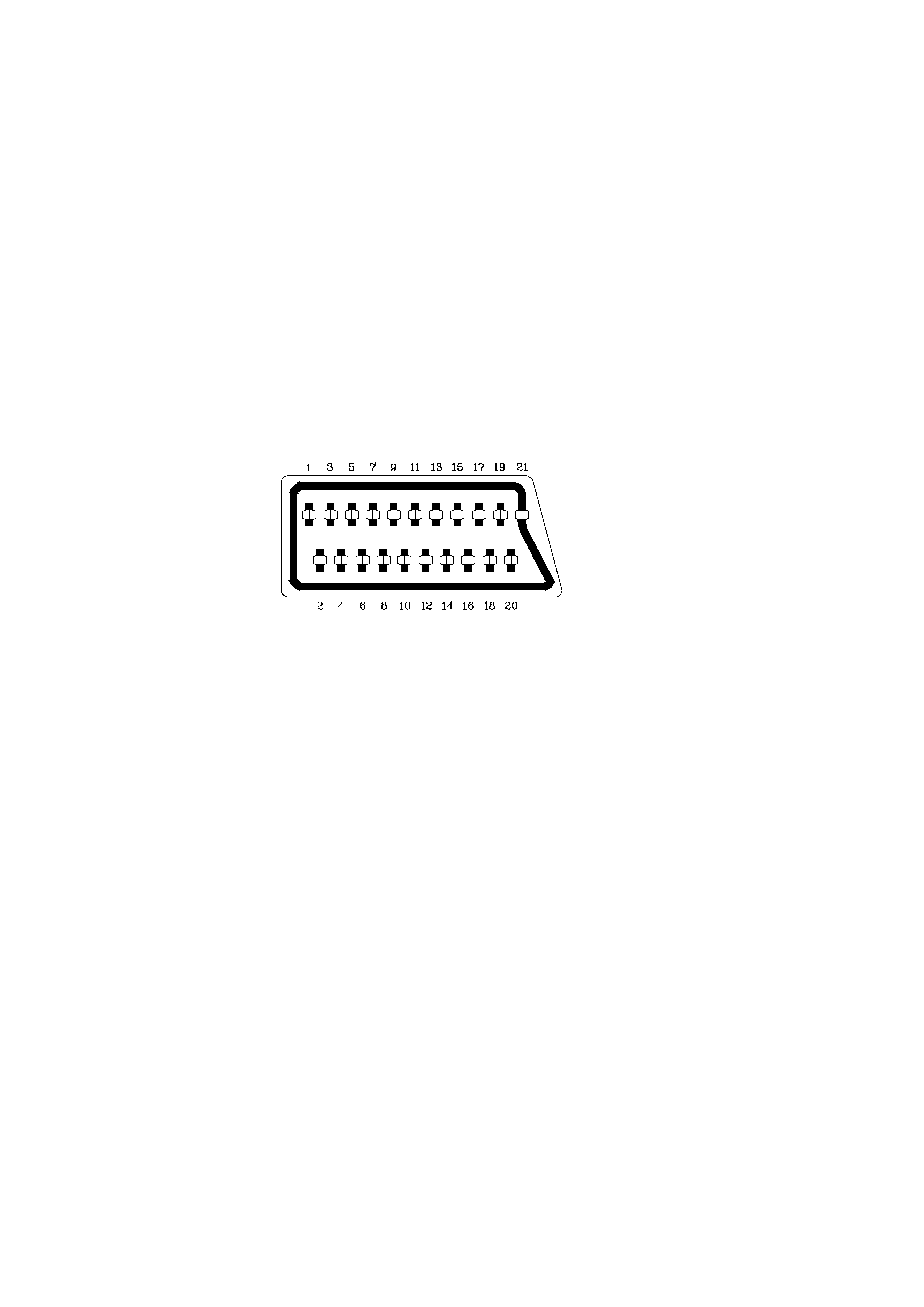
PERI-TV SOCKET
SCART 1 PINING
SCART 2 PINING
1
Audio right output 0.5Vrms / 1K
1 Audio right output
0.5Vrms / 1K
2
Audio right input
0.5Vrms / 10K
2 Audio right input
0.5Vrms / 10K
3
Audio left output
0.5Vrms / 1K
3 Audio left output
0.5Vrms / 1K
4
GroundAF
4 Ground AF
5
Ground Blue
5 Ground Blue
6
Audio left input
0.5Vrms / 10K
6 Audio left input
0.5Vrms / 10K
7
Blue input
0.7Vpp / 75ohm
7 Blue input
8
AV switching input 0-12VDC /10K
8 AV switching input
0-12VDC /10K
9
Ground Green
9 Ground Green
10 -
10 -
11 Green input
0.7Vpp / 75ohm
11 -
12 -
12 -
13 Ground Red
13 Ground Red
14 Ground Blanking
14 Ground Blanking
15 Red input
0.7Vpp / 75ohm
15 -
16 Blanking input
0-0.4VDC, 1-3VDC / 75ohm
16 -
17 Ground CVBS output
17 Ground CVBS output
18 Ground CVBS input
18 Ground CVBS input
19 CVBS output
1Vpp / 75ohm
19 CVBS output
1Vpp / 75ohm
20 CVBS input
1Vpp / 75ohm
20 CVBS input
1Vpp / 75ohm
21 Ground
21 Ground
1. INTRODUCTION
Th
is a 110° chassis capable of driving 25, 28, 29, 33 4:3 and 28, 32 16:9 tubes at the appropriate currents.
The chassis is capable of operating in PAL, SECAM and NTSC standards and multiple transmission standards as B/G,
D/K, I/I, and L/L´. standards. The sound system is capable of giving 12 watts RMS output into a load of 8 ohms.
One page, 7 page SIMPLETEXT, TOPTEXT, FASTTEXT and US Closed Caption is also provided. The chassis is
equipped with a double-deck 42 pin scart connector for AV input/output, front-AV input, one back-AV output, one SVHS,
one headphone and one subwoofer.

3
2. SMALL SIGNAL PART WITH STV2248:
STV2248 video processor is essential for realizing all small signal functions for a color TV receiver.
2.1 Vision IF amplifier
The vision IF amplifier can demodulate signals with positive and negative modulation. The PLL demodulator is
completely alignment-free. Although the VCO (Toko-coil) of the PLL circuit is external, yet the frequency is fixed to the
required value by the original manufacturer thus the Toko-coil does not need to be adjusted manually. The setting of the
various frequencies (38.9 or 45.75 MHz) can be made via changing the coil itself
2.2 QSS Sound circuit (QSS versions)
The sound IF amplifier is similar to the vision IF amplifier and has an external AGC de-coupling capacitor. The single
reference QSS mixer is realised by a multiplier. In this multiplier the SIF signal is converted to the inter-carrier frequency
by mixing it with the regenerated picture carrier from the VCO. The mixer output signal is supplied to the output via a
high-pass filter for attenuation of the residual video signals. With this system a high performance hi-fi stereo sound
processing can be achieved. The AM sound demodulator is realised by a multiplier. The modulated sound IF signal is
multiplied in phase with the limited SIF signal. The demodulator output signal is supplied to the output via a low-pass
filter for attenuation of the carrier harmonics. The AM signal is supplied to the output via the volume control.
The AM demodulated signal results from multiplying the input signal by itself, it is available on AM/FM output.
2.3 FM demodulator and audio amplifier (mono versions):
The FM demodulator is realized as narrow-band PLL with external loop filter, which provides the necessary selectivity
without using an external band-pass filter. To obtain a good selectivity a linear phase detector and constant input signal
amplitude are required. For this reason the inter-carrier signal is internally supplied to the demodulator via a gain
controlled amplifier and AGC circuit. The nominal frequency of the demodulator is tuned to the required frequency
(4.5/5.5/6.0/6.5 MHz) by means of a calibration circuit that uses the clock frequency of the µ-controller/Teletext decoder
as a reference. The setting to the wanted frequency is realized by means of the software. It can be read whether the PLL
frequency is inside or outside the window and whether the PLL is in lock or not. With this information it is possible to
make an automatic search system for the incoming sound frequency. This is realized by means of a software loop that
alternate the demodulator to various frequencies, then select the frequency on which a lock condition has been found.
De-emphasis output signal amplitude is independent of the TV standard and has the same value for a frequency deviation
of ±25 kHz at the 4.5 MHz standard and for a deviation of ±50 kHz for the other standards. When the IF circuit is
switched to positive modulation the internal signal on de-emphasis pin is automatically muted. The audio control circuit
contains an audio switch and volume control. In the mono inter-carrier sound versions the Automatic Volume Leveling
(AVL) function can be activated. The pin to which the external capacitor has to be connected depends on the IC version.
2.4 Video switching
The video processor (STV2248C) has three CVBS inputs and two RGB inputs. The first CVBS input is used for external
CVBS from SCART 1, the second is used for either CVBS or Y/C from either SCART2 or BAV/FAV or SVHS, and the
third one is used for internal video. The selection between both external video inputs signals is realized by means of
software and hardware switches.
2.5 Synchronization circuit
The video processor (STV224X) performs the horizontal and vertical processing. The external horizontal deflection circuit
is controlled via the Horizontal output pulse (HOUT). The vertical scanning is performed through an external ramp
generator and a vertical power amplifier IC controlled by the Vertical output pulse (VOUT).
The main components of the deflection circuit are:
PLL1: the first phase locked loop that locks the internal line frequency reference on the
CVBS input signal. It is composed of an integrated VCO (12 MHz) that requires the chroma reference frequency
(4.43MHz or 3.58MHz crystal oscillator reference signal), a divider by 768, a line decoder, and a phase comparator.
PLL2: The second phase locked loop that controls the phase of the horizontal output
(Compensation of horizontal deflection transistor storage time variation). Also the horizontal position adjustment is
also performed in PLL2.
A vertical pulse extractor.
A vertical countdown system to generate all vertical windows (vertical synchronization window, frame blanking pulses,
50/60Hz identification window...).
Automatic identification of 50/60Hz scanning.
PLL1 time constant control.
Noise detector, video identification circuits, and horizontal coincidence detector.
Vertical output stage including de-interlace function, vertical position control.
Vertical amplitude control voltage output (combined with chroma reference output and Xtal 1 indication).

4
2.6 Chroma and luminance processing:
The chroma decoder is able to demodulate PAL, NTSC and SECAM signals.
The decoder dedicated to PAL and NTSC sub-carrier is based on a synchronous demodulator, and an Xtal PLL locked on
the phase reference signal (burst).
The SECAM demodulation is based on a PLL with automatic calibration loop.
The color standard identification is based on the burst recognition.
Automatic and forced modes can be selected through the I 2C bus.
NTSC tint, and auto flesh are controlled through I 2C bus.
Xtal PLL can handle up to 3 crystals to work in PAL M, PAL N and NTSC M for South America.
ACC an ACC overload control the chroma sub-carrier amplitude within 26dB range. Both
ACC s are based on digital systems and do not need external capacitor.
All chroma filters are fully integrated and tuned via a PLL locked on Xtal VCO signal.
A second PLL is used for accurate fine-tuning of the SECAM bell filter. This tuning is achieved during the frame blanking.
An external capacitor memorizes the bell filter tuning voltage.
A base-band chroma delay-line rebuilds the missing color line in SECAM and removes transmission phase errors in PAL.
The base-band chroma delay line is clocked with 6MHz signal provided by the horizontal scanning VCO.
The luminance processor is composed of a chroma trap filter, a luminance delay line, a peaking function with noise
coring feature, a black stretch circuit.
Trap filter and luminance delay lines are achieved with the use of bi-quad integrated filters, auto-aligned via a master
filter phase locked loop.
2.7 RGB output circuit:
The video processor performs the R, G, B processing.
There are three sources:
1. Y,U,V inputs (coming from luma part (Y output), and chroma decoder outputs (R-Y, B-Y outputs).
2. External R,G,B inputs from SCART (converted internally in Y,U,V), with also the possibility to input YUV signals from
a DVD player, (YUV specification is Y=0.7 V PP , U= 0.7 V PP , V = 0.7V PP for 100% color bar).
3. Internal R,G,B inputs (for OSD and Teletext display)
The main functions of the video part are:
Y,U,V inputs with integrated clamp loop, allowing a DC link with YUV outputs,
External RGB inputs (RGB to YUV conversion), or direct YUV inputs,
Y,U,V switches,
Contrast, saturation, brightness controls,
YUV to RGB matrix,
OSD RGB input stages (with contrast control),
RGB switches,
APR function,
DC adjustment of red and green channels,
Drive adjustments (R, G, B gain),
Digital automatic cut-off loop control,
Manual cut-off capability with I 2C adjustments,
Half tone, oversize blanking, external insertion detection, blue screen,
Blanking control and RGB output stages.
2.8 µ-Controller
The ST92195 is the micro-controller, which is required for a color TV receiver. ST92195D1 is the version with one page
Teletext and ST92195D7 is the one with 7 page Teletext. The IC has the supply voltages of 5 V and they are mounted in
PSDIP package with 56 pins.
µ-Controller has the following features
Display of the program number, channel number, TV Standard, analogue values, sleep timer, parental control and mute
is done by OSD
Single LED for standby and on mode indication
System configuration with service mode
3 level logic output for SECAM and Tuner band switching