
R
(with price)
POCKET TELEVISION
TV-1750B
MAR. 1994
Page
Specifications............................................................................................. 2
Block Diagram ........................................................................................... 3
Circuit Operations ..................................................................................... 4
Adjustment
Linear PCB ......................................................................................... 5
Printed Circuit Boards ................................................................................ 9
Wiring Diagram ........................................................................................ 11
Electrical Parts List .................................................................................. 12
Mechanical Parts List............................................................................... 18
Exploded View / Disassembly .................................................................. 19
Schematic Diagrams and Waveforms ..................................................... 20
INDEX
SPECIFICATIONS
Item
Specification
Reception Channels
VHF: Ch 2 ~ 13 ch
UHF: Ch 14 ~ 69
Power Voltage
DC 6.0 V
Power Consumption
Approx. 3.3 W
Current Consumption
Approx. 550 mA
Battery Life (with alkaline batteries)
Approx. 2.5 hours
Batteries
: 4 AA size batteries
Power Supply
Car adaptor : CA-K65
AC adaptor : AD-K64, 65
Connection Terminals
Earphone jack
: 3.5ø mini
External power jack
: 6.0 V DC IN
Screen Size
2.5 inches
No. of Picture Element
118,800 (220
× 540) dots
Dimensions
135.5 mm (H)
× 91 mm (W) × 38.1 mm (D)
Weight
240 g excluding batteries
8.5 oz excluding batteries
Options
AC adaptor :
AD-K64, 65
Car adaptor :
CA-K65
Body Color
Black
-- 2 --
-- 3 --
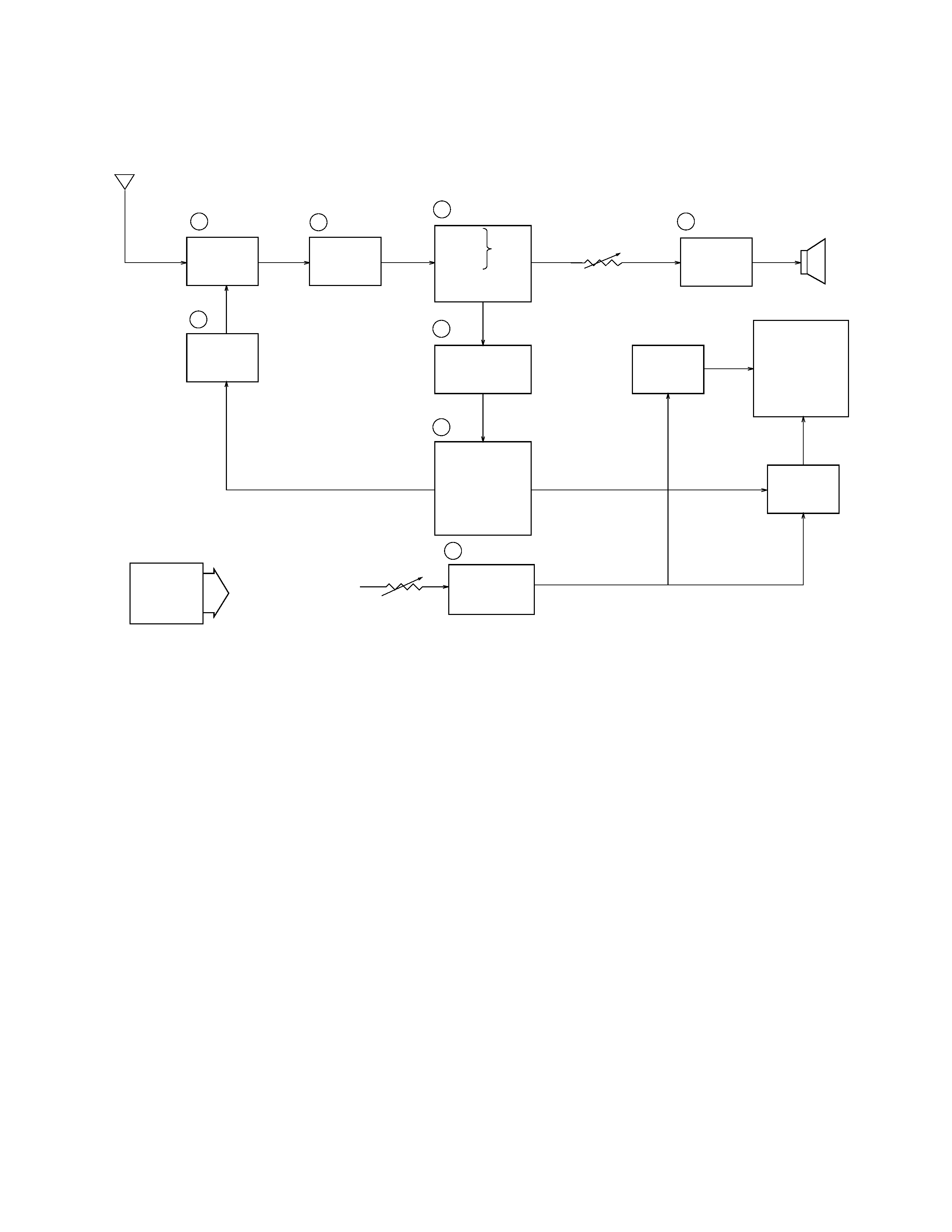
Antenna
1
TU200
2
Q200
3
IC200
7
Tuning
Voltage
Generator
VR600
Volume
Control
4
IC600
Speaker
IC300
IC700
Common
Driver
LCD
Segment
Driver
Chroma
Circuit
Osc.
Display
Control
A-D Converter
Auto-Tuning
Control
5
6
8
IC800, Q804~Q806, Q810, Q811
VR800
Display
Voltage
Generator
Brightness
Control
VCC2 (4.3±0.02V)
VCC7 (41.6~51.6V)
VEE1 (-6.5~-8.0V)
IC500
Power
Supply
Audio
Amp.
IF Amp.
Tuner
Video
Sound
Det.
FM
AFT Circuit
AGC Circuit
Det
1
-- Color Tuner: TU200 TEPU5-02
Selects a desired radio wave and changes it to the video IF signal.
2
-- Video IF Amp.: Q200 2SC4238
Amplifies the video IF signal output from the tuner TU by 10 times (20 dB).
3
-- Video Det./Sound Det./FM Det./AFT/AGC: IC200 M51348FP
Eliminates the carrier wave in the video IF signal, and picks up the video signal and the sound IF signal.
Also, the sound signal is picked up from the sound IF signal by FM detection.
4
-- Audio Amp.: IC600 NJM2070M
Sound amplification.
5
-- Chroma Circuit: IC300 M52042FP
Generates the tricolor (red, green, and blue) from the video signal.
6
-- Osc./A-D Converter/Display Control/ Auto-Tuning Control : IC700 MSM6625-01 GSK-640E
Converts the color signal into a digital signal.
Also, generates the clock pulse for the display and controls the display.
7
-- Tuning Voltage Generator: IC500 MSC1169MS-K
Generates the tuning voltage with the tuning pulse (TU) output from 6.
8
-- Display Voltage Generator: IC800 BA10358F, Q804 ~ Q806 Q810 Q811 2SD1149-S,
2SD601A-R
× 3, 2SB709A-R
Generates the display voltages V0 ~ V4 with VEE1 and VCC7 outputs from the power supply.
BLOCK DIAGRAM
Signal Name
Function
Signal Name
Function
D1 ~ D6
Display data output terminal
MTB
Mute control terminal
SNB
Data latch signal
TU
Tuning control pulse output terminal
CDB
Scanning start signal
VLB
VHF High/Low channel select signal
output terminal
CFB
Output voltage changeover signal
UHF
VHF/UHF select signal
CNB
Scanning signal shift lock signal
AVB
KCB
Key input terminal
KDB
SCB
Brightness modulation pulse control
AFT
AFT voltage input terminal
STB
Sampling start signal
M1 ~ M10
Mode select signal input terminal
ECB
Signal input terminal controlling the
TE1 ~ TE6
Test terminal
segment drive terminal to "H" during
no display
CK1, CK2
Clock pulse output terminal
R, G, B
Original color
OSC1
Oscillator freuency control terminal
RLL
"L" level voltage input terminal of
OSC2
video signal
PD
Clock pulse adjustment terminal
RHH
"H" level voltage input terminal of
video signal
C-S
Synchronizing pulse input terminal
PS1
Mode control signal
HDB
Horizontal synchronizing signal input
VSS1
Power supply voltage input terminal
terminal
VDD1
VDD voltage input terminal
-- 4 --
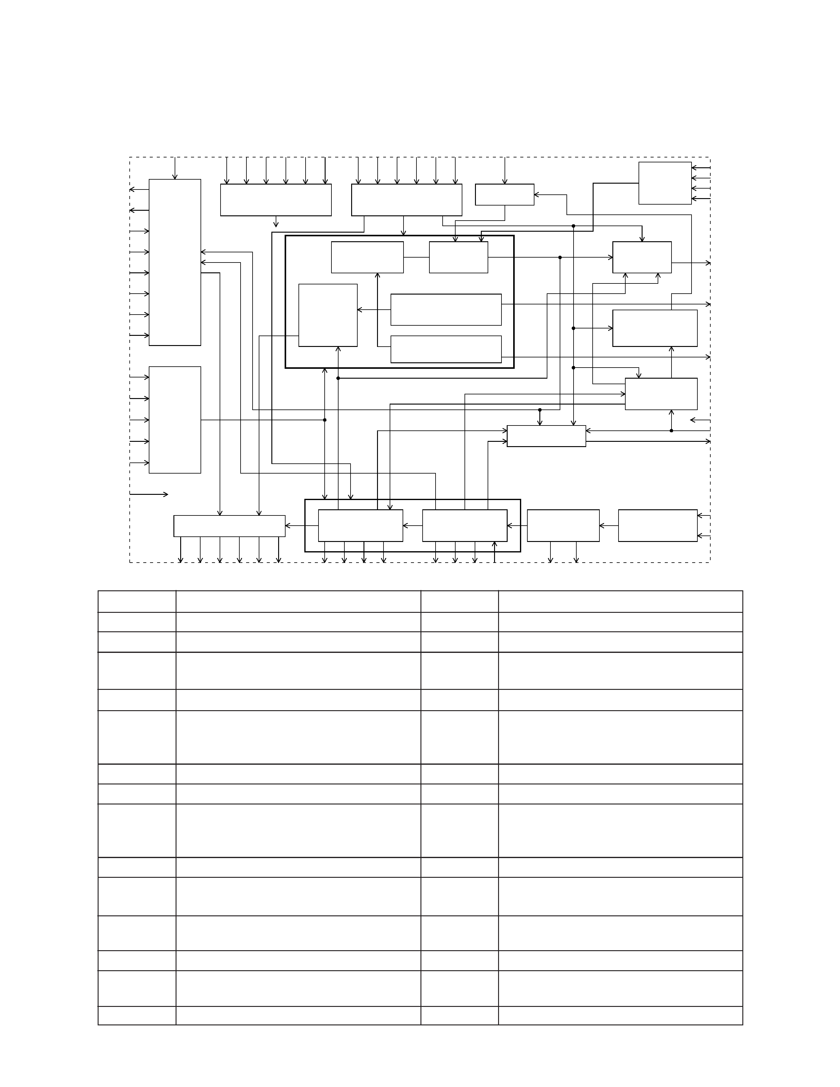
CIRCUIT OPERATION
IC700
AD2
AD1
R
G
B
RLL
VDD2
RHH
M7
M8
M9
M10
PSi
VSS1
A/D
Mode
Control
Test Control
Mode Control
AFT
Control
VSS2
TE1
TE2
TE3
TE4
TE5
TE6
M6 M5 M4 M3 M2 M1
AFT
KDB
KCB
UHF
AVB
MTB
VLB
TU
VDD1
C-S
PD
OSC1
OSC2
Key
Switch
Control
Mute
Control
Synchronism
Judgment
Frequency
Separator
Phase
Comparator
Oscillator
Frequency
Divider
Horizontal
positioning
Control
Vertical
positioning
Control
Data Output
Channel
bar
Control
Tuning Voltage
UP/DOWN Counter
Pulse Width
Modulation D/A
Sweep
Control
Frequency
Divider
Tuning Control
Test
Circuit
Display
Control
D1 D2 D3 D4 D5 D6
CDB CFB CNB ECB
SNB SCB STB HDB
CK1 CK2
-- 5 --
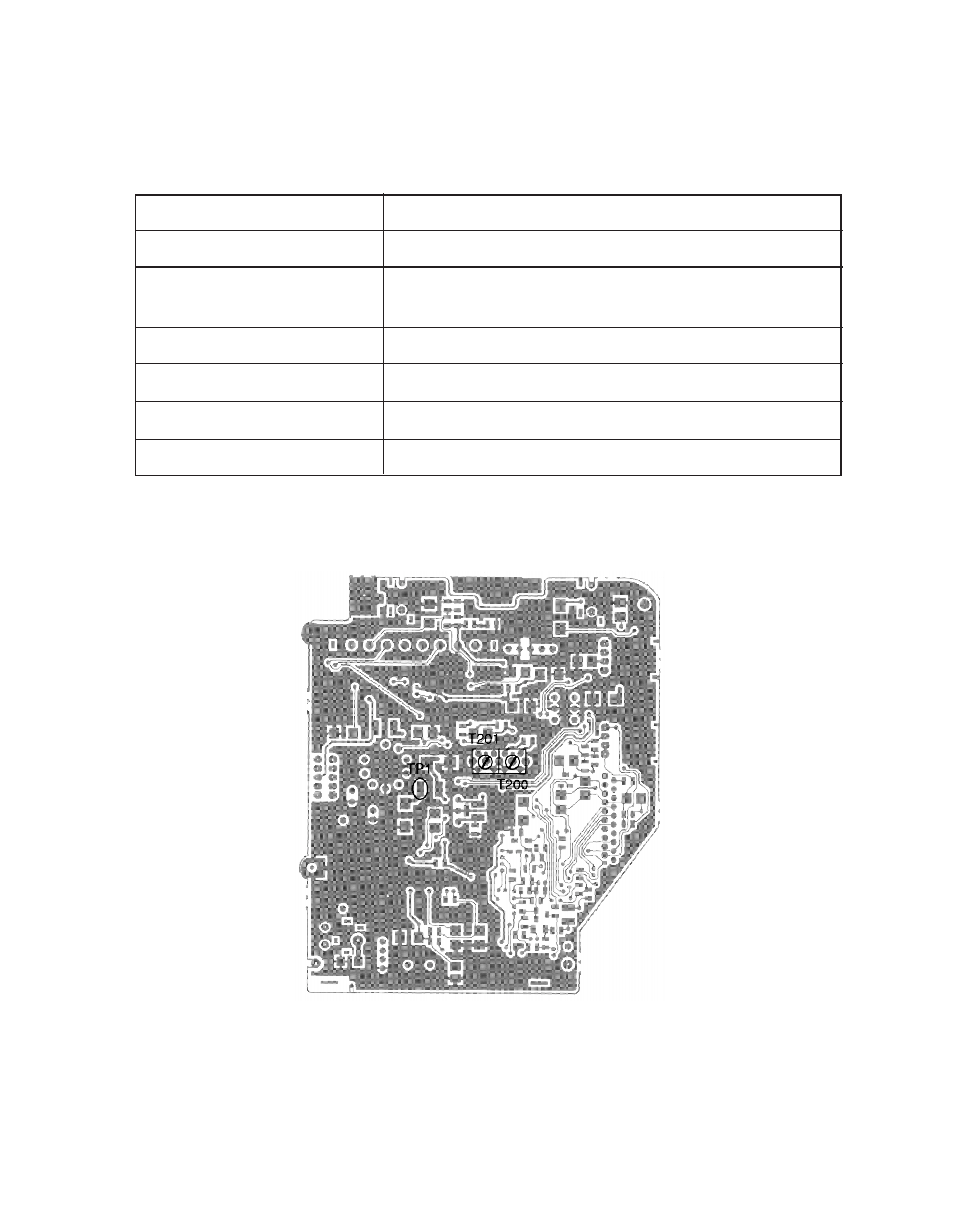
ADJUSTMENT
LINEAR PCB
1) Items To Be Adjusted
Item
Measuring Instrument
VCC2 voltage setting
Voltmeter
Video detection coil adjustment
TV signal generator, pattern generator, oscilloscope,
low-pass filter
AFT coil adjustment
Sweep generator, oscilloscope, voltmeter
Contrast adjustment
TV signal generator, pattern generator, oscilloscope
AGC adjustment
TV signal generator, pattern generator, IF levelmeter
Clock adjustment
Voltmeter
2) Adjustment And Test Point Locations
TOP VIEW