SF-8350R(LX-523)
JAN. 1994
R
(with price)
SF-8350R

CONTENTS
1.
SCHEMATIC DIAGRAM ................................................................................................ 1
2.
SPECIFICATIONS ......................................................................................................... 5
3.
TO REPLACE THE BATTERY ...................................................................................... 6
4.
ERROR MESSAGE ....................................................................................................... 7
5.
TO RESET THE DIGITAL DIARY ................................................................................. 7
6.
TO SAVE THE DATA TO OTHER MACHINE ............................................................... 8
7.
TO CHECK THE MEMORY CAPACITY ...................................................................... 11
8.
DISASSEMBLY ........................................................................................................... 12
9.
BLOCK DIAGRAM ...................................................................................................... 14
10.
CIRCUIT EXPLANATIONS
10-1.
System chart ................................................................................................. 15
10-2.
Power supply circuit .................................................................................... 16
10-3.
Battery voltage detection ............................................................................ 19
10-4.
CPU pin description (
µPD3055GF002-2BA) ............................................... 21
10-5.
Gate array pin descriptions (
µPD65005G-452-22) ..................................... 21
10-6.
Power supply chip IC pin descriptions (SC371015FU) ............................. 21
10-7.
Character generator ROM pin descriptions (HD62063B01) ..................... 22
10-8.
Operation program ROM pin descriptions (
µPD23C2001EGW342) ......... 23
10-9.
RAM pin descriptions (
µPD43256AGU-10/12/15LL) .................................. 23
11.
DIAGNOSTIC OPERATION ........................................................................................ 24
12.
TROUBLE SHOOTING ................................................................................................ 29
13.
PARTS LIST ................................................................................................................ 32
14.
PCB VIEW ................................................................................................................... 34
15.
ASSEMBLY VIEW ....................................................................................................... 35
-- 1 --
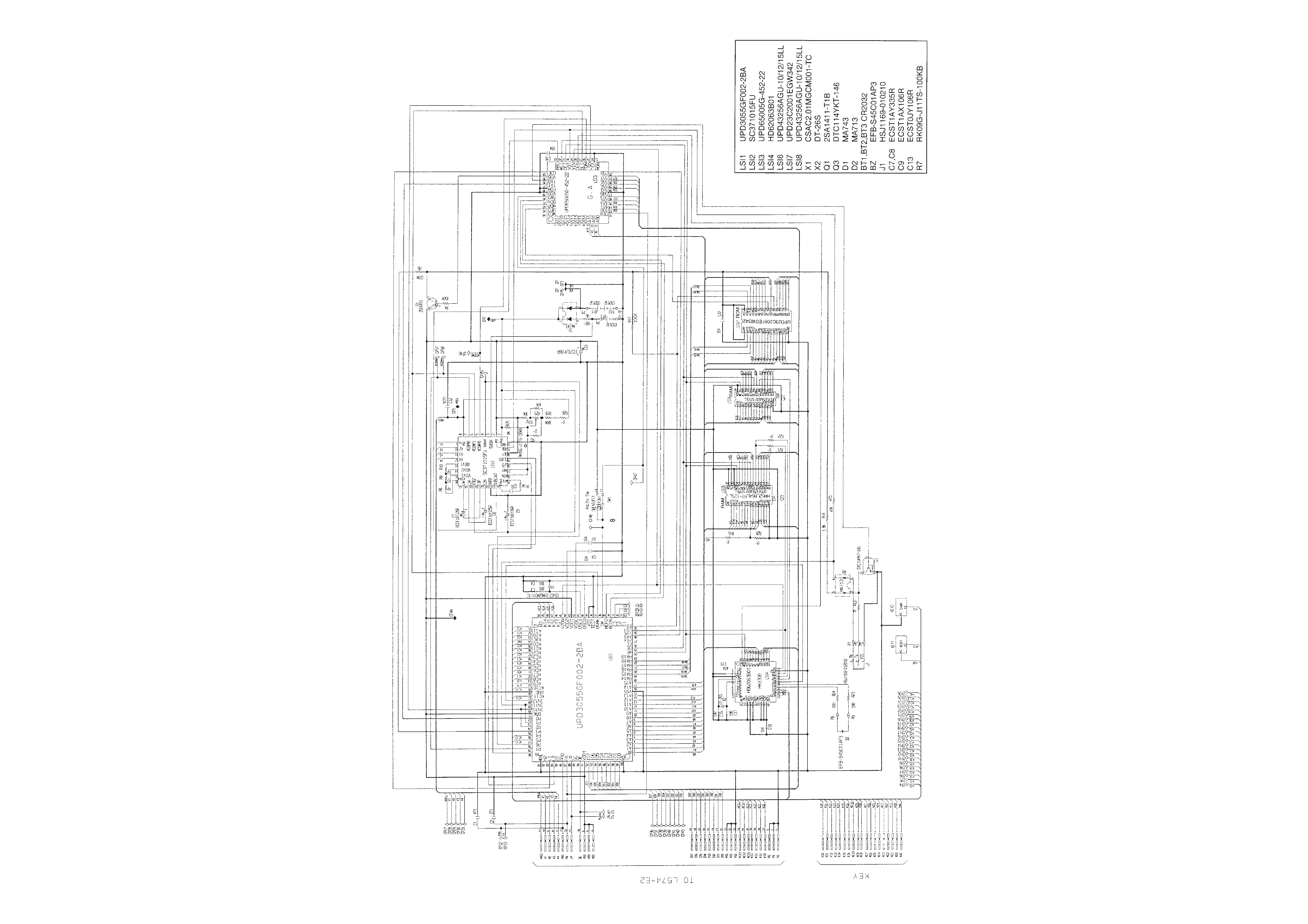
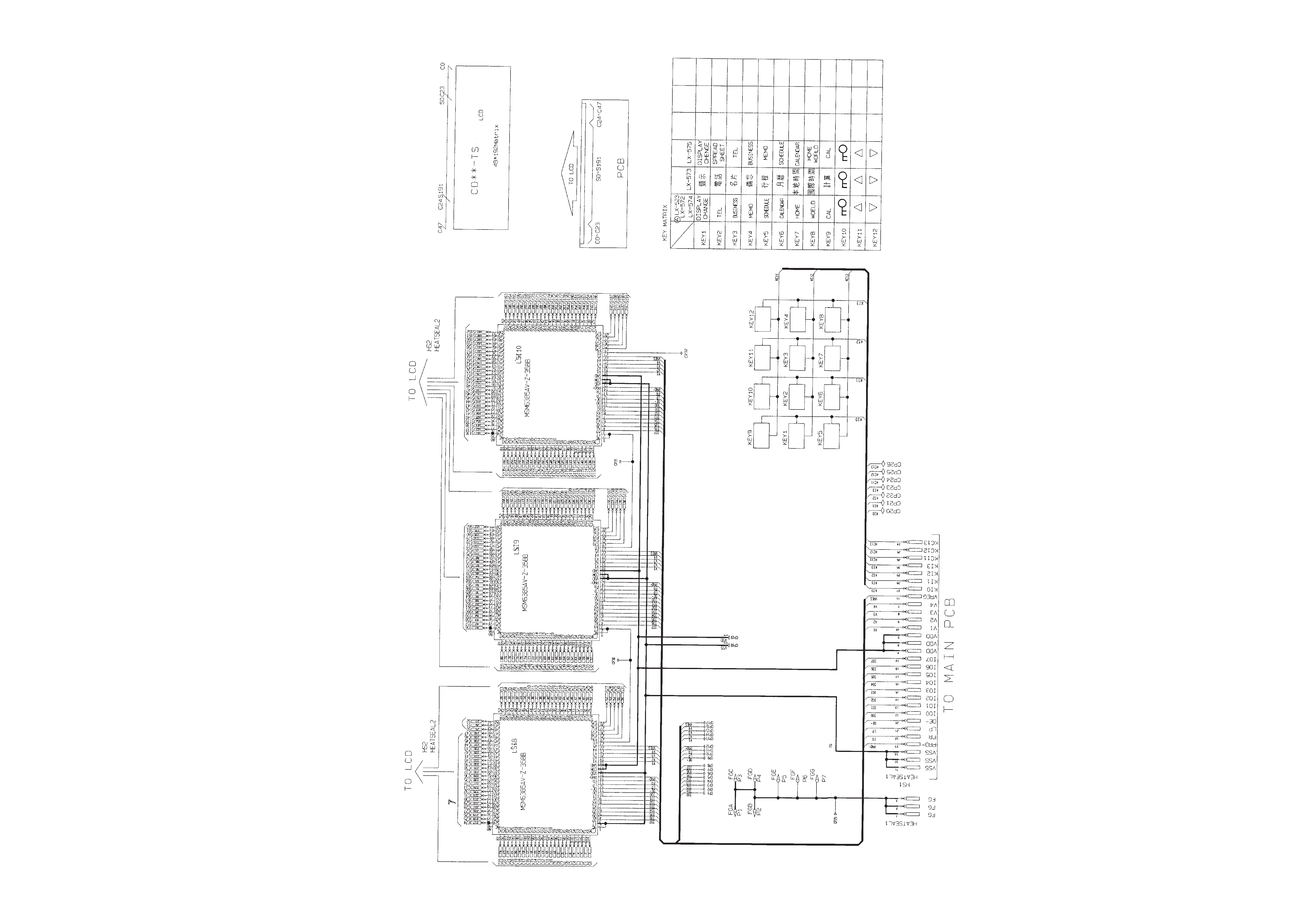
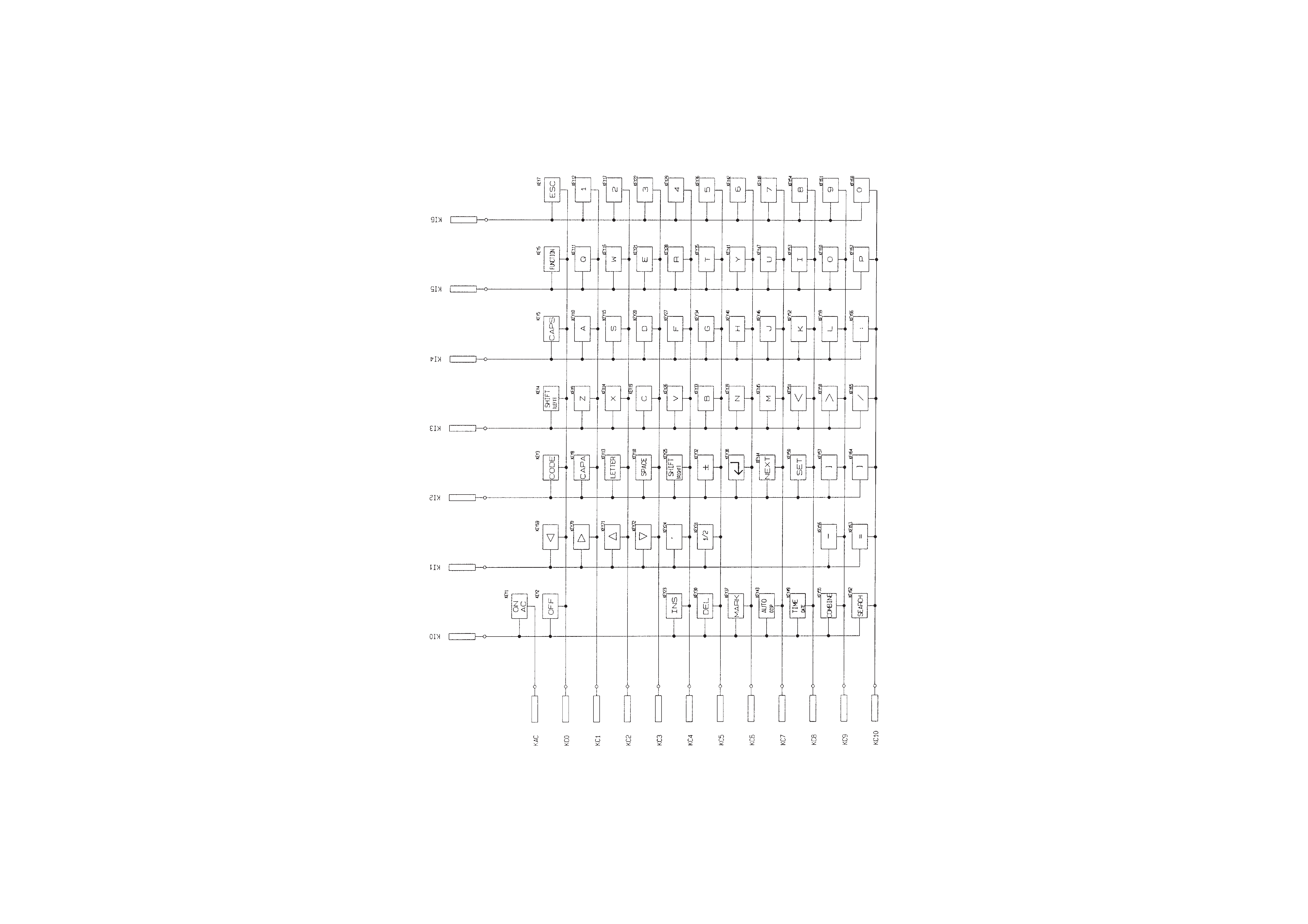
1.
SCHEMATIC DIAGRAM
1-1. Main PCB
-- 2 --
1-2. Display PCB
-- 3 --
1-3. Key Matrix