R
QV-700
JAN. 1998
(without price)
(KX-772)

CONTENTS
SPECIFICATIONS ...................................................................................................................................... 1
WIRING AND BLOCK DIAGRAM ..............................................................................................................2
POWER SUPPLY CIRCUIT OPERATION ..................................................................................................3
ADJUSTMENT ........................................................................................................................................... 4
1. Unit Adjustment .................................................................................................................................... 4
1-1. Color parameters loading ............................................................................................................4
1-2. Scratch compensation .................................................................................................................5
1-3. Flash adjustment ..........................................................................................................................5
1-4. Flash check ...................................................................................................................................6
1-5. Current consumption ...................................................................................................................7
1-6. Clock reset .................................................................................................................................... 7
1-7. Other test modes ..........................................................................................................................8
2. PCB K772-DA Adjustment .................................................................................................................... 8
2-1. VCC1, VCC3 voltage check ..........................................................................................................9
2-2. VCC7, VEE3 adjustment ............................................................................................................... 9
2-3. Clock oscillation check ................................................................................................................ 9
3. PCB K77-L Adjustment ....................................................................................................................... 10
3-1. VCC1 adjustment and VCC2, VCC6, VEE2, VCC0 voltage check ........................................... 11
3-2. VCO free run frequency adjustment ......................................................................................... 11
3-3. Backlight drive voltage adjustment ..........................................................................................12
3-4. VCOM AC adjustment and VCOM DC coarse adjustment ......................................................12
3-5. Brightness voltage setting and contrast adjustment .............................................................. 13
3-6. Color adjustment ........................................................................................................................14
3-7. TINT adjustment ..........................................................................................................................15
3-8. VCOM DC adjustment .................................................................................................................15
DISASSEMBLY ........................................................................................................................................ 16
PRINTED CIRCUIT BOARDS .................................................................................................................. 22
EXPLODED VIEW .................................................................................................................................... 26
PARTS LIST ............................................................................................................................................. 28
SCHEMETIC DIAGRAMS ........................................................................................................................34
-- 1 --
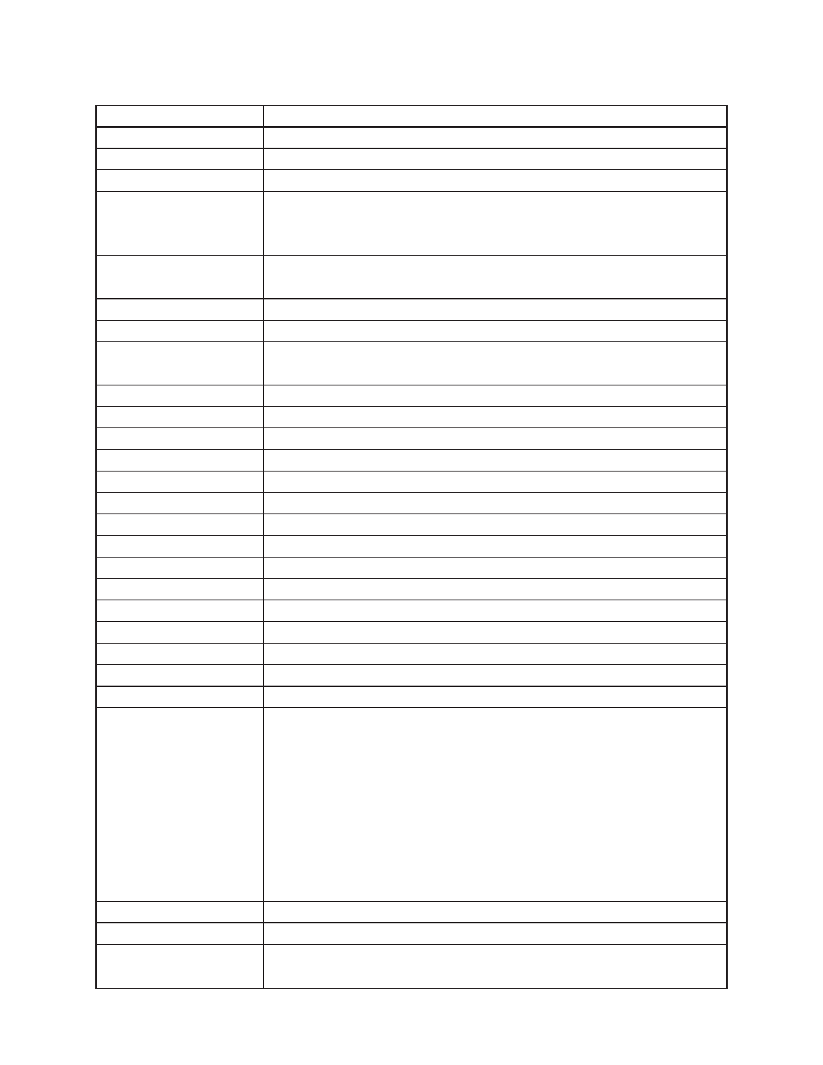
Item
Specification
Recording System
Digital (JPEG base)
Signal System
NTSC
Recording Medium
Memory card (2 MB card included)
Memory Capacity
FINE; 14 images (Approx. 133 KB compressed)
(2MB card)
NORMAL; 26 images (Approx. 70 KB compressed)
ECONOMY; 47 images (Approx. 38 KB compressed)
Image Deletion
Single image; all images in a folder, all images in memory (with image pro-
tection)
Imaging Element
1/4-inch CCD (350,000 pixels)
Lens
Fixed focal point with macro position; F2, f = 3.94 mm
Focus Range
NORMAL: 70 cm to
MACRO: 14 cm to 16 cm (from surface of protective lens)
Light Metering
TTL center priority by CCD
Exposure Metering
Program AE
Exposure Range
EV +5 to 18
Exposure Correction
2 EV to +2 EV
Shutter
CCD shutter
Shutter Speed
1/8 to 1/4000 second
White Balance
Automatic
Self-timer
10 seconds, 2 seconds
Flash Modes
Auto Flash, Flash On, Flash Off
Resolution Modes
FINE, NORMAL, ECONOMY
Monitor
2.5" TFT, low-glare color LCD (84,480 pixels)
Computer output image
480 x 640 pixels
Input/Output Terminals
DIGITAL IN/OUT, VIDEO OUT, AC adaptor connector, memory card connector
Clock
January 1, 1997 00:00:00 to December 31, 2049 11:59:59 (Auto calendar)
Power Supply
Four batteries (AA-size alkaline or lithium batteries) AC adaptor (AD-C620)
Battery Life
Continuous Playback:
Alkaline Batteries (LR6); Approx. 160 minutes
Lithium Batteries (FR6); Approx. 270 minutes
Continuous Recording:
Alkaline Batteries (LR6); Approx. 600 shots
Lithium Batteries (FR6); Approx. 1,200 shots
Note: The above values are obtained based on Panasonic's alkaline batter-
ies and Fujifilm's lithium batteries. For your reference, the values when the
camera is operated with Duracell's alkaline batteries are shown below.
Auto Play: Approximately 80 minutes
Continuous Recording: Approximately 170 images
Dimensions
147(W)
× 69(H) × 50(D) mm/5.8"(W) × 2.7"(H) × 2.0"(D)
Weight
Approximately 290 g/10.2 oz (excluding batteries)
Accessories
Memory card, wrist strap, soft case, special video cable, Alkaline batteries
(AA-size
× 4)
SPECIFICATIONS
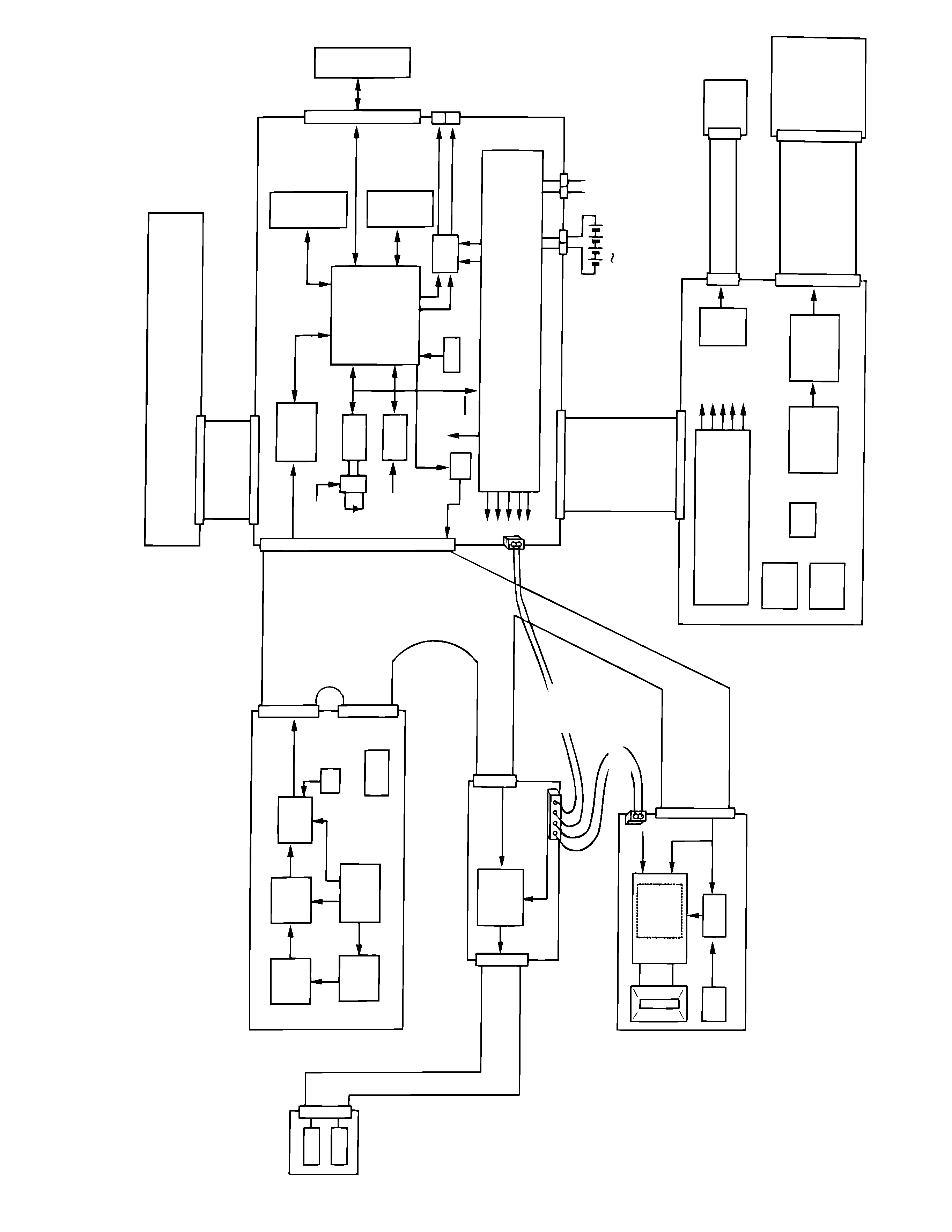
-- 2 --
WIRING
AND
BLOCK
DIAGRAM
Photo
INT
Auto
Iris
Lens
Solenoid
CB-PCB
ICX098AK
15V
CCD
15V
-5.5V
Vdrv
CXD1267AN
3.5V
CXA2056Q
CDS+AGC
CXD2310R
ADC
3.5V
BR9040F
EEROM
T.G
3.3V
CXD2452R
20-pin
23-pin
8-pin
KEY-PCB
DA-PCB
60-pin
3.3V
YUV
Processor
CXD3120R
3.3V
3.0V
Switching
RS5C316A
RTC
UPD6466
OSD
MB91181
Detection
Switch
3.3V
MACO
3.2V
INTR
CFDET
Signal
Generator
Video
RS232C
EDO_
DRAM
Flash
Memory
3.3V
3.3V
3.3V
15.0V
-5.5V
5.0V
Battery
Voltage
Voltage
Controller
5V
VIDEO
RS232C
3.3V
CF
AC
Adaptor
6.0V
10-pin
3.0V
4.5V
18.0V
12.0V
-10.5V
Trans-
former
5-pin
Battery
voltage
GND
Battery
voltage
GND
7-pin
Strobe
Ass'y
Comparator
Photo
Sensor
Xenon
Lamp
Battery
Voltage
Voltage
Controller
Detection
Sw.
(RSTW)
FUNC
button
LED
Chroma
IR3Y18A
Display
Controller
CM7013L2
4.5V
3V
26-pin
BL
LCD
module
High
Voltage
Generator
5-pin
CA-PCB
Motor
Driver
IRISA/IRISB
Battery
Voltage
L-PCB
3.3V
7-pin
3.3V
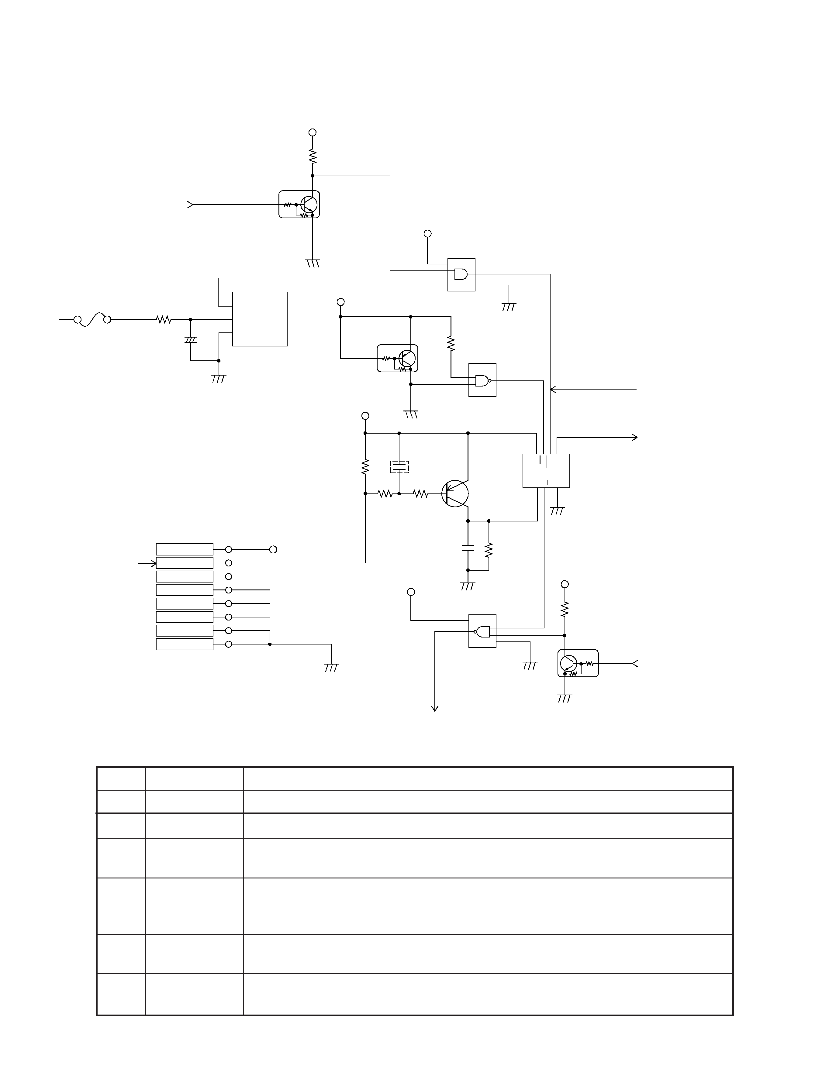
-- 3 --
1
2
3
4
5
6
7
8
VCC1-1
IC582
IC582
VCC1-1
VCC3-1
VCC3-1
PON
KEY0
KEY1
KEY2
SHTTER
GND
GND
CN504
R593
C592
R592
1
2
3
4
8
7
6
5
R594
R585
Q588
R595
R579
Q583
2
2
3
1
3
1
C590
VCC1-1
Q582
1
3
2
5
4
IC584
IC586
1
2
3
FU152
R590
C525
+
OUT
VDD
GND
NC
NC
CK
D
Q
GND
VCC
PR
CLR
Q
1 PON from
Key PCB
VCC1-1
Q580
1
2
3
2 APO from Pin 202
of IC500
6 Voltage detection signal
3 POB to Pin193
of IC500
4 FACT from
Pin 195 of IC500
IC588
VCC1-1
VCC1-1
VCC
GND
VCC
GND
5
1
2
3
4
6
5
4
3
8
5 Power ON to Pin 1 of Q155
1
2
7
POWER SUPPLY CIRCUIT OPERATION
1
2
3
4
5
6
Signal
PON
APO
POB
FACT
Power On
Voltage
detection
Operation
Power on/off signal (pulse) from Key PCB
Auto power off signal (pulse) from pin 202 of IC500
Power on/off recognition signal to pin 193 of IC500
ON: H (VCC3)
OFF: L (GND)
Forced power on signal from pin 195 of IC500
Forced ON: H (VCC3)
OFF: L (GND)
ex. While writing to flash memory
Power on/off signal to pin 1 of Q155
ON: H (VCC1)
OFF: L (GND)
Normal: H
Low voltage: L