TDE1707
INTELLIGENT POWER SWITCH
ADVANCE DATA
0.5A OUTPUT CURRENT
LOW SIDE OR HIGH SIDE SWITCH CON-
FIGURATION
6V TO 48V SUPPLY VOLTAGE RANGE
OVERLOAD AND SHORT CIRCUIT PROTEC-
TIONS
INTERNAL VOLTAGE CLAMPING
SUPPLY AND OUTPUT REVERSAL PRO-
TECTION
THERMAL SHUTDOWN
GND AND VS OPEN WIRE PROTECTION
ADJUSTABLE DELAY AT SWITCH ON
INDICATOR STATUS LED DRIVER
+5V REGULATED AUX. VOLTAGE
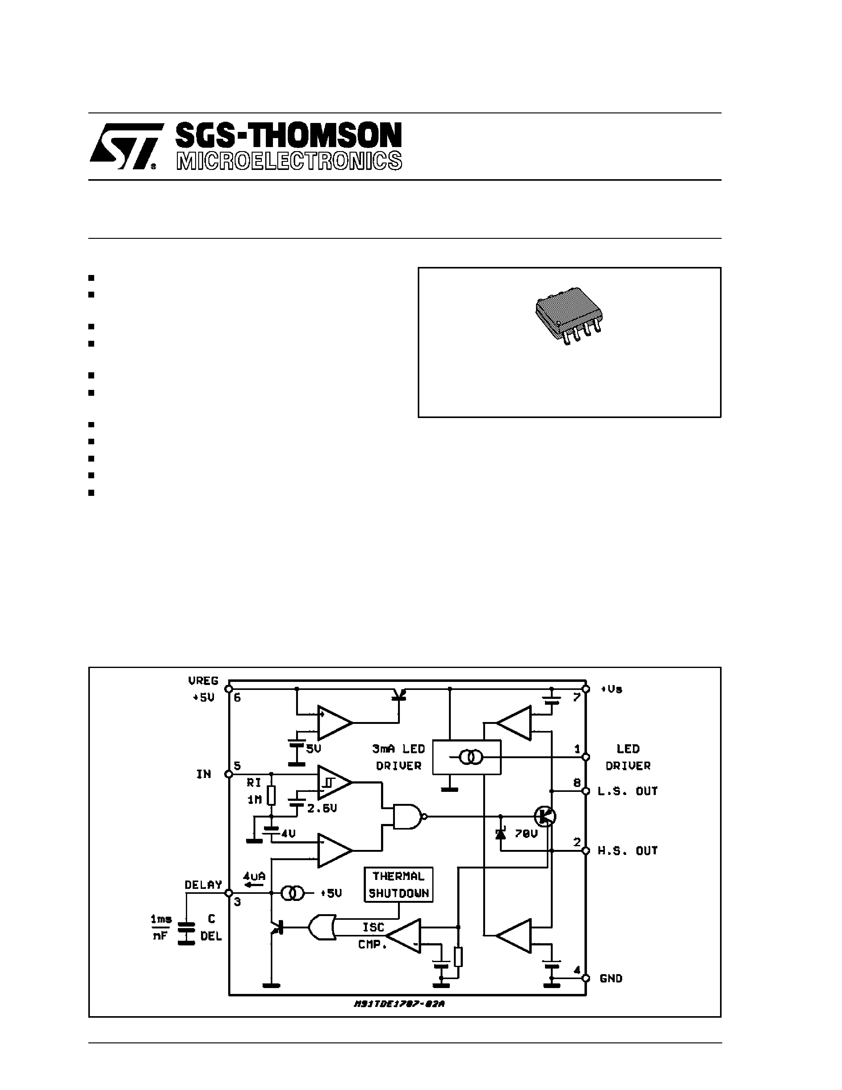
DESCRIPTION
The TDE1707 is a 0.5A Integrated Power Switch
with up to 48V Power supply capability.
Two output configurations are possible:
- Load to Gnd. (High Side Mode)
- Load to VS (Low side Mode)
Especially dedicated to proximity detectors, its in-
ternal +5V supply can be used to supply external
circuits (See also AN495/0692). A signal is inter-
nally generated to block the In signal, and prevent
activation of the output switch, as long as an ab-
normal condition is detected. The power-on tran-
sition, as well as the chip overtemperature and
the output overcurrent, concurr to the generation
of such signal. A minimum delay of 25
µs (Typ.
value) is added to the trailing edge of such signal
to ensure that a stable normal situation is present
when the signal disappears. The delay (of the dis-
apperance of the block signal; no delay at its on
set) can be further increased connecting a ca-
pacitor between pin3 and ground. It can drive re-
sistive or inductive loads.
This is advanced information on a new product now in development or undergoing evaluation. Details are subject to change without notice.
July 1992
SO8
ORDERING NUMBER: TDE1707FP
BLOCK DIAGRAM
1/6
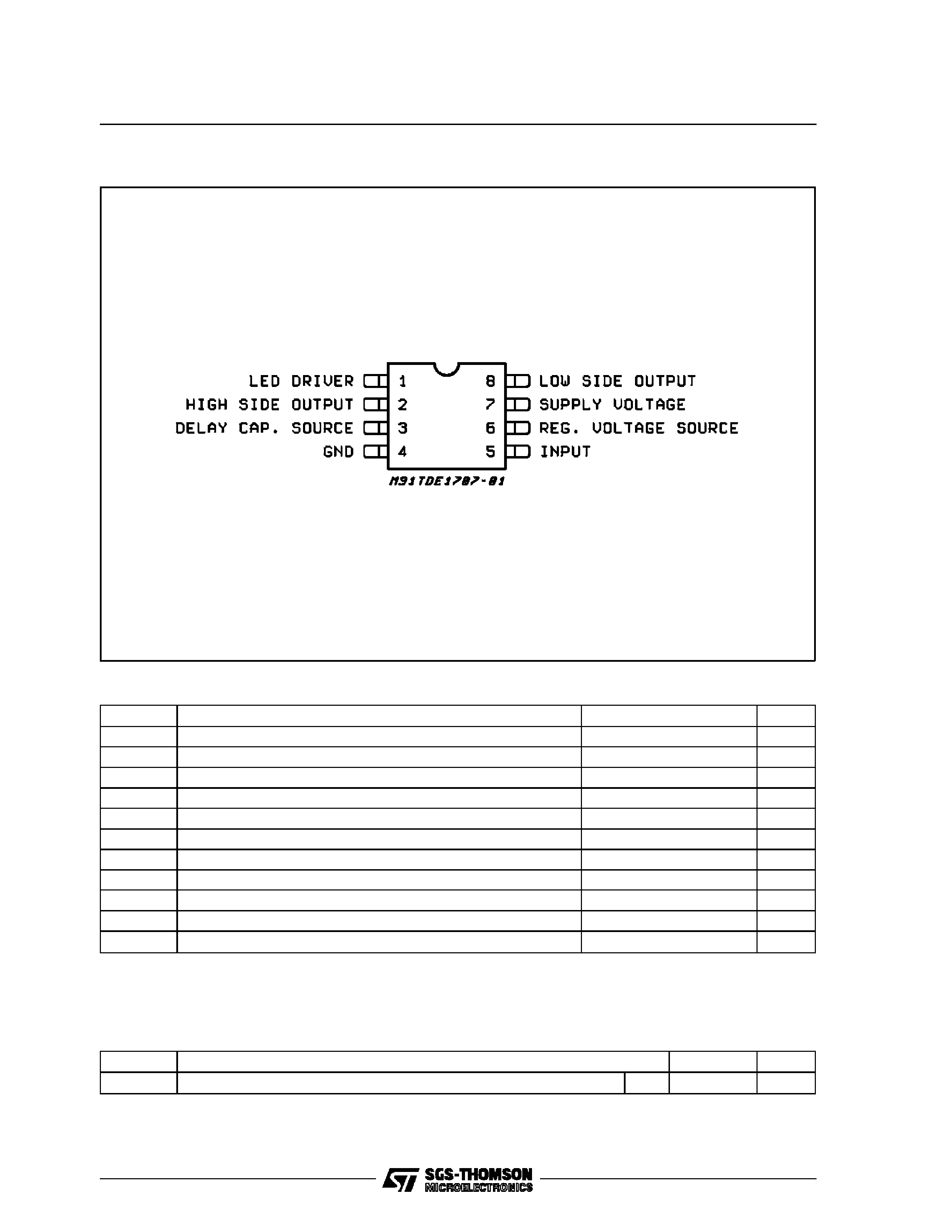
PIN CONNECTION (Top view)
ABSOLUTE MAXIMUM RATINGS
Symbol
Parameter
Value
Unit
VS
Supply Voltage
50
V
VSr
Supply Reverse Voltage
50
V
IO
Output Current
internally limited
A
Vreg
Regulated Voltage Pin
0 to 7
V
Vdelay
Delay Cap. Surce Pin
0 to 5
V
VO
Output Diff. Voltage
55
V
Vi
Input Voltage
-10 to 50
V
Top
Operating Temperature Range
-25 to +85
°C
Tstg
Storage Temperature
-55 to 150
°C
Ptot
Power Dissipation
internally limited
W
El
Energy Induct. Load
150
mJ
THERMAL DATA
Symbol
Description
Value
Unit
Rth j-amb
Thermal Resistance Junction-ambient
Max.
150
°C/W
TDE1707
2/6
ELECTRICAL CHARACTERISTICS (VS = 24V; Tj = 25 to +85
°C, unless otherwise specified)
Symbol
Parameter
Test Condition
Min.
Typ.
Max.
Unit
Vs 7
Supply Voltage
6
48
V
Isr 7
Supply Reverse Current
VSR = 48V
1.5
mA
Iq 7
Quiescent Current
Ireg =Iled =0; Vi < 2V;
VS = 6 to 48V
1.5
mA
Io 8/2
Output Current
Vs = 6V to 32V
500
mA
Io 8/2
Output Current
Vs = 32V to 48V
300
mA
Vsat 8/2
Output Voltage Drop V8-2
Io = 500mA
1.1
1.6
V
Vsat 8/2
Output Voltage Drop V8-2
Io = 300mA
1.5
V
Isc 8/2
Short Circuit Current
0.5
0.8
2
A
Vcl 8/2
Internal Voltage Clamp
ICL = 10mA
55
65
V
Iolk 8/2
Output Leakage
0
(Pin 2)
Vi < 2V; Vo = 0 to Vs (Pin 8)
100
300
100
µA
µA
Vith 5
Input Voltage Threshold
2
3
V
Vihis 5
Input Threshold Hysteresis
300
mV
Ilk 5
Input Current
Vi =5V
2
5
µA
Vreg 6
Regulated Output Voltage
Ireg < 5mA
4.5
5
5.5
V
Iscr 6
Short Circuit Regulated
6
30
50
mA
Ireg 6
Ouput Regulator Current
Vs = 35V
Vs = 48V
6
4
mA
mA
Iold 1
Current Surce Sink Led Driver
Output ON (
±)2
3
4
mA
Vold 1
Voltage Drop Led Driver
Ios = 2mA (
±)
1.2
1.6
V
Oldlk 1
Lead Driver (off) Leak.
Vi < 2V; RL <1K
10
µA
Idch 3
Del. Cap. Charge Current
TJ =25
°C2
4
6
µA
Vdth 3
Delay Voltage Trigger
TJ =25
°C4
V
DYNAMIC CHARACTERISTICS (VS = 24V; RL =48
;TJ =25°C)
ton
Propagation Turn on Time
Vi = 0 to 5V
15
µs
toff
Propagation Turn off Time
Vi = 5 to 0V
15
µs
tdon
Delayed Turn on Time / nF
Delay Capacitor
0.65
1
2
ms
td min
Minimum Delayed ton
Delay Capacitor = 0
25
µs
APPLICATION INFORMATION (See Application
Circuit)
The LED driver tells the output status.
It can source or sink current (Iold typ = 3mA), ac-
cording to the output configuration chosen.
The thresholds, represented by the output com-
parator in the Block Diagram, are set at about
1.5V - 2V.
For instance, in the High Side Load case of the
Application Circuit, when the voltage on pin 8 (the
output) differs from VCC less than 1.5V, the output
is sensed in "OFF" state and the LED driver is
disabled.
If instead pin 8 differs from VCC more than 3V (the
output comparator threshold value plus the drop
voltage on the LED), then the output is sensed
"ON" and the driver will force the current on the
LED.
TDE1707
3/6
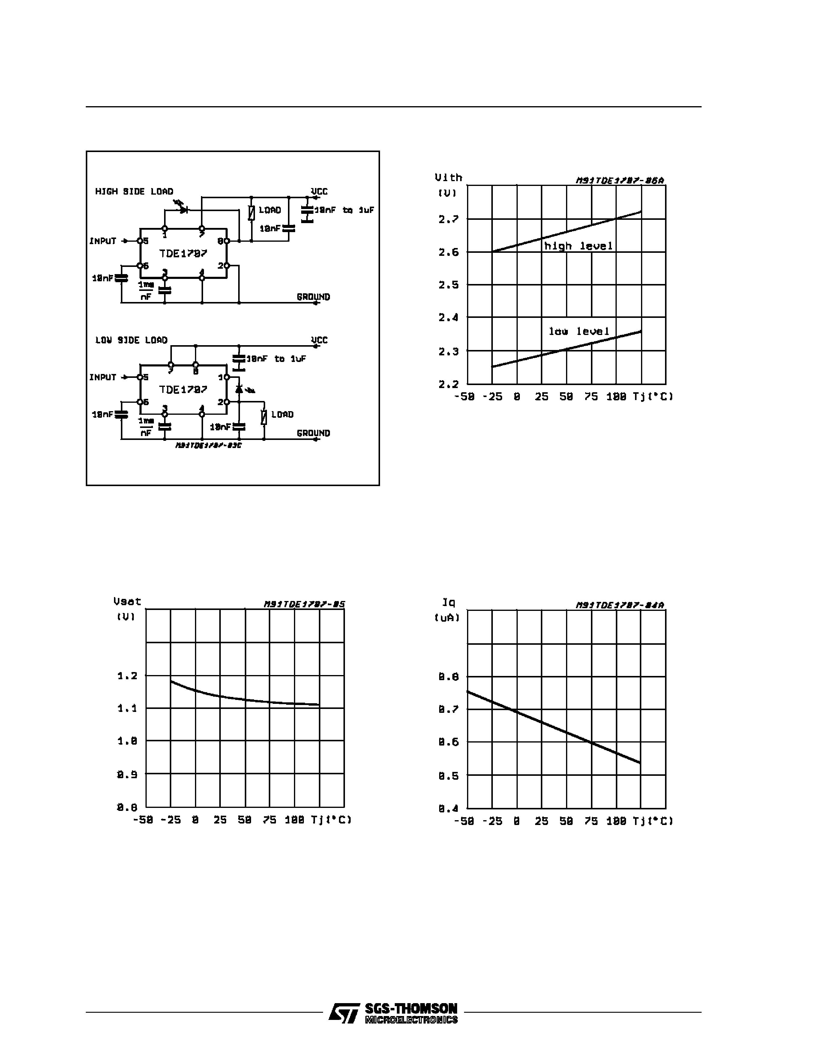
APPLICATION CIRCUIT
Figure 1: Input Thresholds Voltage vs.
Temperature (VS = 24V)
Figure 2: Saturation Voltage vs. Temperature
(VS = 24V; IO = 500mA)
Figure 3: Quiescent Current) vs.Temperature
(VS = 24V)
TDE1707
4/6
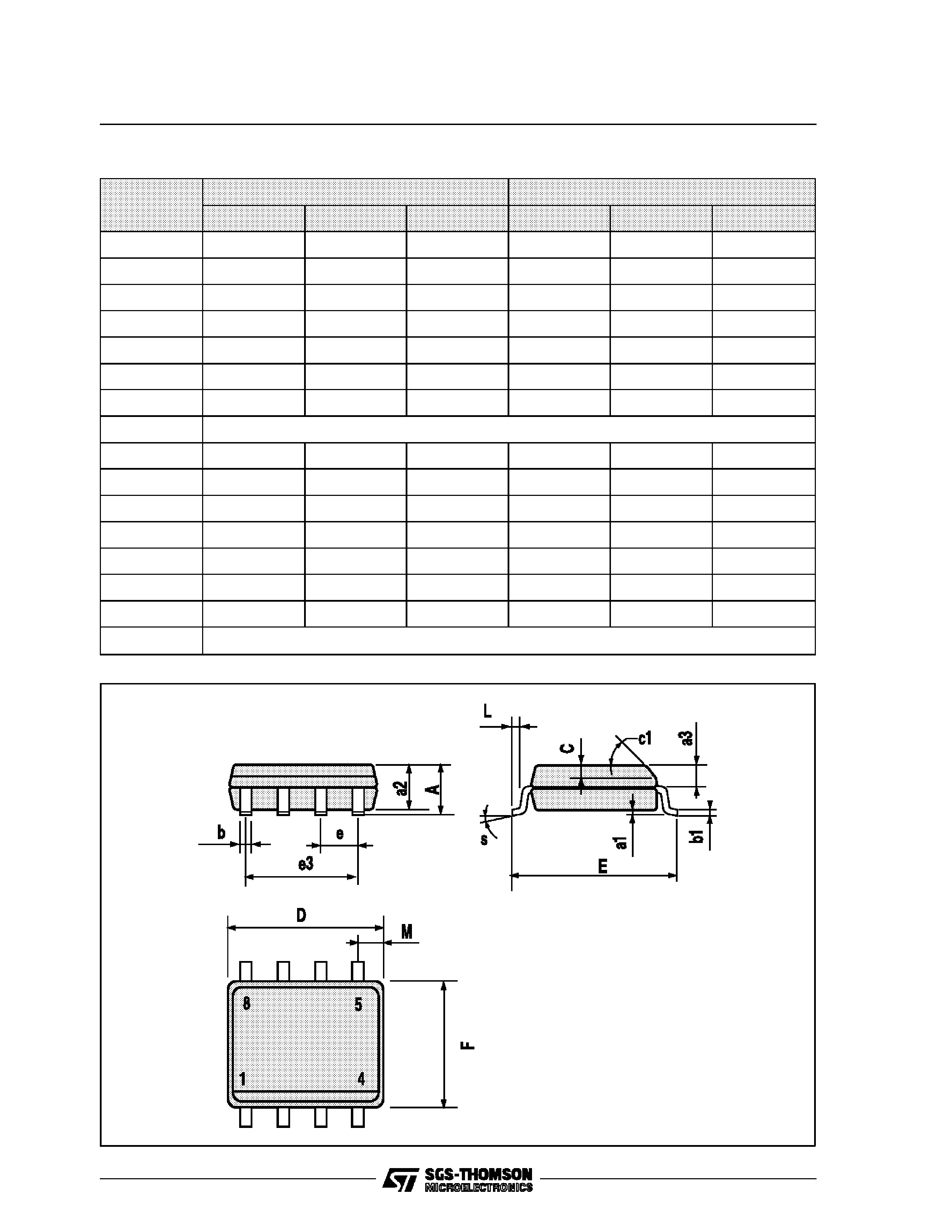
SO8 PACKAGE MECHANICAL DATA
DIM.
mm
inch
MIN.
TYP.
MAX.
MIN.
TYP.
MAX.
A
1.75
0.069
a1
0.1
0.25
0.004
0.010
a2
1.65
0.065
a3
0.65
0.85
0.026
0.033
b
0.35
0.48
0.014
0.019
b1
0.19
0.25
0.007
0.010
C
0.25
0.5
0.010
0.020
c1
45
° (typ.)
D
4.8
5.0
0.189
0.197
E
5.8
6.2
0.228
0.244
e
1.27
0.050
e3
3.81
0.150
F
3.8
4.0
0.15
0.157
L
0.4
1.27
0.016
0.050
M
0.6
0.024
S8
° (max.)
TDE1707
5/6