L7800AB/AC
SERIES
January 1993
PRECISION 1A REGULATORS
.
OUTPUT CURRENT IN EXCESS OF 1A
.
OUTPUT VOLTAGES OF 5; 6; 8; 9; 12; 15; 18;
24V
.
THERMAL OVERLOAD PROTECTION
.
SHORT CIRCUIT PROTECTION
.
OUTPUT TRANSISTOR SOA PROTECTION
.
2% OUTPUT VOLTAGE TOLERANCE
.
GUARANTEED IN EXTENDED TEMPERA-
TURE RANGES
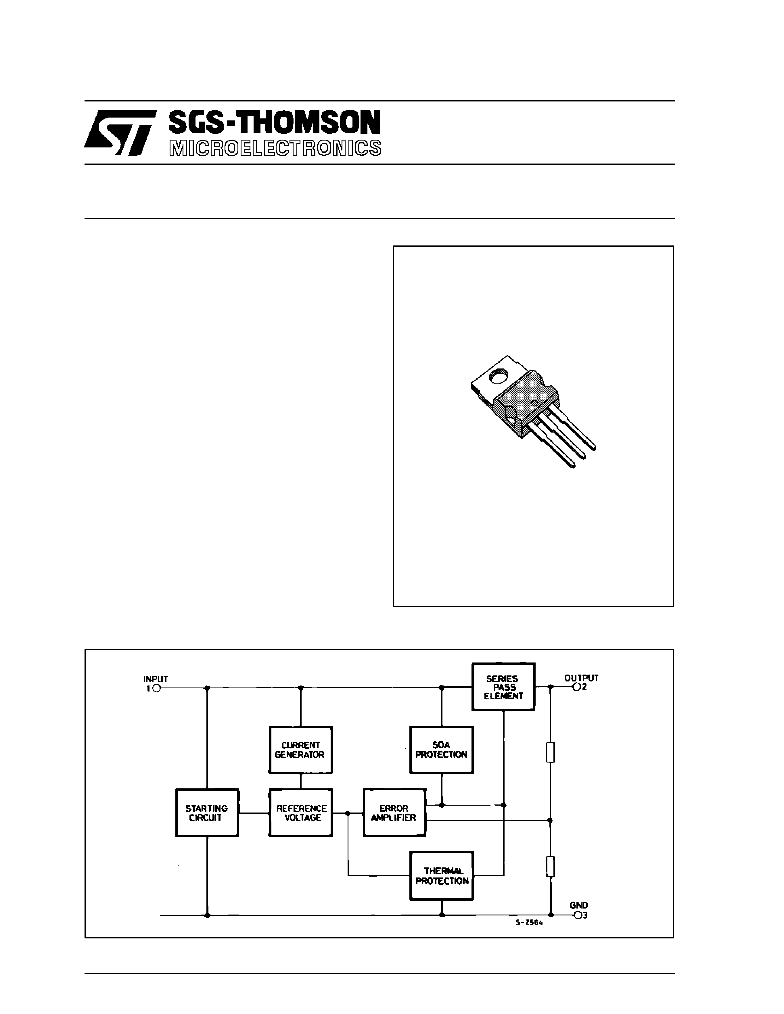
DESCRIPTION
The L7800A series of three-terminal positive regu-
lators is available in TO-220 and TO-3 packages
and with several fixed output voltages, making it
useful in a wide range of applications. These regu-
lators can provide local on-card regulation, eliminat-
ing the distribution problems associated with single
point regulation. Each type employs internal current
limiting, thermal shut-down and safe area protec-
tion, making it essentially indestructible. If adequate
heat sinking is provided, they can deliver over 1A
output current. Although designed primarily as fixed
voltage regulators, these devices can be used with
external components to obtain adjustable voltages
and currents.
TO-220
BLOCK DIAGRAM
1/14
ABSOLUTE MAXIMUM RATINGS
Symbol
Parameter
Val ue
Unit
Vi
DC Input Voltage (for Vo = 5 to 18V)
(for Vo =24V)
35
40
V
V
I o
Output Current
Internally limited
Ptot
Power Dissipation
Internally limited
T j
Operating Junction Temperature for L7800AC
for L7800AB
0to 125
40 to 125
°C
°C
T stg
Storage Temperature
65 to + 150
°C
THERMAL DATA
Symbol
Parameter
Value
Unit
Rthj-case
Rthj-amb
Thermal Resistance Junction-case
Max
Thermal Resistance Junction-ambient
Max
3
50
oC/W
oC/W
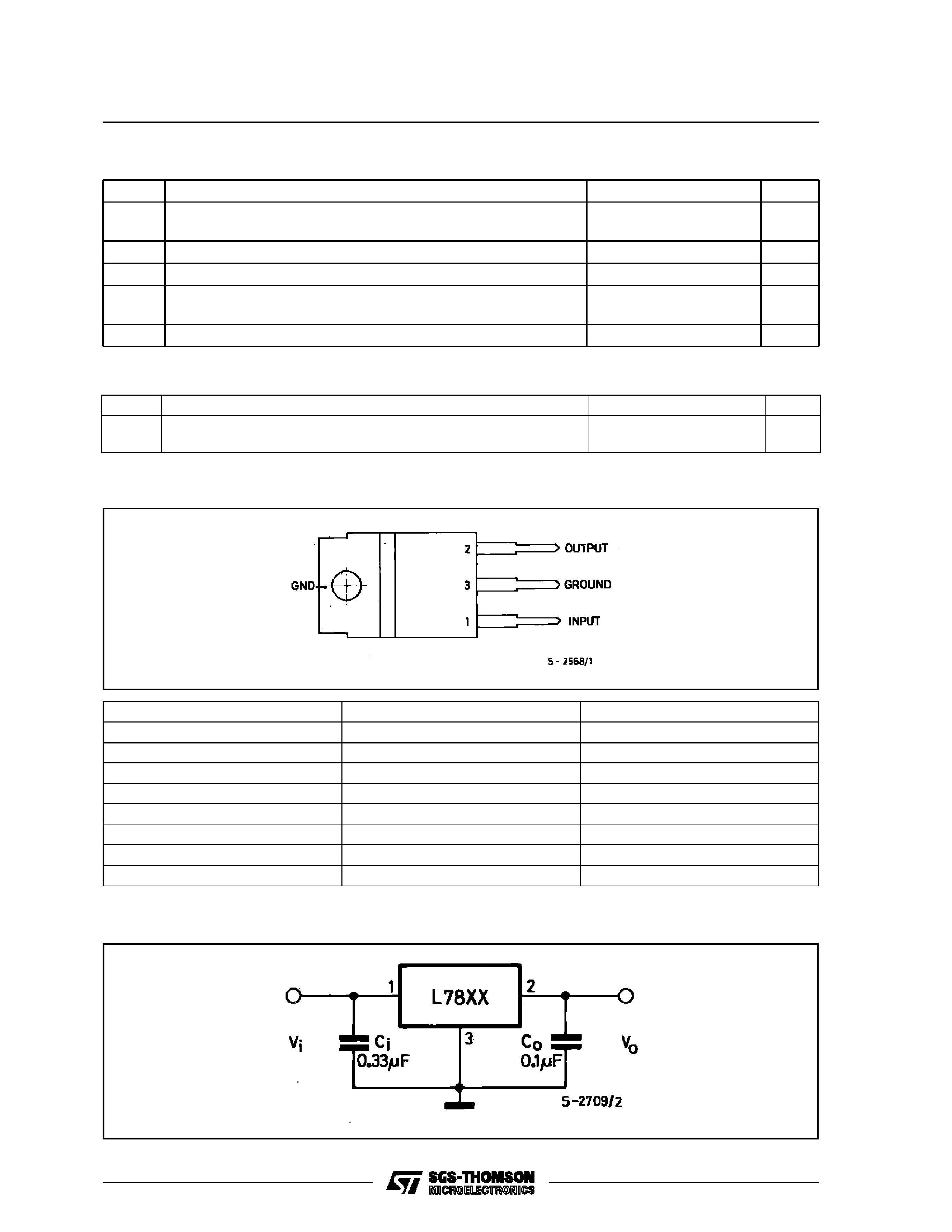
CONNECTION DIAGRAM AND ORDERING NUMBERS (top view)
TO-220 (Tj = -40 to 125
oC)
TO-220 (Tj = 0 to 125
oC)
Output Voltage
L7805ABV
L7805ACV
5V
L7806ABV
L7806ACV
6V
L7808ABV
L7808ACV
8V
L7809ABV
L7809ACV
9V
L7812ABV
L7812ACV
12V
L7815ABV
L7815ACV
15V
L7818ABV
L7818ACV
18V
L7824ABV
L7824ACV
24V
TYPICAL APPLICATION
L7800AB/AC SERIES
2/14
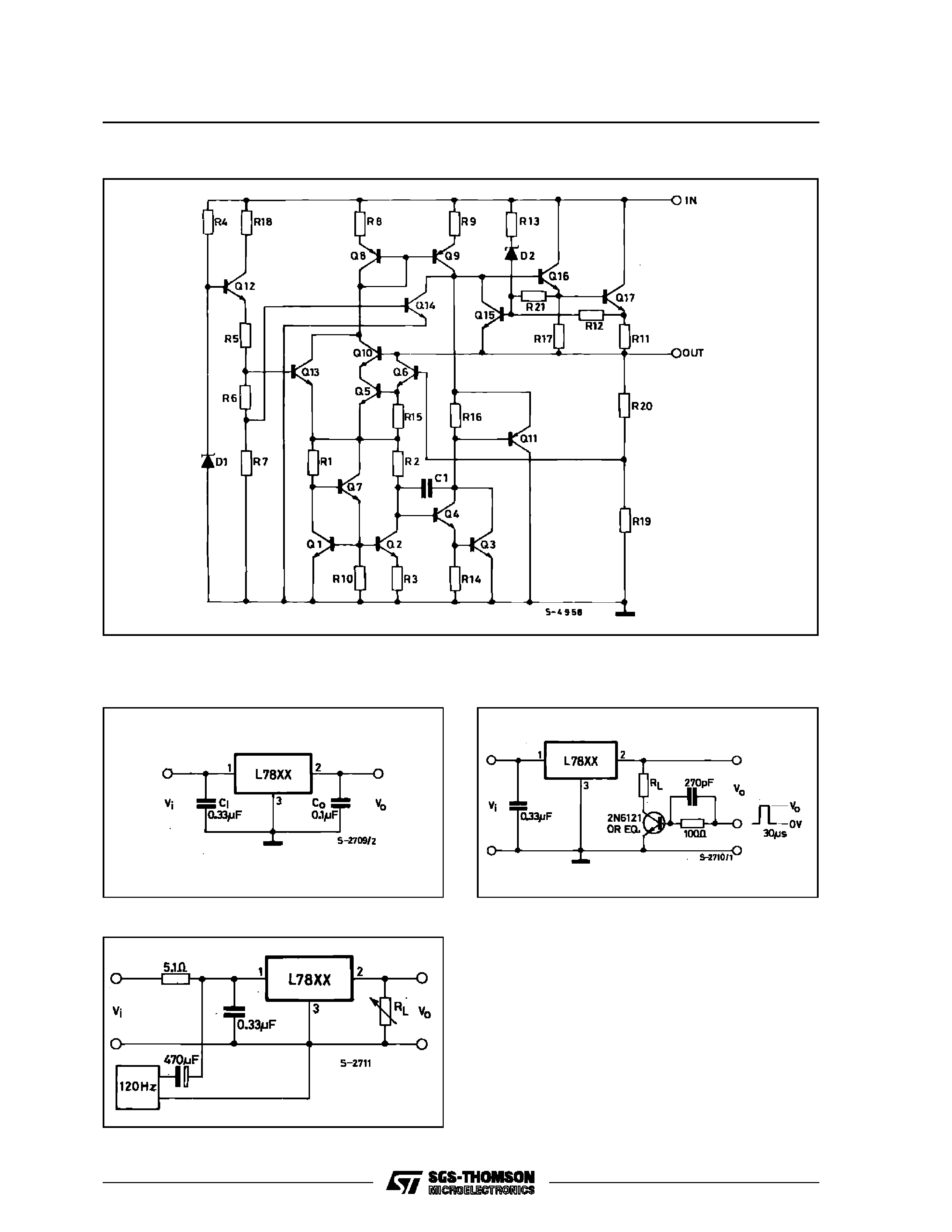
SCHEMATIC DIAGRAM
TEST CIRCUITS
Figure 1 : DC Parameters.
Figure 2 : Load Regulation.
Figure 3 : Ripple Rejection.
L7800AB/AC SERIES
3/14
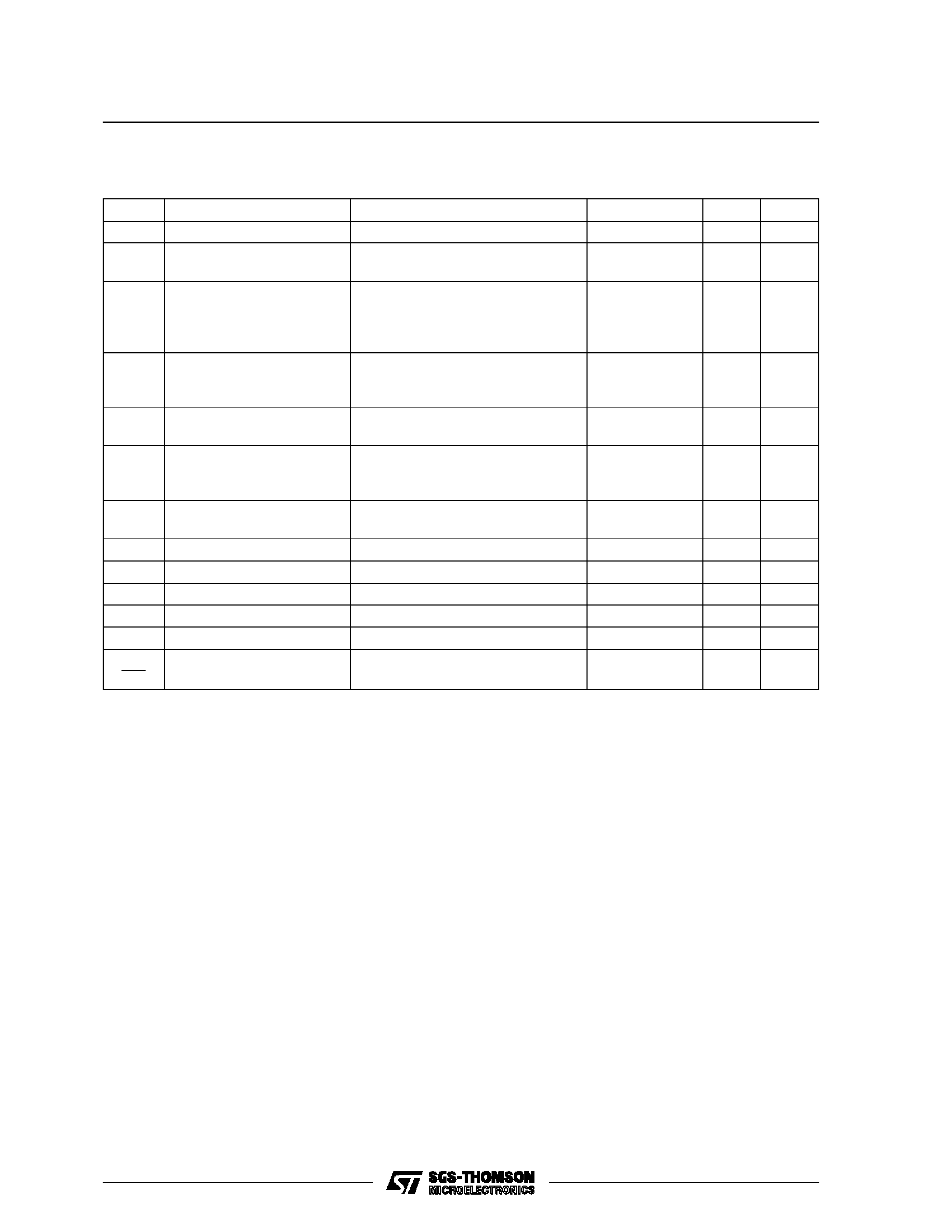
ELECTRICAL CHARACTERISTICS FOR L7805A (Vi = 10V, Io = 1 A, Tj = 0 to 125
oC (L7805AC),
Tj = -40 to 125
oC (L7805AB) unless otherwise specified)
Symbol
Parameter
Test Conditions
Min.
Typ.
Max.
Unit
Vo
Output Voltage
Tj =25
oC
4.9
5
5.1
V
Vo
Output Voltage
Io = 5 mA to 1 A
Po
15 W
Vi = 7.5 to 20 V
4.8
5
5.2
V
Vo*
Line Regulation
Vi = 7.5 to 25 V
Io = 500 mA
Vi = 8 to 12 V
Vi = 8 to 12 V
Tj =25
oC
Vi = 7.3 to 20 V
Tj =25
oC
7
10
2
7
50
5
25
50
mV
mV
mV
mV
Vo*
Load Regulation
Io = 5 mA to 1 A
Io = 5 mA to 1.5 A
Tj =25
oC
Io = 250 to 750 mA
25
30
8
100
100
50
mV
mV
mV
Id
Quiescent Current
Tj =25
oC
4.3
6
6
mA
Id
Quiescent Current Change
Vi = 8 to 25 V
Io = 500 mA
Vi = 7.5 to 20 V
Tj =25
oC
Io = 5 mA to 1 A
0.8
0.8
0.5
mA
mA
mA
SVR
Supply Voltage Rejection
Vi = 8 to 18 V
f = 120 Hz
Io = 500 mA
68
dB
Vd
Dropout Voltage
Io =1 A
Tj =25
oC2
V
eN
Output Noise Voltage
B = 10Hz to 100KHz
Tj =25
oC10
µV/Vo
Ro
Output Resistance
f = 1KHz
17
m
Isc
Short Circuit Current
Vi =35 V
Tamb =25
oC
0.2
A
Iscp
Short Circuit Peack Current
Tj =25
oC
2.2
A
Vo
T
Output Voltage Drift
-1.1
mV/
oC
* Load and line regulation are specified at constant junction temperature. Changes in Vo due to heating effects must be taken into account
separately. Pulse testing with low duty cycle is used.
L7800AB/AC SERIES
4/14

* Load and line regulation are specified at constant junction temperature. Changes in Vo due to heating effects must be taken into account
separately. Pulse testing with low duty cycle is used.
ELECTRICAL CHARACTERISTICS FOR L7806A (Vi = 11V, Io = 1 A, Tj = 0 to 125
oC (L7806AC),
Tj = -40 to 125
oC (L7806AB) unless otherwise specified)
Symbol
Parameter
Test Conditions
Min.
Typ.
Max.
Unit
Vo
Output Voltage
Tj =25
oC
5.88
6
6.12
V
Vo
Output Voltage
Io = 5 mA to 1 A
Po
15 W
Vi = 8.6 to 21 V
5.76
6
6.24
V
Vo*
Line Regulation
Vi = 8.6 to 25 V
Io = 500 mA
Vi = 9 to 13 V
Vi = 9 to 13 V
Tj =25
oC
Vi = 8.3 to 21 V
Tj =25
oC
9
11
3
9
60
60
30
60
mV
mV
mV
mV
Vo*
Load Regulation
Io = 5 mA to 1 A
Io = 5 mA to 1.5 A
Tj =25
oC
Io = 250 to 750 mA
25
30
10
100
100
50
mV
mV
mV
Id
Quiescent Current
Tj =25
oC
4.3
6
6
mA
Id
Quiescent Current Change
Vi = 9 to 25 V
Io = 500 mA
Vi = 8.6 to 21 V
Tj =25
oC
Io = 5 mA to 1 A
0.8
0.8
0.5
mA
mA
mA
SVR
Supply Voltage Rejection
Vi = 9 to 19 V
f = 120 Hz
Io = 500 mA
65
dB
Vd
Dropout Voltage
Io =1 A
Tj =25
oC2
V
eN
Output Noise Voltage
B = 10Hz to 100KHz
Tj =25
oC10
µV/Vo
Ro
Output Resistance
f = 1KHz
17
m
Isc
Short Circuit Current
Vi =35 V
Tamb =25
oC
0.2
A
Iscp
Short Circuit Peack Current
Tj =25
oC
2.2
A
Vo
T
Output Voltage Drift
-0.8
mV/
oC
L7800AB/AC SERIES
5/14