L4904A
DUAL 5V REGULATOR WITH RESET
July1993
PRELIMINARY DATA
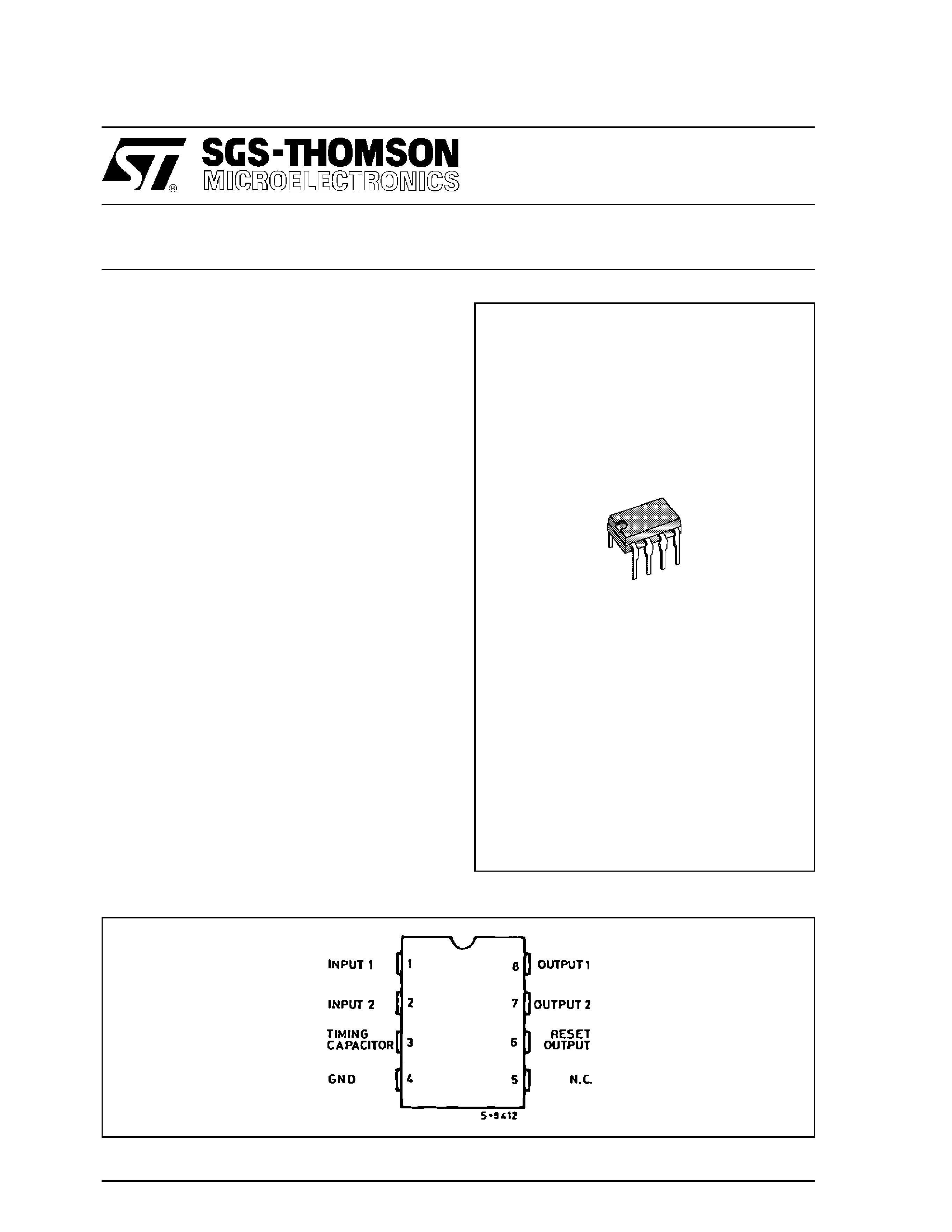
PIN CONNECTION
Minidip
ORDERING NUMBER : L4904A
.
OUTPUT CURRENTS : I01 = 50mA
I02 = 100mA
.
FIXED PRECISION OUTPUT VOLTAGE
5V
± 2%
.
RESET FUNCTION CONTROLLED BY INPUT
VOLTAGE AND OUTPUT 1 VOLTAGE
.
RESET
FUNCTION
EXTERNALLY
PRO-
GRAMMABLE TIMING
.
RESET OUTPUT LEVEL RELATED TO
OUTPUT 2
.
OUTPUT 2 INTERNALLY SWITCHED WITH
ACTIVE DISCHARGING
.
LOW LEAKAGE CURRENT, LESS THAN 1
µA
AT OUTPUT 1
.
LOW QUIESCENT CURRENT (Input 1)
.
INPUT OVERVOLTAGE PROTECTION UP TO
60V
.
RESET OUTPUT NORMALLY HIGH
.
OUTPUT TRANSISTORS SOA PROTECTION
.
SHORT CIRCUIT AND THERMAL OVER-
LOAD PROTECTION
DESCRIPTION
The L4904A is a monolithic low drop dual 5V regu-
lator designed mainly for supplying microprocessor
systems.
Reset and data save functions during switch on/off
can be realized.
1/9
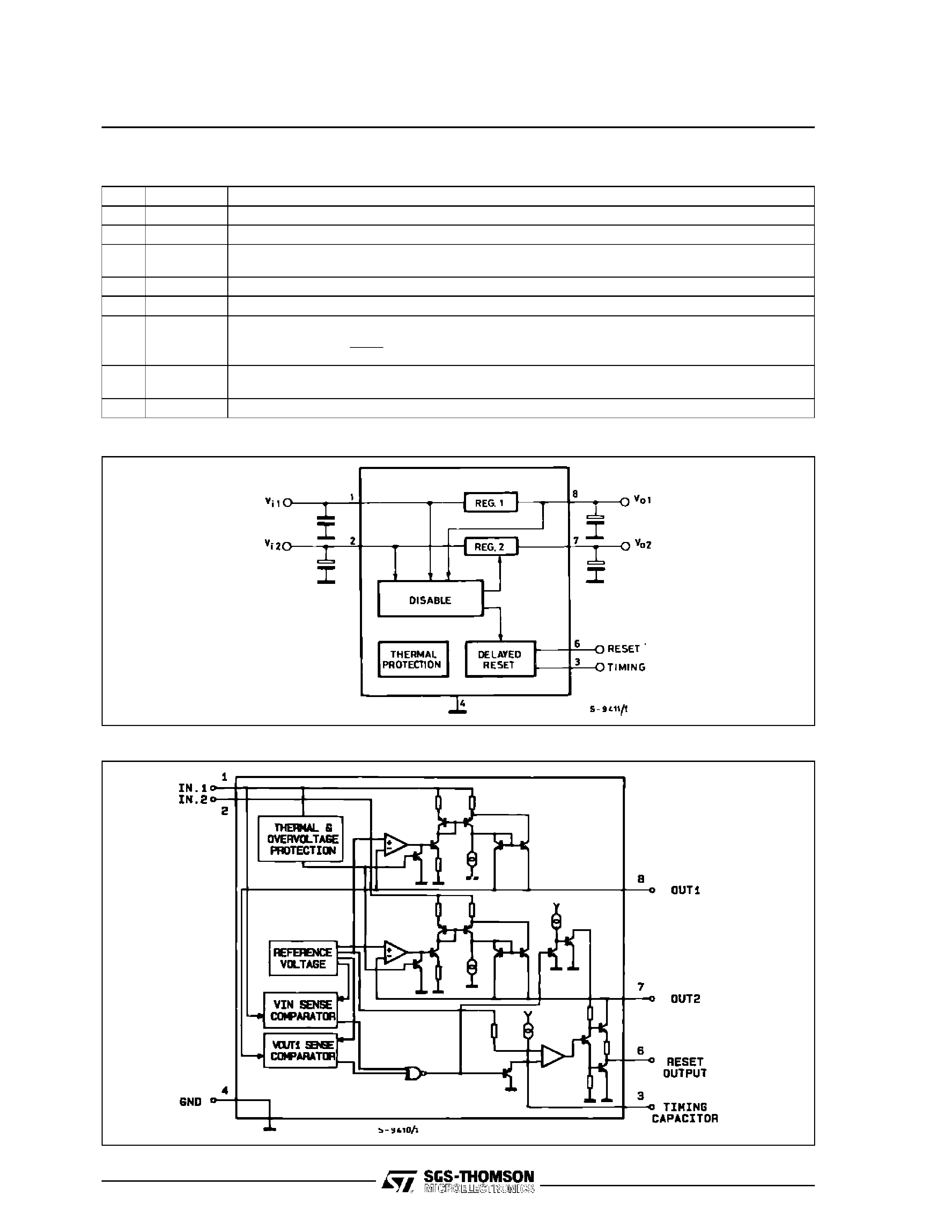
BLOCK DIAGRAM
SCHEMATIC DIAGRAM
PIN FUNCTIONS
N
°
Name
Function
1
Input 1
Low Quiescent Current 50mA Regulator Input.
2
Input 2
100mA Regulator Input.
3
Timing
Capacitor
If Reg. 2 is switching-ON the delay capacitor is charged with a 10
µA constant current. When
Reg. 2 is switched-OFF the delay capacitor is discharged.
4
GND
Common Ground.
5
N.C.
Not connected.
6
Reset
Output
When pin 3 reaches 5V the reset output is switched high.
Therefore tRD =Ct (
5V
10
µA
); tRD (ms) = Ct (nF).
7
Output 2
5V 100mA Regulator Output. Enabled if Vo 1> VRT and VIN 2 >VIT. If Reg. 2 is switched-OFF
the Co2 capacitor is discharged.
8
Output 1
5V 50mA regulator output with low leakage in switch-OFF condition.
L4904A
2/9
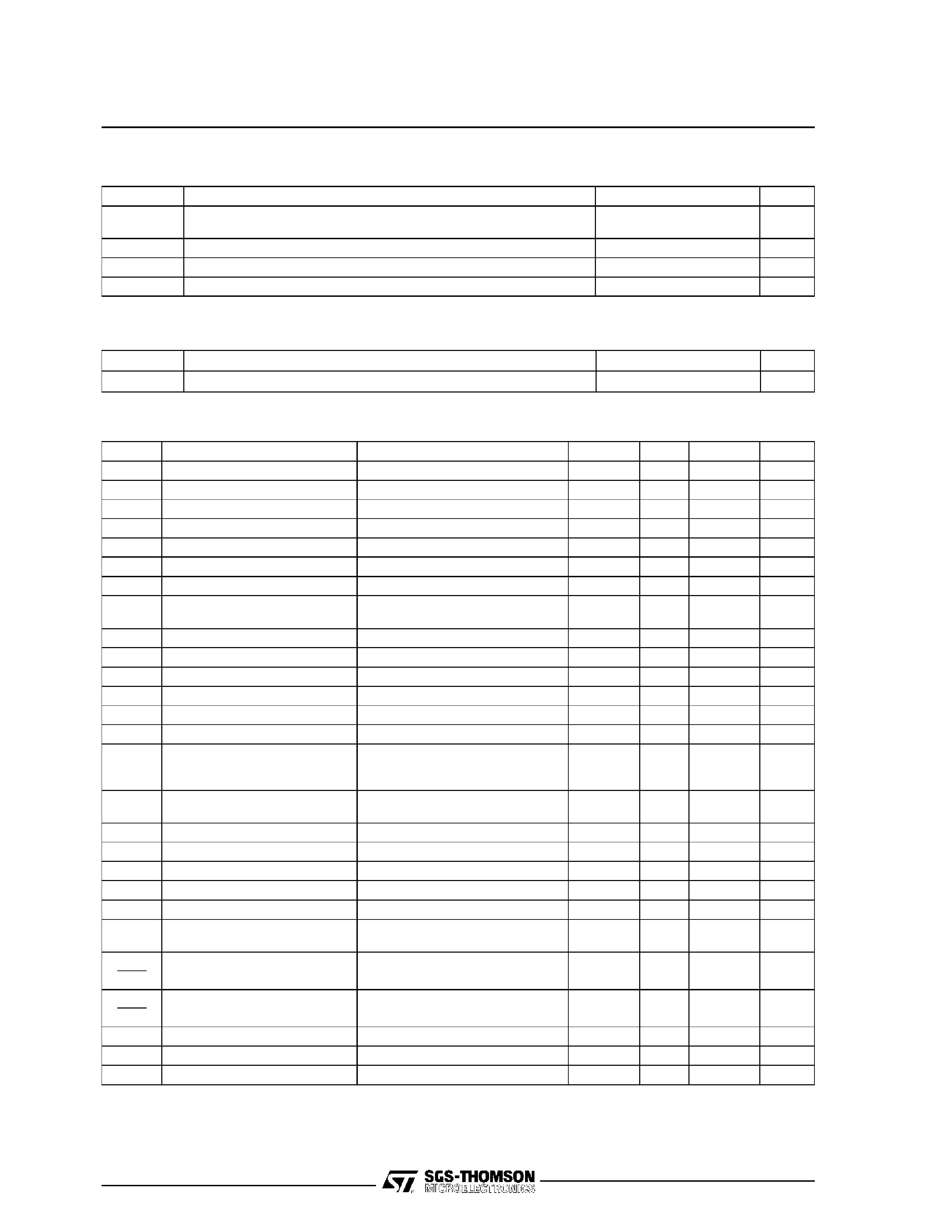
ABSOLUTE MAXIMUM RATINGS
Symbol
Parameter
Value
Unit
VIN
DC Input Voltage
Transient Input Overvoltage (t = 40ms)
24
60
V
V
Io
Output Current
Internally Limited
Ptot
Power Dissipation at Tamb =50
°C1
W
Tj
Storage and Junction Temperature
40 to 150
°C
THERMAL DATA
Symbol
Parameter
Value
Unit
Rth j-amb
Thermal Resistance Junction-ambient
Max
100
°C/W
ELECTRICAL CHARACTERISTICS (VIN = 14.4V, Tamb =25
oC unless otherwise specified)
Symbol
Parameter
Test Conditions
Min.
Typ.
Max.
Unit
Vi
DC Operating Input Voltage
20
V
V01
Output Voltage 1
R Load 1k
4.95
5.05
5.15
V
V02 H
Output Voltage 2 HIGH
R Load 1k
V01 0.1
5
V01
V
V02 L
Output Voltage 2 LOW
I02 = 5mA
0.1
V
I01
Output Current 1
V01 = 100mV
50
mA
IL01
Leakage Output 1 Current
VIN =0, V01
3V
1
µA
I02
Output Current 2
V02 = 100mV
100
mA
VI01
Output 1 Dropout Voltage (*)
I01 = 10mA
I01 = 50mA
0.7
0.75
0.8
0.9
V
V
VIT
Input Threshold Voltage
V01 + 1.2
6.4
V01 + 1.7
V
VITH
Input Threshold Voltage Hyst.
250
mV
V01
Line Regulation
7V < VIN < 18V, I01 = 5mA
5
50
mV
V02
Line Regulation 2
7V < VIN < 18V, I02 = 5mA
5
50
mV
V01
Load Regulation 1
VIN = 8V, 5mA < I01 < 50mA
5
20
mV
V02
Load Regulation 2
VIN = 8V, 5mA < I02 < 100mA
10
50
mV
IQ
Quiescent Current
I02 =I01
5mA
0< VIN < 13V
7V < VIN < 13V
4.5
1.6
6.5
3.5
mA
IQ1
Quiescent Current 1
6.3V < VIN1 < 13V, VIN2 =0
I01
5mA, I02 =0
0.6
0.9
mA
VRT
Reset Threshold Voltage
V02 0.15
4.9
V02 0.05
V
VRTH
Reset Threshold Hysteresis
30
50
80
mV
VRH
Reset Output Voltage HIGH
IR = 500
µAV02 1
4.12
V02
V
VRL
Reset Output Voltage LOW
IR = 5mA
0.25
0.4
V
tRD
Reset Pulse Delay
Ct = 10nF
3
11
ms
td
Timing Capacitor Discharge
Time
Ct = 10nF
20
µs
V01
T
Thermal Drift
20
°C <0>Tamb 125°C
0.3
0.8
mV/
°C
V02
T
Thermal Drift
20
°C <0>Tamb 125°C
0.3
0.8
mV/
°C
SVR1
Supply Voltage Rejection
f = 100Hz, VR = 0.5V, Io = 50mA
50
84
dB
SVR2
Supply Voltage Rejection
f = 100Hz, VR = 0.5V, Io = 100mA
50
80
dB
TJSD
Thermal Shut Down
150
°C
* The dropout voltage is defined as the difference between the input and the output voltage when the output voltage is lowered of 25 mV under
constant output current condition.
L4904A
3/9
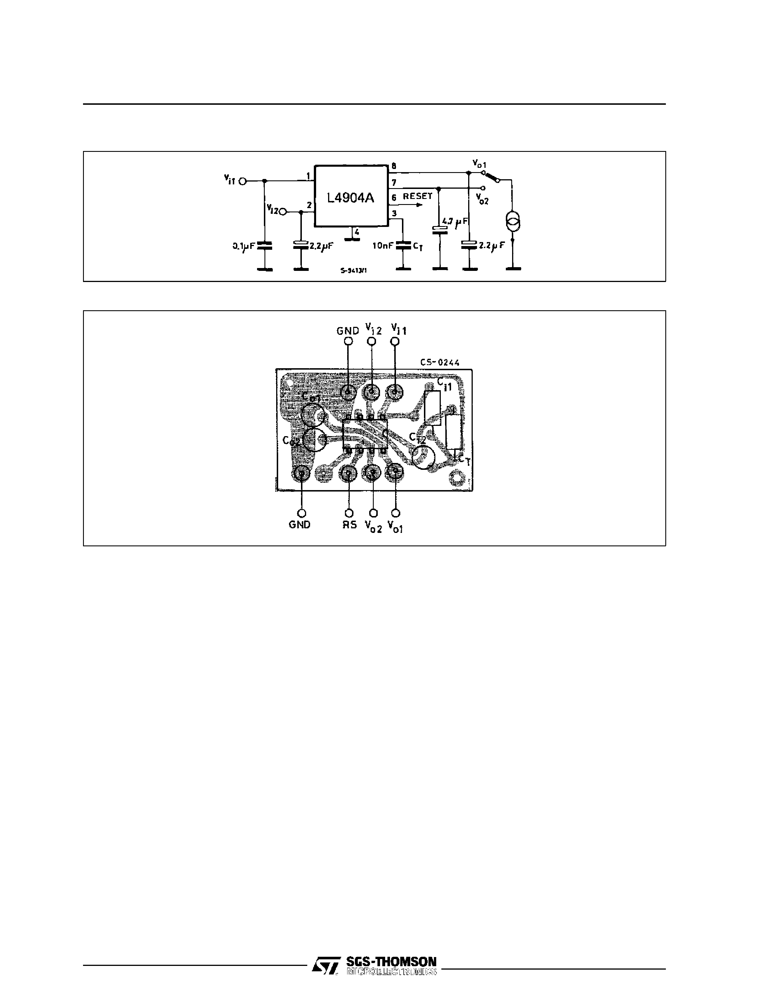
TEST CIRCUIT
Figure 1 : P.C. Board and Components Layout of the Test Circuit (1:1 scale)
APPLICATION INFORMATION
In power supplies for
µP systems it is necessary to
provide power continuously to avoid loss of infor-
mation in memories and in time of day clocks, or to
save data when the primary supply is removed. The
L4904A makes it very easy to supply such equip-
ments ; it provides two voltage regulators (booth 5V
high precision) with separate inputs plus a reset
output for the data save function.
CIRCUIT OPERATION (see Figure 2)
After switch on Reg. 1 saturates until V01 rises to
the nominal value.
When the input 2 reaches VIT and the output 1 is
higher than VRT the output 2 (V02) switches on and
the reset output (VR) also goes high after a pro-
grammable time TRD (timing capacitor).
V02 and VR are switched together at low level when
one of the following conditions occurs :
- an input overvoltage
- an overload on the output 1 (V01 <VRT);
- a switch off (VIN <VIT -VITH);
and they start again as before when the condition
is removed.
An overload on output 2 does not switch Reg. 2,
and does not influence Reg. 1.
The V01 output features :
- 5 V internal reference without voltage divider
between the output and the error comparator ;
- very low drop series regulator element utilizing
mirrors ;
permit high output impedance and then very low
leakage current even in power down conditions.
This output may thereforebe used to supply circuits
continuously, such as volatile RAMs, allowing the
use of a back-up battery. The V01 regulator also
features low consumption (0.6 mA typ.) to minimize
battery drain in applications where the V1 regulator
is permanently connected to a battery supply.
The V02 output can supply other non essential 5 V
circuits which may be powered down when the
system is inactive, or that must be powered down
to prevent uncorrect operation for supply voltages
below the minimum value.
The reset output can be used as a "POWER DOWN
INTERRUPT", permitting RAM access only in cor-
rect power conditions, or as a "BACK-UP ENABLE"
to transfer data into in a NV SHADOW MEMORY
when the supply is interrupted.
L4904A
4/9
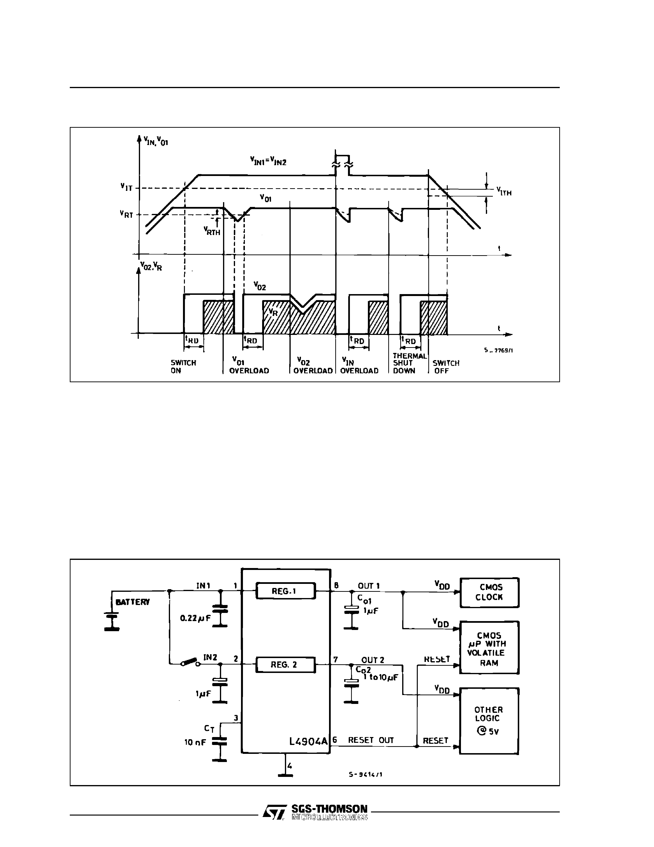
Figure 2
APPLICATION SUGGESTIONS
Figure 3 shows an application circuit for a
µP
system.
Reg. 1 is permanently connected to a battery and
supplies a CMOS time-of-day clock and a CMOS
microcomputer chip with volatile memory.
Reg. 2 may be switched OFF when the system is
inactive.
Figure 4 shows the L4904A with a back up battery
on the V01 output to maintain a CMOS time-of-day
clock and a stand by type C-MOS
µP. The reset
output makes sure that the RAM is forced into the
low consumption stand by state, so the access to
memory is inhibit and the back up battery voltage
cannot drop so low that memory contents are cor-
rupted.
In this case the main on-off switch disconnectsboth
regulators from the supply battery.
Application Circuits of a Microprocessor system
(Figure 3) or with data save battery (Figure 4). The
reset output provide delayed rising front at the
turn-off of the regulator 2.
Figure 3
L4904A
5/9