LOW POWER DUAL OPERATIONAL AMPLIFIERS
.
INTERNALLY FREQUENCY COMPENSATED
.
LARGE DC VOLTAGE GAIN : 100dB
.
WIDE BANDWIDTH (unity gain) : 1.1MHz
(temperature compensated)
.
VERY
LOW
SUPPLY
CURRENT/AMPLI
(500
µA) - ESSENTIALLY INDEPENDENT OF
SUPPLY VOLTAGE
.
LOW INPUT BIAS CURRENT : 20nA
(temperature compensated)
.
LOW INPUT OFFSET VOLTAGE : 2mV
.
LOW INPUT OFFSET CURRENT : 2nA
.
INPUT COMMON-MODE VOLTAGE RANGE
INCLUDES GROUND
.
DIFFERENTIAL INPUT VOLTAGE RANGE
EQUAL TO THE POWER SUPPLY VOLTAGE
.
LARGE OUTPUT VOLTAGE SWING 0V TO
(VCC 1.5V)
DESCRIPTION
These circuits consist of two independent,high gain,
internally frequency compensated which were
designed specifically to operate from a single power
supply over a wide range of voltages. The low power
supply drain is independent of the magnitude of the
power supply voltage.
Application areas include transducer amplifiers, dc
gain blocks and all the conventional op-amp circuits
which now can be more easilyimplemented in single
power supply systems. For example, these circuits
can be directly operatedoff the standard+ 5V power
supply voltage which is used in logic systems and
will easily provide the required interface electronics
without requiring any additional power supply.
In the linear mode the input common-mode voltage
range includes ground and the output voltage can
also swing to ground, even though operated from
only a single power supply voltage.
The
gain-bandwidth
product
is
temperature
compensated.
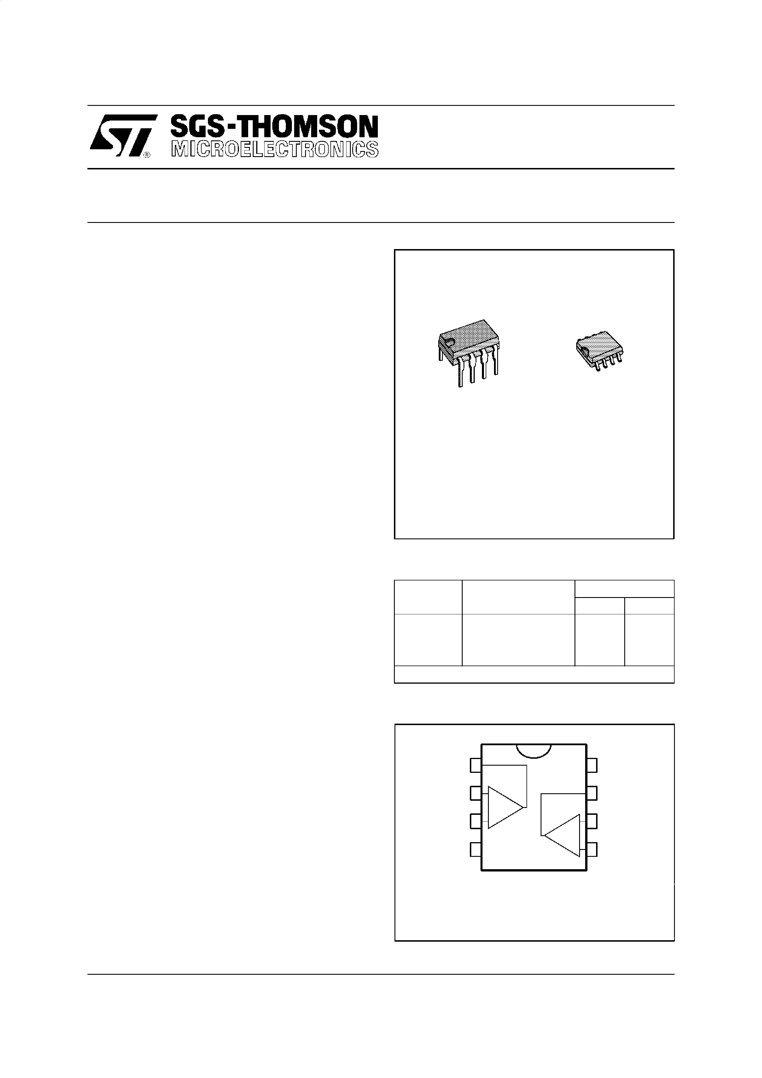
N
DIP8
(Plastic Package)
ORDER CODES
Part
Number
Temperature
Range
Package
ND
LM158,A
55
oC, +125oC
··
LM258,A
40
oC, +105oC
··
LM358,A
0
oC, +70oC
··
Example : LM258N
158-01.TBL
D
SO8
(Plastic Micropackage)
LM158,A-LM258,A
LM358,A
October 1994
1
2
3
45
6
7
8
-
+
-
+
1 - Output 1
2 - Inverting input 1
3 - Non-inverting input 1
4- VCC
-
5 - Non-inverting input 2
6 - Inverting input 2
7 - Ouput 2
8- VCC
+
PIN CONNECTIONS (top view)
1/11
ABSOLUTE MAXIMUM RATINGS
Symbol
Parameter
LM158,A
LM258,A
LM358,A
Unit
VCC
Supply Voltage
+32
+32
+32
V
Vi
Input Voltage
0.3 to +32
0.3 to +32
0.3 to +32
V
Vid
Differential Input Voltage
+32
+32
+32
V
Output Short-circuit Duration - (note 2)
Infinite
Ptot
Power Dissipation
500
500
500
mW
Iin
Input Current - (note 1)
50
50
50
mA
Toper
Operating Free-air Temperature Range
55 to +125
40 to +105
0 to +70
oC
Tstg
Storage Temperature Range
65 to +150
65 to +150
65 to +150
oC
158-02.TBL
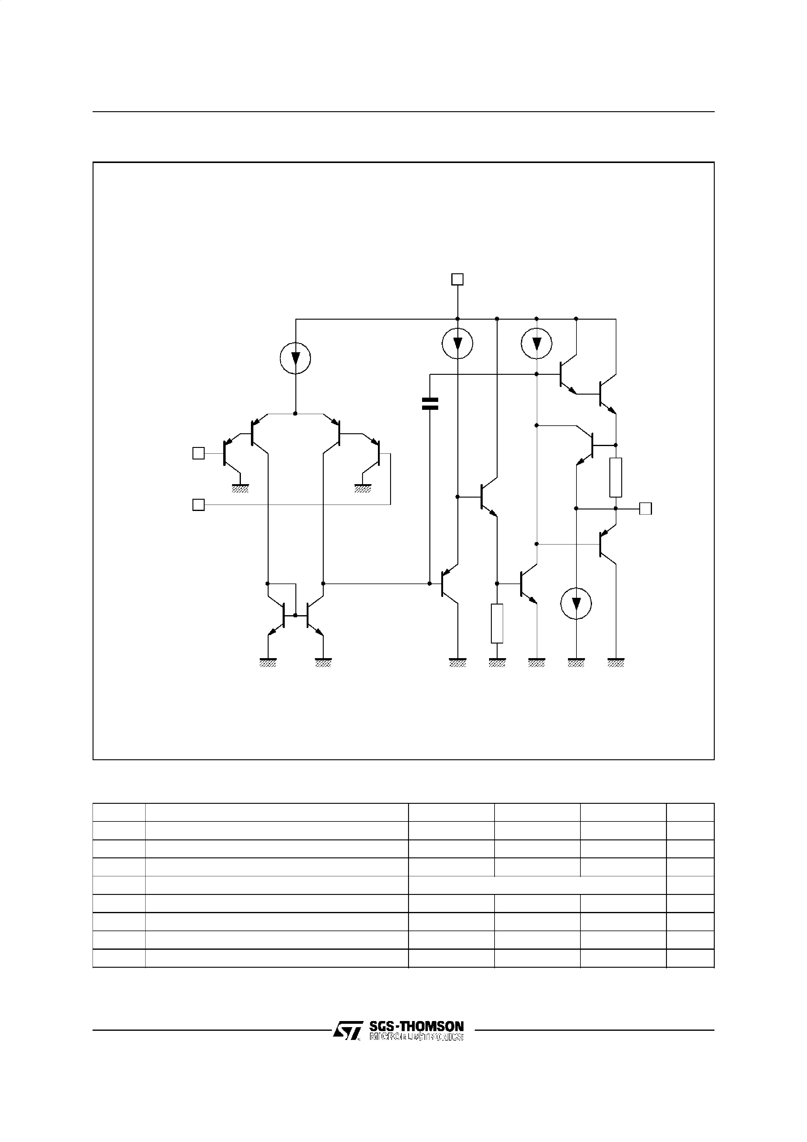
6
µA
4
µA
100
µA
Q2
Q3
Q4
Q1
Inverting
input
Non-inverting
input
Q8
Q9
Q10
Q11
Q12
50
µA
Q13
Output
Q7
Q6
Q5
R
SC
V
CC
C C
GND
158-02.EPS
SCHEMATIC DIAGRAM (1/2 LM158)
LM158,A - LM258,A - LM358,A
2/11
ELECTRICAL CHARACTERISTICS
VCC
+ = +5V, VCC = Ground, VO = 1.4V, Tamb =25oC (unless otherwise specified)
Symbol
Parameter
LM158A
LM258A
LM358A
LM158
LM258
LM358
Unit
Min.
Typ.
Max.
Min.
Typ.
Max.
Vio
Input Offset Voltage - (note 3)
Tamb =25
oC
LM158, LM258
LM158A
Tmin.
Tamb Tmax.
LM158, LM258
13
2
4
27
5
9
7
mV
Iio
Input Offset Current
Tamb =25
oC
Tmin.
Tamb Tmax.
210
30
230
40
nA
Iib
Input Bias Current - (note 4)
Tamb =25
oC
Tmin.
Tamb Tmax.
20
50
100
20
150
200
nA
Avd
Large Signal Voltage Gain
(VCC = +15V, RL =2k
,VO = 1.4V to 11.4V)
Tamb =25
oC
Tmin.
Tamb Tmax.
50
25
100
50
25
100
V/mV
SVR
Supply Voltage Rejection Ratio (RS = 10k
)
(VCC
+ = 5 to 30V)
Tamb =25
oC
Tmin.
Tamb Tmax.
65
65
100
65
65
100
dB
ICC
Supply Current, all Amp, no Load
VCC = +5V, Tmin.
Tamb Tmax.
VCC = +30V, Tmin.
Tamb Tmax.
0.7
1.2
2
0.7
1.2
2
mA
Vicm
Input Common Mode Voltage Range
(VCC = +30V) - (note 6)
Tamb =25
oC
Tmin.
Tamb Tmax.
0
0
VCC
+1.5
VCC
+2
0
0
VCC
+1.5
VCC
+2
V
CMR
Common-mode Rejection Ratio (RS = 10k
)
Tamb =25
oC
Tmin.
Tamb Tmax.
70
60
85
70
60
85
dB
IO
Output Short Circuit Current
(VCC = +15V, Vo = 2V, Vid = +1V)
20
40
60
20
40
60
mA
Isink
Output Current Sink (Vid = -1V)
VCC = +15V, VO =2V
VCC = +15V, VO = +0.2V
10
12
20
50
10
12
20
50
mA
µA
VOPP
Output Voltage Swing (RL =2k
)
Tamb =25
oC
Tmin.
Tamb Tmax.
0
0
VCC
+1.5
VCC
+2
0
0
VCC
+1.5
VCC
+2
V
VOH
High Level Output Voltage (VCC
+ = 30V)
Tamb =25
oCRL =2k
Tmin.
Tamb Tmax.
Tamb =25
oCRL = 10k
Tmin.
Tamb Tmax.
26
26
27
27
27
28
26
26
27
27
27
28
V
VOL
Low Level Output Voltage (RL = 10k
)
Tamb =25
oC
Tmin.
Tamb Tmax.
520
20
520
20
mV
SR
Slew Rate (VCC = 15V, VI = 0.5 to 3V, RL =
2k
,CL = 100pF, Tamb =25oC, unity gain)
0.3
0.6
0.3
0.6
V/
µs
GBP
Gain Bandwidth Product
(VCC = 30V, f = 100kHz, Tamb =25
oC,
Vin = 10mV, RL =2k
,CL = 100pF)
0.7
1.1
0.7
1.1
MHz
THD
Total Harmonic Distortion
(f = 1kHz, Av = 20dB, RL =2k
,VCC = 30V,
CL = 100pF, Tamb =25
oC, VO =2 PP)
0.02
0.02
%
en
Equivalent Input Noise voltage
(f = 1kHz, Rs = 100
,VCC = 30V)
55
55
nV
Hz
158-03.TBL
LM158,A - LM258,A - LM358,A
3/11
ELECTRICAL CHARACTERISTICS (continued)
Symbol
Parameter
LM158A
LM258A
LM358A
LM158
LM258
LM358
Unit
Min.
Typ.
Max.
Min.
Typ.
Max.
DVio
Input Offset Voltage Drift
7
15
7
30
µV/oC
DIio
Input Offset Current Drift
10
200
10
300
pA/
oC
VO1/VO2
Channel Separation (note 5)
1kHz
f 20kHz
120
120
dB
Notes :
1. This input current only exist when the voltage at any of the input leads is driven negative. It is due to the collec-
tor-base junction of the input PNP transistor becoming forward biased and thereby acting as input diode clamps.
In addition to this diode action, there is also NPN parasiti c action on the IC chip. This transistor action can cause
the output voltages of the Op-amps to go to the VCC voltage level (or to ground for a large overdrive) for the time
duration that an input is driven negative.
This is not destructive and normal output will set up again for input voltage higher than 0.3V.
2. Short-circuits from the output to VCC can cause excessive heating if VCC
+ > 15V. The maximum output current is
approximatively 40mA independent of the magnitude of VCC. Destructive dissipation can result from simultaneous
short-circuits on all amplifi ers.
3. VO
= 1.4V, RS =0,5V < VCC+ < 30V, 0 < Vic < VCC+ 1.5V.
4. The direction of the input current is out of the IC. This current is essentially constant, independent of the state of
the output so no loading change exists on the input lines.
5. Due to the proximity of external components insure that coupling is not originating via stray capacitance between
these external parts. This typically can be detected as this type of capacitance increases at higher frequences.
6. The input common-mode voltage of either input signal voltage should not be allowed to go negative by more than
0.3V. The upper end of the common-mode voltage range is VCC
+ 1.5V.
But either or both inputs can go to +32V without damage.
158-04.TBL
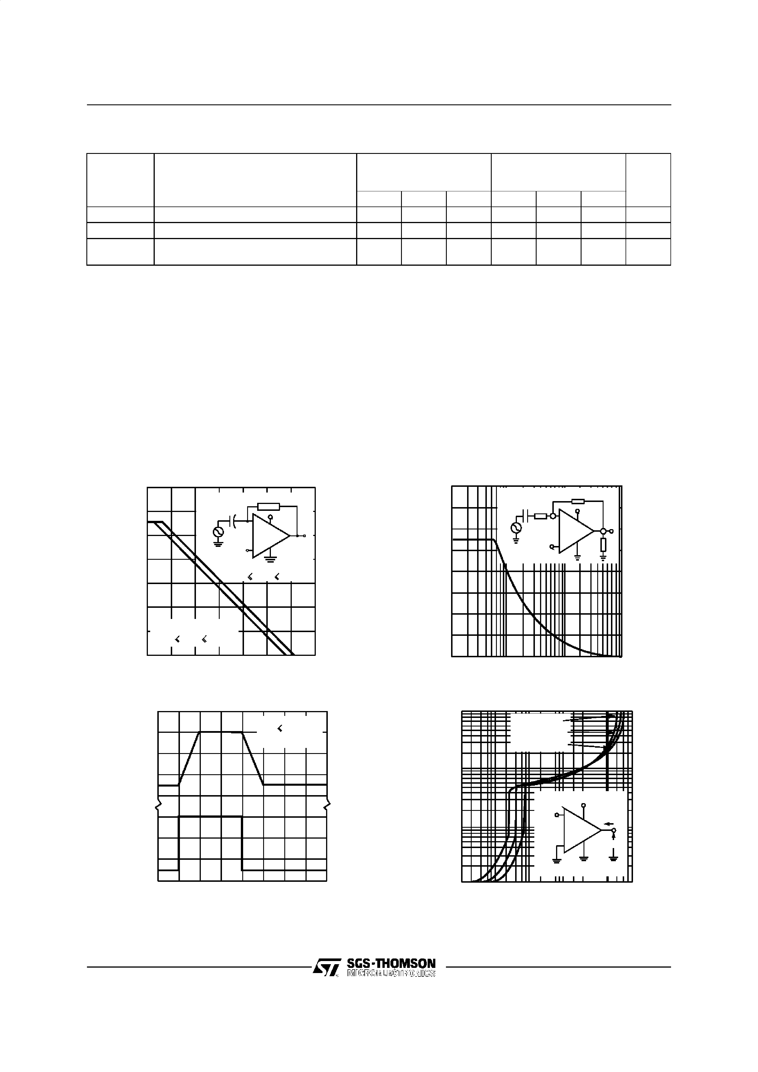
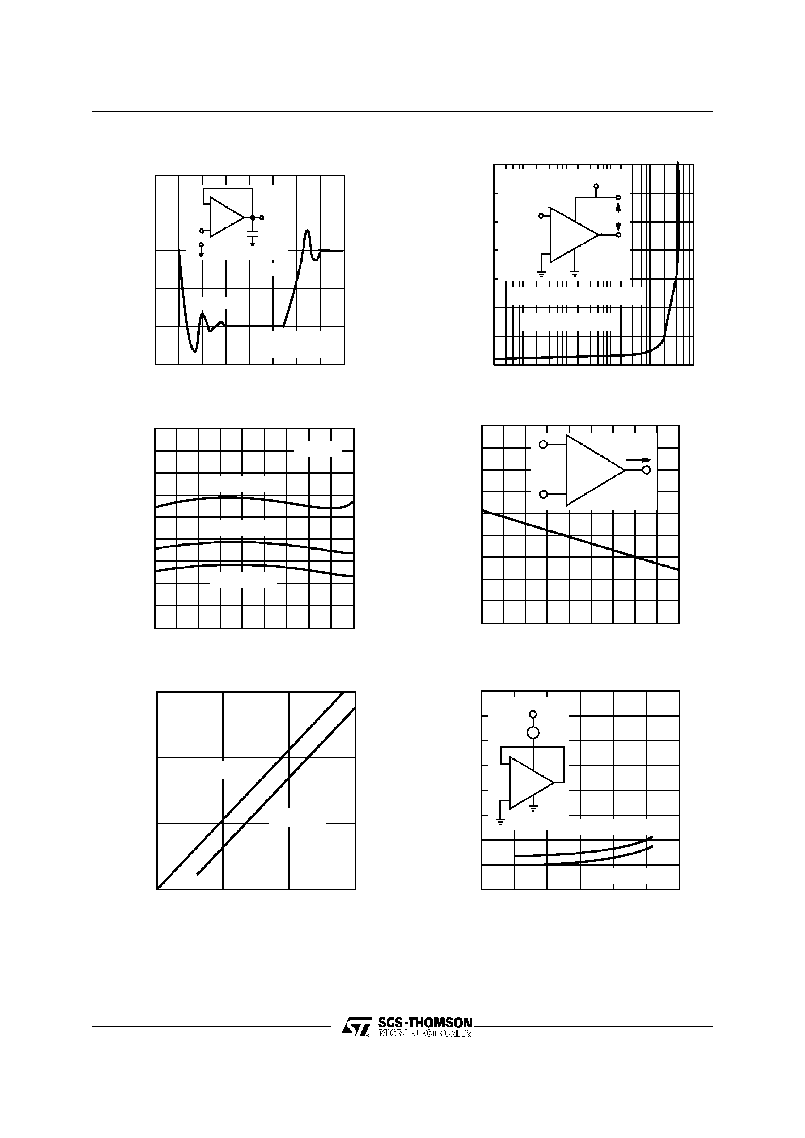
VOLTAGE
GAIN
(dB)
OP EN LOOP FREQUE NCY RES P ONS E (NOTE 3 )
1.0
10
100
1k
10k
100k
1M
10M
VCC = +10 to + 15V &
FREQ UENCY (Hz)
10M
VI
VCC/2
VCC = 30V &
0.1
µF
VCC
VO
-
+
-55 C
Tamb
+125 C
140
120
100
80
60
40
20
0
-55 C
Tamb
+125 C
INPUT
VOLTAGE
(V)
OUTPUT
VOLTAGE
(V)
VOLAGE FOLLOWER P ULSE RES P ONS E
010
20
30
40
TIME (
µs)
RL
2 k
VCC = +15V
4
3
2
1
0
3
2
1
LARG E SIGNAL FR EQUENCY RES P ONS E
FREQUENC Y (Hz)
1k
10k
100k
1M
OUTPUT
SWING
(Vpp)
+7V
2k
1k
100k
+15V
VO
-
+
VI
20
15
10
5
0
OUTPUT C HARACTERISTICS
O UTP UT S INK C URRENT (mA)
0,001
0,01
0,1
1
10
100
OUTPUT
VOLTAGE
(V)
VCC = +5V
VCC = +15V
VCC = +30V
-
IO
VO
Tamb =+25 C
vcc/2
vcc
+
10
1
0.1
0.01
LM158,A - LM258,A - LM358,A
4/11
OUTPUT
VOLTAGE
REFERENCED
TO
V
CC
+
(V)
O UTP UT CHARACTE RISTICS
0,01
0,1
1
10
100
0,00 1
Inde pe nde nt of VCC
T amb =+25 C
+
-
VCC
VO
IO
VCC /2
O UTP UT S OURCE CURRENT (mA)
8
7
6
5
4
3
2
1
OUTPUT
VOLTAGE
(mV)
VOLTAGE FO LLOWER P ULS S E RES P ONS E
(S MALL S IGNAL)
0
123
45678
Input
Tamb =+25 C
VCC =30 V
Ou tput
e O
e l
50pF
+
-
TIME (
µs)
500
450
400
350
300
250
INPUT
CURRENT
(mA)
INPUT CURRENT (No te 1)
-55
-35
-15
5
25
45
65
85
105
125
VI =0 V
VCC =+30 V
VCC =+15 V
VCC =+5 V
TEMPERATURE ( C)
90
80
70
60
50
40
30
20
10
0
OUTPUT
CURRENT
(mA)
CURRENT LIMITING (Note 1)
-
+
IO
TE MPE RATURE ( C)
90
80
70
60
50
40
30
20
10
0
-55
-35
-15
5
25
4 5
65
8 5 1 05
125
SUPPLY
CURRENT
(mA)
SUP P LY CURRE NT
010
20
30
Tamb =-55 C
VCC
mA
ID
-
+
Tamb = 0 C to +125 C
P OS ITIVE S UP P LY VOLTAGE (V)
4
3
2
1
INPUT
VOLTAGE
(V)
INP UT VOLTAGE RANGE
0
5
10
15
P OWER S UP P LY VOLTAGE (V)
NØga tive
P os itive
15
10
5
LM158,A - LM258,A - LM358,A
5/11