This is advanced information on a new product now in development or undergoing evaluation. Details are subject to change without notice.
L4938N/ND
L4938NPD
March 1995
DUAL MULTIFUNCTION VOLTAGE REGULATOR
PRELI MINARY DATA
.
STANDBY OUTPUT VOLTAGE PRECISION 5V
± 2%
.
OUTPUT 2 TRACKED TO THE STANDBY OUT-
PUT
.
OUTPUT
2
DISABLE
FUNCTION
FOR
STANDBY MODE
.
VERY LOW QUIESCENT CURRENT, LESS
THAN 250
µA, IN STANDBY MODE
.
OUTPUT 2 VOLTAGE SETTABLE FROM 5 TO
20V
.
OUTPUT CURRENTS : I01 = 50mA, I02 = 500mA
.
VERY LOW DROPOUT (max 0.4V/0.6V)
.
OPERATING TRANSIENT SUPPLY VOLTAGE
UP TO 40V
.
POWER-ON RESET CIRCUIT SENSING THE
STANDBY OUTPUT VOLTAGE
.
POWER-ON RESET DELAY PULSE DEFINED
BY THE EXTERNAL CAPACITOR
.
EARLY WARNING OUTPUT FOR SUPPLY UN-
DERVOLTAGE
.
THERMAL SHUTDOWN AND SHORT CIRCUIT
PROTECTIONS
PowerDIP
(12+2+2)
ORDERING NUMBERS: L4938N (PDIP)
L4938ND (SO)
L4938NPD (PSO20)
DESCRIPTION
The L4938N is a monolithic integrated dual voltage
regulators with two very low dropout outputsand ad-
ditional functions such as power-on reset and input
voltage sense. They are designed for supplying mi-
crocomputer controlled systems specially in auto-
motive applications.
PIN CONNECTION (top view)
SO20
(12+4+4)
N.C.
CT
EN
GND
GND
SO
RES
1
3
2
4
5
6
7VO2
GND
VO2
GND
VS2
VS1
SI
16
15
14
13
12
10
11
D95AT156
VO1
8
ADJ
9
POWERDIP
N.C.
C7
EN
GND
GND
GND
GND
RES
SO
VS1
VS2
GND
GND
GND
GND
VO2
VO2
ADJ
1
3
2
4
5
6
7
8
9
18
17
16
15
14
12
13
11
19
10
20
VO1
SI
D93AT004
SO20
PowerSO20
GND
N.C.
N.C.
V
S
VS
N.C.
SI
CT
EN
N.C.
GND
10
8
9
7
6
5
4
3
2
13
14
15
16
17
19
18
20
12
1
11
GND
D95AT169
N.C.
RESET
VO1
SO
ADJ
VO2
N.C.
GND
PowerSO20
1/12
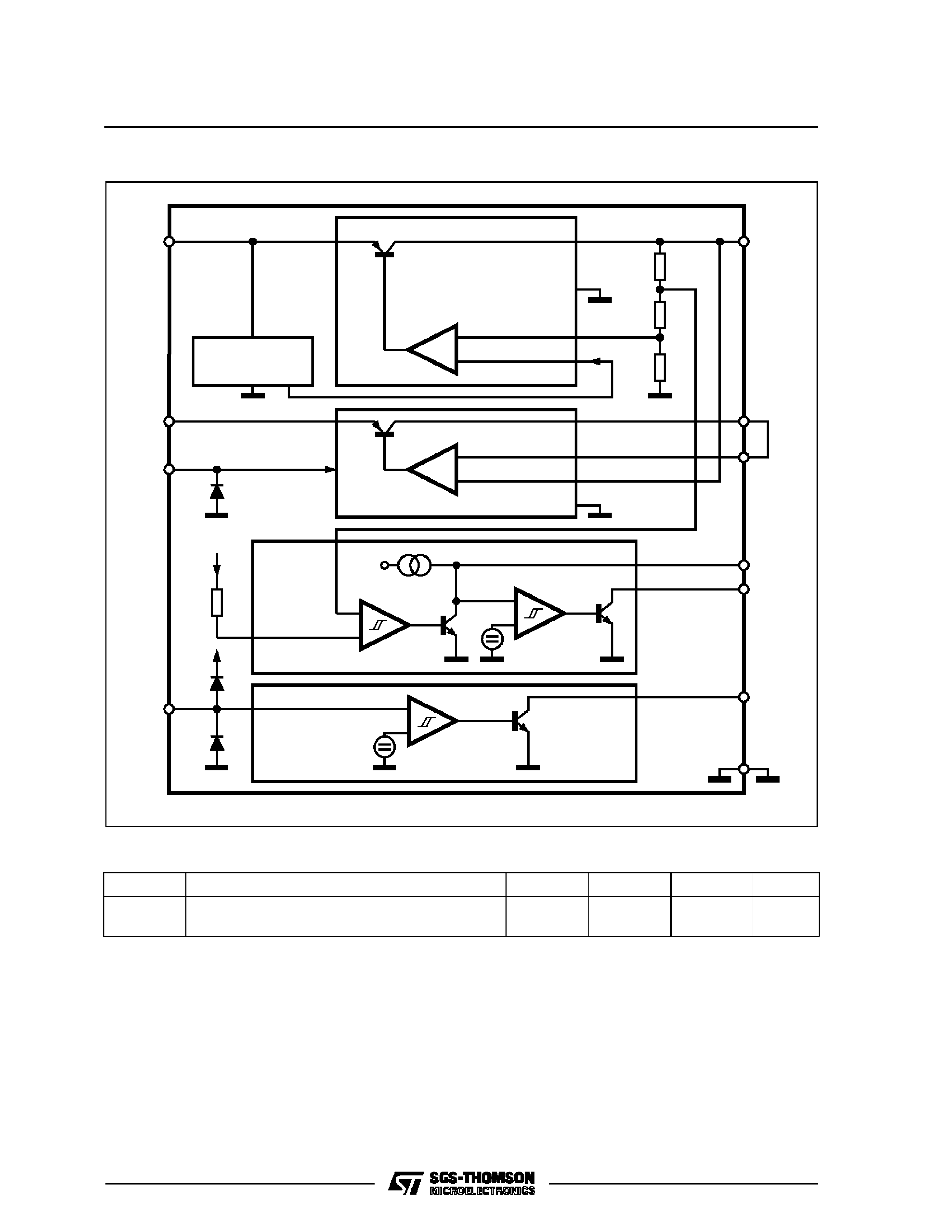
BLOCK DIAGRAM
REG1
1.23V
REFERENCE
REG2
RESET
2.0V
1.23V
1.23V
SENSE
(optional)
VS1
VS2
EN
SI
SO
RES
CT
ADJ
VO2
VO1
GND
D94AT143A
2
µ
THERMAL DATA
Symbol
Parameter
Powerdip
PowerSO20
SO20
Unit
Rthj-case
Rthj-amb
Thermal Resistance Junction-Case
Max.
Thermal Resistance Junction-Ambient
Max.
14
90
<2
20
°C/W
°C/W
L4938N - L4938ND - L4938NPD
2/12
ABSOLUTE MAXIMUM RATINGS
Symbol
Parameter
Value
Unit
VS
DC Supply Voltage
28
V
Transient Supply Voltage (T < 1s)
40
V
Tj,Tstg
Junction and Storage Temperature Range
55 to 150
°C
ISI
Sense Input Current (VSI
0.3V or VSI >VS)
±1mA
IEN
Enable Input Current (VEN
0.3V)
±1mA
VEN
Enable Input Voltage
VS
VRES,VSO
Reset and Sense Output Voltage
20
V
IRES,ISO
Reset and Sense Output Current
5
mA
PD
Power Dissipation
875
mW
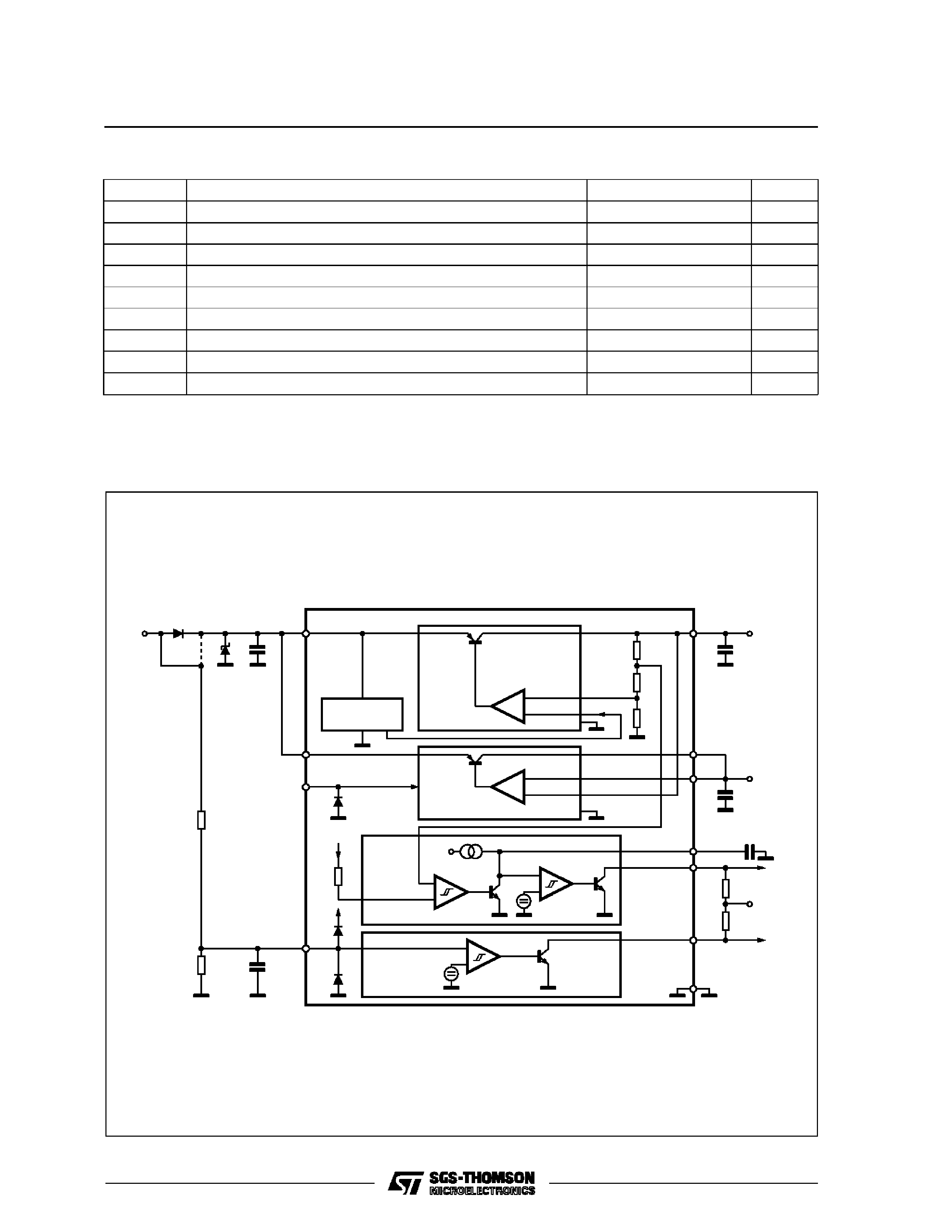
REG1
1.23V
REFERENCE
REG2
RESET
2.0V
1.23V
1.23V
SENSE
(optional)
VS1
V
S2
EN
SI
SO
RES
CT
ADJ
VO2
VO1
GND
D94AT144A
CS
CT
CO2
CO1
RRES
RSO
2
µ
VO1
APPLICATION CIRCUIT
CS
1µF; C01 6µF; C02 10µF, ESR < 10 at 10KHz
Note : The circuit is ESD protected according to MILSTD883C.
L4938N - L4938ND - L4938NPD
3/12
ELECTRICAL CHARACTERISTICS (VS = 14V; 40
°C TJ 125°C unless otherwise specified)
Symbol
Parameter
Test Conditions
Min.
Typ.
Max.
Unit
VS
Operating Supply Voltage
25
V
VO1
Standby Output Voltage
6V
VS 25V
1mA
IO1 50mA
4.90
5.00
5.10
V
VO2 -VO1
Output Voltage 2 Tracking Error
(note 1)
6V
VS 25V
5mA
IO2 500mA
Enable = LOW
25
+25
mV
IADJ
ADJ Input Current
IO1 = 1mA; IO2 = 5mA
1
0.1
1
µA
VDP1
Dropout Voltage 1
IO1 =10mA
IO1 =50mA
0.1
0.2
0.25
0.4
V
V
VIO1
Input to Output Voltage
Difference in Undervoltage
Condition
VS = 4V, IO1 = 35mA
0.4
V
VDP2
Dropout Voltage 2
IO1 = 100mA
IO1 = 500mA
0.2
0.3
0.3
0.6
V
V
VIO2
Input to Output Voltage
Difference in Undervoltage
Condition
VS = 4.6V, IO1 = 350mA
0.6
V
VOL 1.2
Line Regulation
6V
VS 25V
IO1 = 1mA; IO2 = 5mA
20
mV
VOLO1
Load Regulation 1
1mA
IO1 50mA
25
mV
VOLO2
Load Regulation 2
5mA
IO2 500mA
50
mV
ILIM1
Current Limit 1
VO1 = 4.5V
VO1 = 0V (note 2)
55
25
100
50
200
100
mA
mA
ILIM2
Current Limit 2
VO2 = 0V
550
1000
1700
mA
IQSB
Quiescent Current Standby Mode
(output 2 disabled)
IO1 = 0.3mA; TJ < 100
°C
VEN
2.4V
VS = 14V
VS = 3.5V
210
340
290
850
µA
µA
IQ
Quiescent Current
IO1 =50mA
IO1 = 500mA
30
mA
ENABLE
VENL
Enable Input LOW Voltage
(output 2 active)
0.3
1.5
V
VENH
Enable Input HIGH Voltage
2.4
7
V
VENhyst
Enable Hysteresis
30
75
200
mV
IEN
Enable Input Current
0V < VEN <1.2V
2.5V < VEN <7V
10
1
1.5
0
0.5
+1
µA
µA
L4938N - L4938ND - L4938NPD
4/12
FUNCTIONAL DESCRIPTION
The L4938N is based on the SGS-THOMSON Mi-
croelectronics modular voltage regulator approach.
Several out-standing features and auxiliary func-
tions are provided to meet the requirements of sup-
plying the microprocessor systems used in automo-
tive applications.
Furthermore the device is suitable also in other ap-
plications requiring two stabilized voltages.
The modular approach allows other features and
functions to be realized easily when required.
STANDBY REGULATOR
The standby regulator uses an Isolated Collector
Vertical PNP transistor as the regulating element.
This structure allows a very low dropout voltage at
currents up to 50mA. The dropout operation of the
standby regulator is maintained down to 2V input
supply voltage. The output voltage is regulated up
to the transientinput supply voltage of 40V. This fea-
ture avoids functional interruptions which could be
generated by overvoltage pulses.
The typical curve of the standby output voltage as a
function of the input supply voltage is shown in fig. 1.
The current consumption of the device (quiescent
current) is less than 250
µA when output 2 is dis-
abled (standby mode). The dropout voltage is con-
trolled to reduce the quiescent current peak in the
undervoltage region and to improve the transient
response in this region.
The quiescent current is shown in fig. 2 as a function
of the supply input voltage 2.
OUTPUT 2 VOLTAGE
The output 2 regulator uses the same output struc-
ture as the standbyregulator, but rated for an output
current of 500mA.
The output 2 regulator works in tracking mode with
the standby output voltage as a reference voltage
when the output 2 programming pin ADJ is con-
nected to VO2. By connecting a resistor divider R1,
R2 to the pin ADJ as shown in fig. 3, the output volt-
age 2 can be programmed to the value :
VO2 =VO1 (1 + R1/R2)
The output 2 regulator can be switched off via the
Enable input.
If a fixed 5 regulation is required ADJ Pin has to be
connected to V02 Pin.
Note :
1: VO2 connected to ADJ.VO2 can be set to higher values by inserting an external resistor divider.
2 : Foldback characteristic
ELECTRICAL CHARACTERISTICS (continued)
RESET
Symbol
Parameter
Test Conditions
Min.
Typ.
Max.
Unit
VRt
Reset Low Threshold Voltage
Vo1 -0.4
4.7
Vo1 -0.1
V
VRth
Reset Threshold Hysteresis
50
100
200
mV
tRD
Reset Pulse Delay
CT = 100nF; tR >100
µs
55
100
180
mV
tRR
Reset Reaction Time
CT = 100nF
1
10
50
µs
VRL
Reset Output LOW Voltage
RRES = 10K
to V01
VS = 1.5V
0.4
V
ILRES
Reset Output HIGH Leakage
VRES =5V
1
µA
VCTh
Delay Comparator Threshold
2.0
V
VCTh, hyst
Delay Comparator Threshold
Hysteresis
100
mV
SENSE
VSlth
Sense Threshold Voltage
1.16
1.23
1.35
V
VSlth, hyst
Sense Threshold Hysteresis
40
100
200
mV
VSOL
Sense Output LOW Voltage
VSI = 1,16V; VS
3V
RSO = 10K
to V01
0.4
V
ILSO
Sense Output Leakage
VSO = 5V; VSI
1.5V
1
µA
L4938N - L4938ND - L4938NPD
5/12