MC33078
LOW NOISE DUAL OPERATIONAL AMPLIFIERS
March 1994
.
LOW VOLTAGE NOISE : 4.5nV/
Hz
.
HIGH GAIN BANDWIDTH PRODUCT : 15MHz
.
HIGH SLEW RATE : 7V/
µµs
.
LOW DISTORTION : 0.002%
.
LARGE
OUTPUT
VOLTAGE
SWING
:
+14.3V/-14.6V
.
LOW INPUT OFFSET VOLTAGE
.
EXCELLENT FREQUENCY STABILITY
.
ESD PROTECTION 2kV
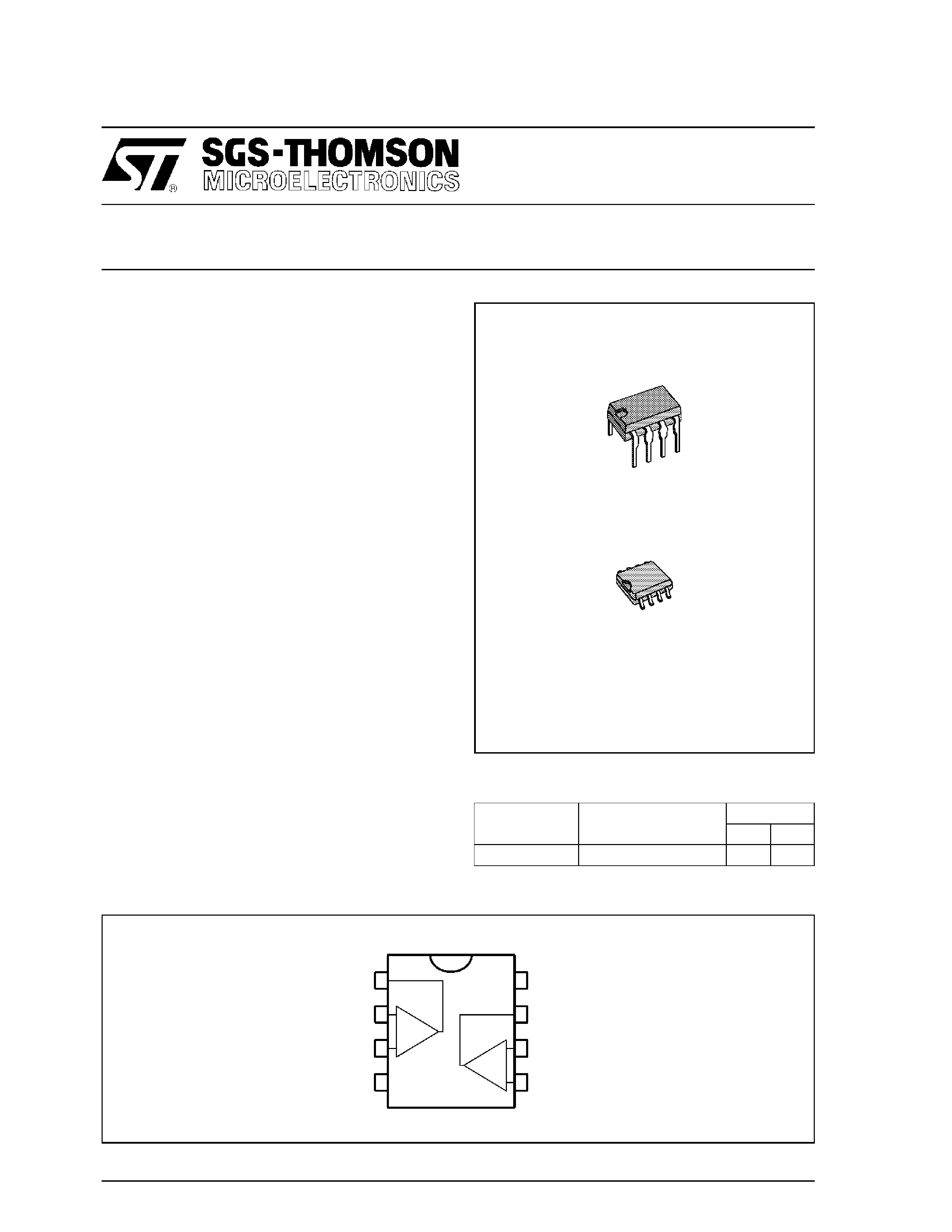
N
DIP8
(Plastic Package)
DESCRIPTION
The MC33078 is a monolithic dual operational
amplifier dedicated to audio applications. The
MC33078 offers low voltage noise (4.5nV/
Hz )
and high frequency performances (15MHz gain
bandwidth product, 7V/
µs slew rate).
In addition the MC33078 has a very low distortion
(0.002%) and excellent phase/gain margins.
The output stage allows a large output voltage
swing and symmetrical source and sink currents.
1
2
3
45
6
7
8
-
+
-
+
Output 1
Inverting input 1
Non-inverting input 1
V
CC
VCC
Output 2
Inverting input 2
Non-inverting input 2
-
+
33078-01.EPS
PIN CONNECTIONS (top view)
D
SO8
(Plastic Micropackage)
ORDER CODES
Part Number
Temperature Range
Package
ND
MC33078
-40, +105
oC
··
33078-01.TBL
1/5
ABSOLUTE MAXIMUM RATINGS
Symbol
Parameter
Value
Unit
VCC
Supply Voltage
±18 or +36
V
Vid
Differential Input Voltage - (note 1)
±30
V
Vi
Input Voltage - (note 1)
±15
V
Output Short-Circuit Duration - (note 2)
Infinite
Toper
Operating Free-air Temperature Range
-40 to +105
oC
Tj
Maximum Junction Temperature
+150
oC
Tstg
Storage Temperature
-65 to +150
oC
Ptot
Maximum Power Dissipation - (note 2)
500
mW
33078-02.TBL
Notes :
1. Either or both input voltages must not exceed the magnitude of VCC+ or VCC-
2. Power dissipation must be considered to ensure maximum junction temperature (Tj) is not exceeded
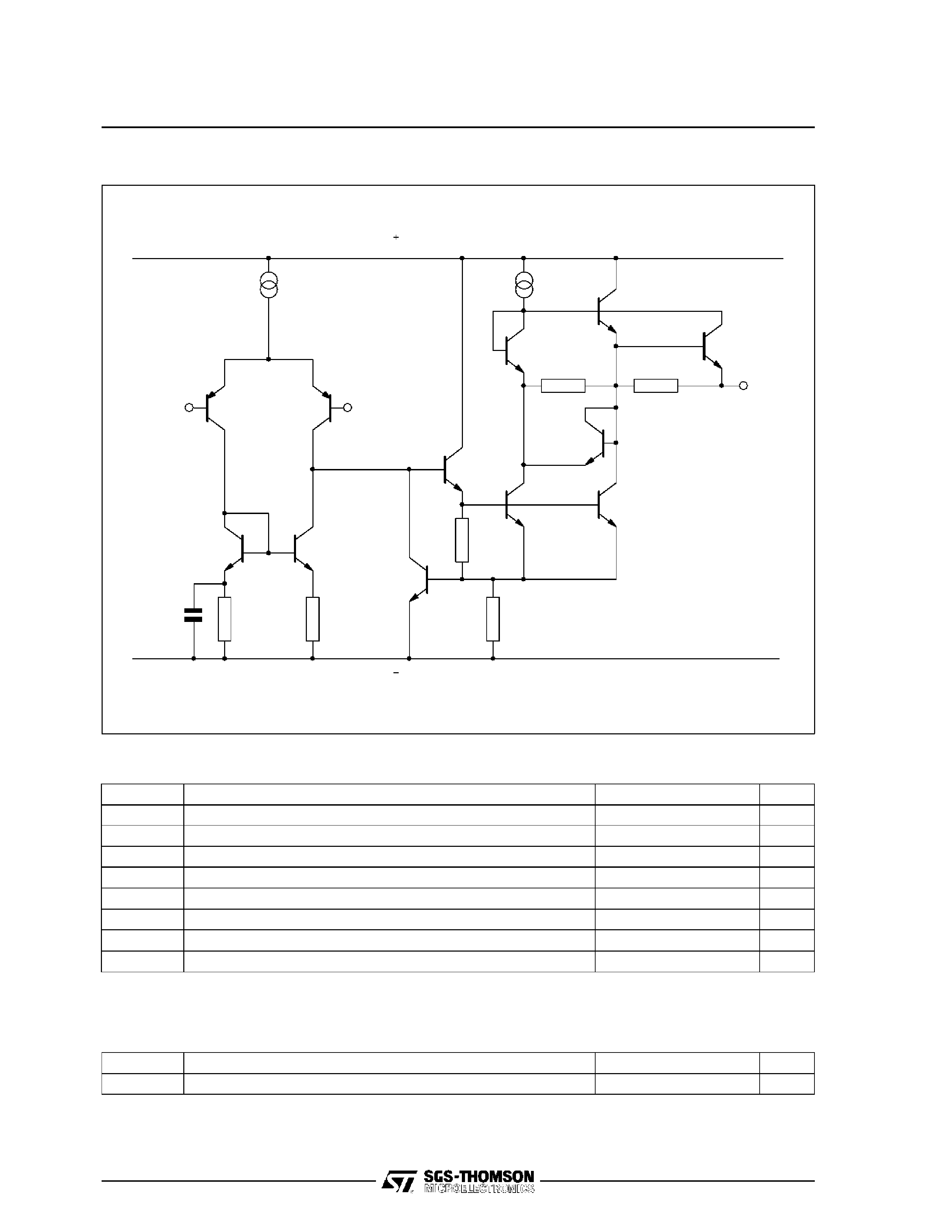
Inverting
Input
Non-inverting
Input
V
CC
Output
V
CC
33078-02.EPS
SCHEMATIC DIAGRAM (1/2 MC33078)
OPERATING CONDITIONS
Symbol
Parameter
Value
Unit
VCC
Supply Voltage
±2.5 to ±15
V
33078-03.TBL
MC33078
2/5
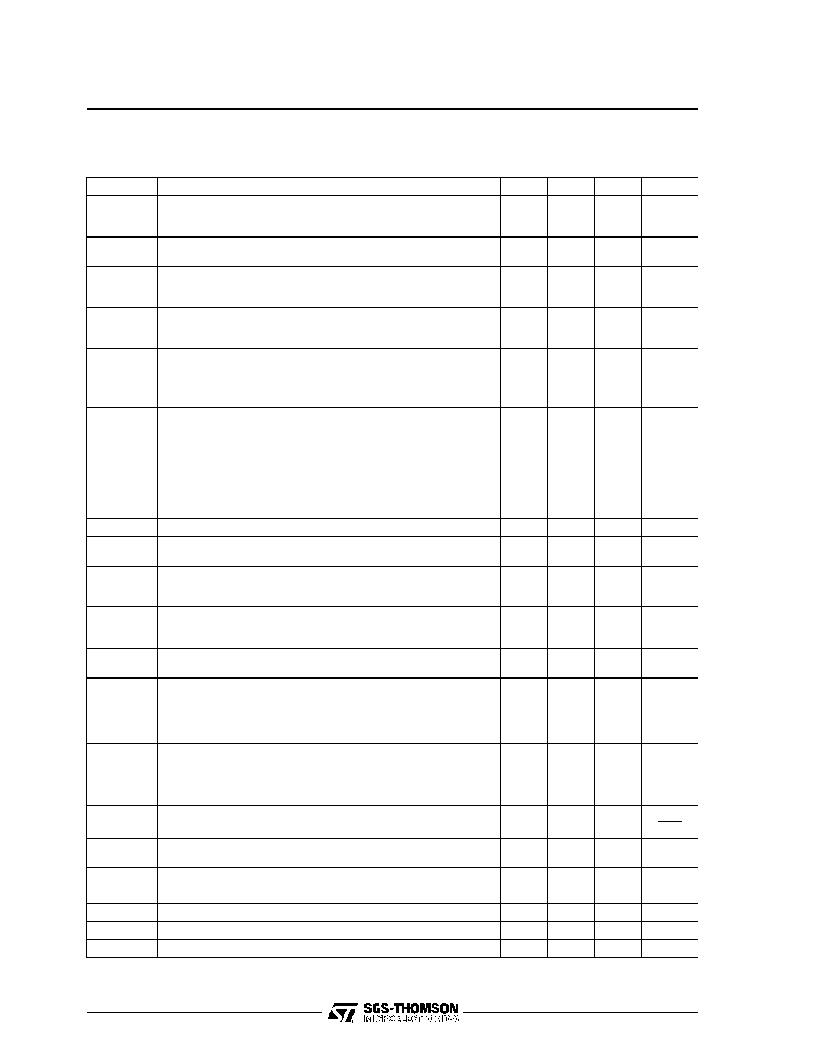
ELECTRICAL CHARACTERISTICS
VCC
+ = +15V, VCC- = -15V, Tamb =25oC (unless otherwise specified)
Symbol
Parameter
Min.
Typ.
Max.
Unit
Vio
Input Offset Voltage (Vo = 0V, Vic = 0V)
Tamb = +25
oC
Tmin.
Tamb Tmax.
0.15
2
3
mV
DVio
Input Offset Voltage Drift
Vic = 0V, Vo = 0V, Tmin.
Tamb Tmax.
2
µV/oC
Iio
Input Offset Current (Vic = 0V, VO = 0V)
Tamb = +25
oC
Tmin.
Tamb Tmax.
10
150
175
nA
Iib
Input Bias Current (Vic = 0V, VO = 0V)
Tamb = +25
oC
Tmin.
Tamb Tmax.
250
750
800
nA
Vicm
Common Mode Input Voltage Range (
VIO = 5mV, VO = 0V)
±13
±14
V
Avd
Large Signal Voltage Gain (RL =2k
,VO = ±10V)
Tamb = +25
oC
Tmin.
Tamb Tmax.
90
85
100
dB
±Vopp
Output Voltage Swing (Vid =
±1V)
RL = 600
RL = 600
RL = 2.0k
RL = 2.0k
RL = 10k
RL = 10k
13.2
13.5
12.2
-12.7
14
-14.2
14.3
-14.6
-13.2
-14
V
CMR
Common Mode Rejection Ratio (Vic =
±13V)
80
100
dB
SVR
Supply Voltage Rejection Ratio
VCC
+ /V
CC
- = +15V / -15V to +5V / -5V
80
105
dB
Io
Output Short Circuit Current (Vid =
±1V, Output to Ground)
Source
Sink
15
20
29
37
mA
ICC
Supply current (VO = 0V, All Amplifiers)
Tamb = +25
oC
Tmin.
Tamb Tmax.
45
5.5
mA
SR
Slew Rate
Vi = -10V to +10V, RL =2k
,CL = 100pF, AV =+1
5
7
V/
µs
GBP
Gain Bandwidth Product (f = 100kHz, RL =2k
,CL = 100pF)
10
15
MHz
B
Unity Gain Bandwidth (Open loop)
9
MHz
Am
Gain Margin (RL =2k
)CL = 0pF
CL = 100pF
-11
-6
dB
m
Phase Margin (RL =2k
)CL = 0pF
CL = 100pF
55
30
Degrees
en
Equivalent Input Noise Voltage (RS = 100
, f = 1kHz)
4.5
nV
Hz
in
Equivalent Input Noise current (f = 1kHz)
0.5
pA
Hz
THD
Total Harmonic Distortion
RL =2k
, f = 20Hz to 20kHz, VO =3Vrms,AV = +1
0.002
%
VO1/VO2
Channel Separation (f = 20Hz to 20kHz)
120
dB
FPB
Full Power Bandwidth (VO = 27Vpp,RL =2k
, THD 1%)
120
kHz
Zo
Output Impedance (VO = 0V, f = 9MHz)
37
Ri
Input Resistance (Vic = 0V)
175
k
Ci
Input Capacitance (Vic = 0V)
12
pF
33078-04.TBL
MC33078
3/5
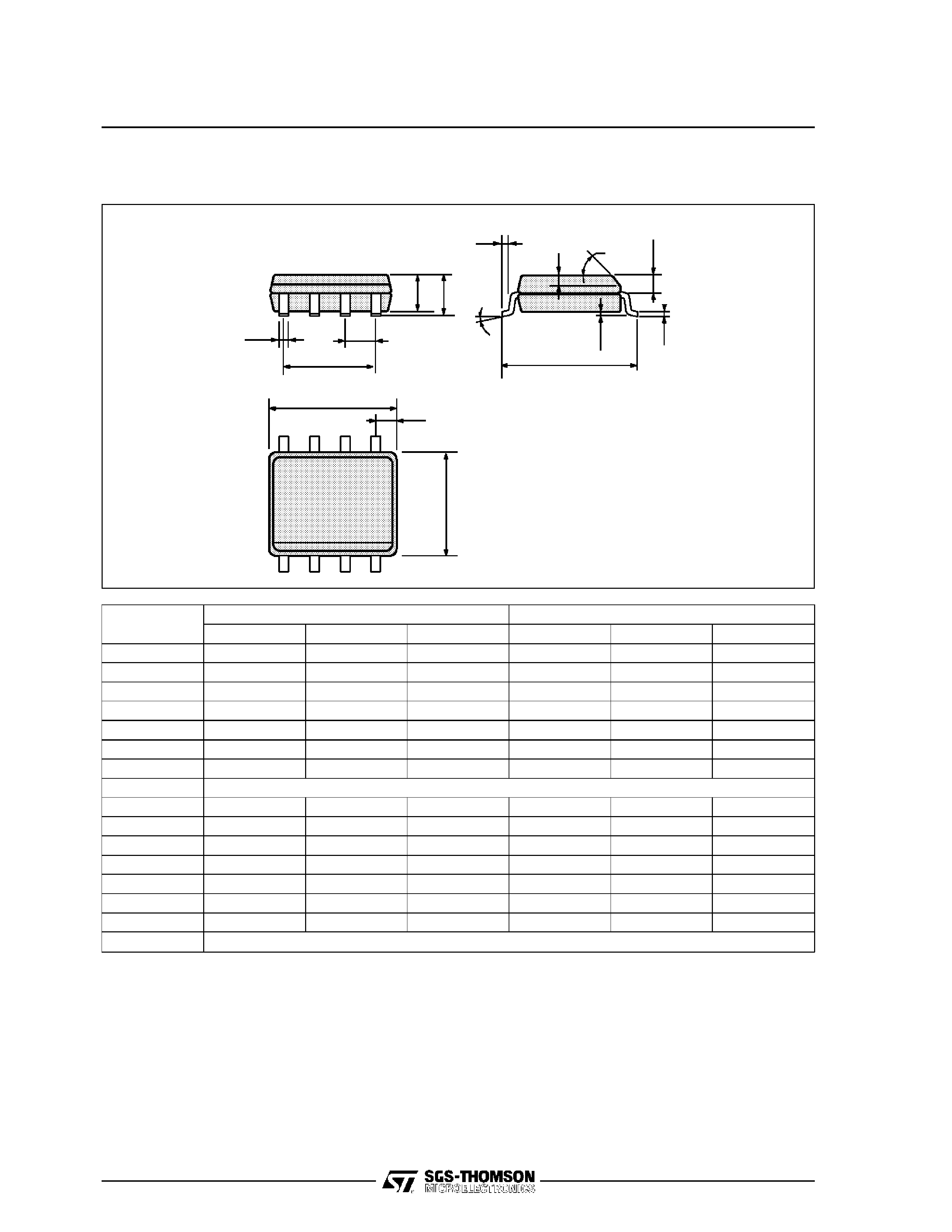
8
14
I
a1
L
B
e
D
b
Z
e3
F
B1
E
5
Z
A
e4
b1
PM-DIP8.EPS
PACKAGE MECHANICAL DATA
8 PINS - PLASTIC DIP
Dimensions
Millimeters
Inches
Min.
Typ.
Max.
Min.
Typ.
Max.
A
3.32
0.131
a1
0.51
0.020
B
1.15
1.65
0.045
0.065
b
0.356
0.55
0.014
0.022
b1
0.204
0.304
0.008
0.012
D
10.92
0.430
E
7.95
9.75
0.313
0.384
e
2.54
0.100
e3
7.62
0.300
e4
7.62
0.300
F
6.6
0260
i
5.08
0.200
L
3.18
3.81
0.125
0.150
Z
1.52
0.060
DIP8.TBL
MC33078
4/5
Information furnished is believed to be accurate and reliable. However, SGS-THOMSON Microelectronics assumes no responsibility
for the consequences of use of such information nor for any infringement of patents or other rights of third parties which may result
from its use. No licence is granted by implication or otherwise under any patent or patent rights of SGS-THOMSON Microelectronics.
Specifications mentioned in this publication are subject to change without notice. This pub lication supersedes and replaces all
information previously supplied. SGS-THOMSON Microelectronics products are not authorized for use as critical components in life
support devices or systems without express written approval of SGS-THOMSON Microelectronics.
© 1994 SGS-THOMSON Microelectronics - All Rights Reserved
SGS-THOMSON Microelectronics GROUP OF COMPANIES
Australia - Brazil - France - Germany - Hong Kong - Italy - Japan - Korea - Malaysia - Malta - Morocco - The Netherlands
Singapore - Spain - Sweden - Switzerland - Taiwan - Thailand - United Kingdom - U.S.A.
ORDER
CODE
:
F
C
L
E
a1
b1
a2
A
e
D
M
e3
b
8
5
14
c1
s
a3
PM-SO8.EPS
PACKAGE MECHANICAL DATA
8 PINS - PLASTIC MICROPACKAGE (SO)
Dimensions
Millimeters
Inches
Min.
Typ.
Max.
Min.
Typ.
Max.
A
1.75
0.069
a1
0.1
0.25
0.004
0.010
a2
1.65
0.065
a3
0.65
0.85
0.026
0.033
b
0.35
0.48
0.014
0.019
b1
0.19
0.25
0.007
0.010
C
0.25
0.5
0.010
0.020
c1
45
o (typ.)
D
4.8
5.0
0.189
0.197
E
5.8
6.2
0.228
0.244
e
1.27
0.050
e3
3.81
0.150
F
3.8
4.0
0.150
0.157
L
0.4
1.27
0.016
0.050
M
0.6
0.024
S8
o (max.)
SO8.TBL
MC33078
5/5