XP-SN70
US Model
Canadian Model
AEP Model
E Model
SERVICE MANUAL
PORTABLE CD PLAYER
Sony Corporation
Personal Audio Company
Published by Sony Engineering Corporation
9-961-142-02
2003J16-1
© 2003.10
SPECIFICATIONS
Ver 1.1 2003. 10
Model Name Using Similar Mechanism
NEW
CD Mechanism Type
CDM-3325EK
Optical Pick-up Name
DAX-25E
System
Compact disc digital audio system
Laser diode properties
Material: GaAlAs
Wavelength:
= 780 nm
Emission duration: Continuous
Laser output: Less than 44.6
µW
(This output is the value measured at a distance
of 200 mm from the objective lens surface on
the optical pick-up block with 7 mm aperture.)
D-A conversion
1-bit quartz time-axis control
Frequency response
20 - 20 000 Hz
+1
2 dB (measured by JEITA CP-
307)
Output (at 4.5 V input level)
Headphones (stereo minijack):
Approx. 5 mW + Approx. 5 mW at 16
Power requirements
For the area code of the model you
purchased, check the upper left side of the
bar code on the package.
·Two LR6 (size AA) batteries: 1.5 V DC
× 2
·AC power adaptor (DC IN 4.5 V jack):
Battery life*1 (approx. hours)
(When you use the CD player on a flat and stable
surface)
Playing time varies depending on how the CD
player is used.
When using two Sony alkaline batteries
LR6 (SG) (produced in Japan)
E·A·S·S GP
12
Audio CD
50
45
ATRAC3plus files*2
77
MP3 files*3
72
*1 Measured value by the standard of JEITA
(Japan Electronics and Information Technology
Industries Association)
*2 When recorded at 48 kbps or 64 kbps
*3 When recorded at 128 kbps
Operating temperature
5
°C - 35°C (41°F - 95°F)
Dimensions (w/h/d) (excluding
projecting parts and controls)
Approx. 133
× 34 × 151 mm
(5 1/4
× 1 3/8 × 6 in.)
Mass (excluding accessories)
Approx. 341 g (12.0 oz.)
Design and specifications are subject to change
without notice.
Headphones (1)
Hand strap (1)
AC power adaptor* (1)
CD-ROM (SonicStage Simple Burner)** (1)
* Not supplied with the U model. For the area
code of the model you purchased, check the
upper left side of the bar code on the package.
** Do not play a CD-ROM on an audio CD player.
US, Canadian models: 120V, 60Hz
AEP, MX models
: 100-240V, 50/60Hz
·Abbreviation
MX
: Mexican model
2
XP-SN70
Flexible Circuit Board Repairing
· Keep the temperature of the soldering iron around 270 °C during repairing.
· Do not touch the soldering iron on the same conductor of the
circuit board (within 3 times).
· Be careful not to apply force on the conductor when soldering
or unsoldering.
Notes on chip component replacement
·Never reuse a disconnected chip component.
· Notice that the minus side of a tantalum capacitor may be damaged by heat.
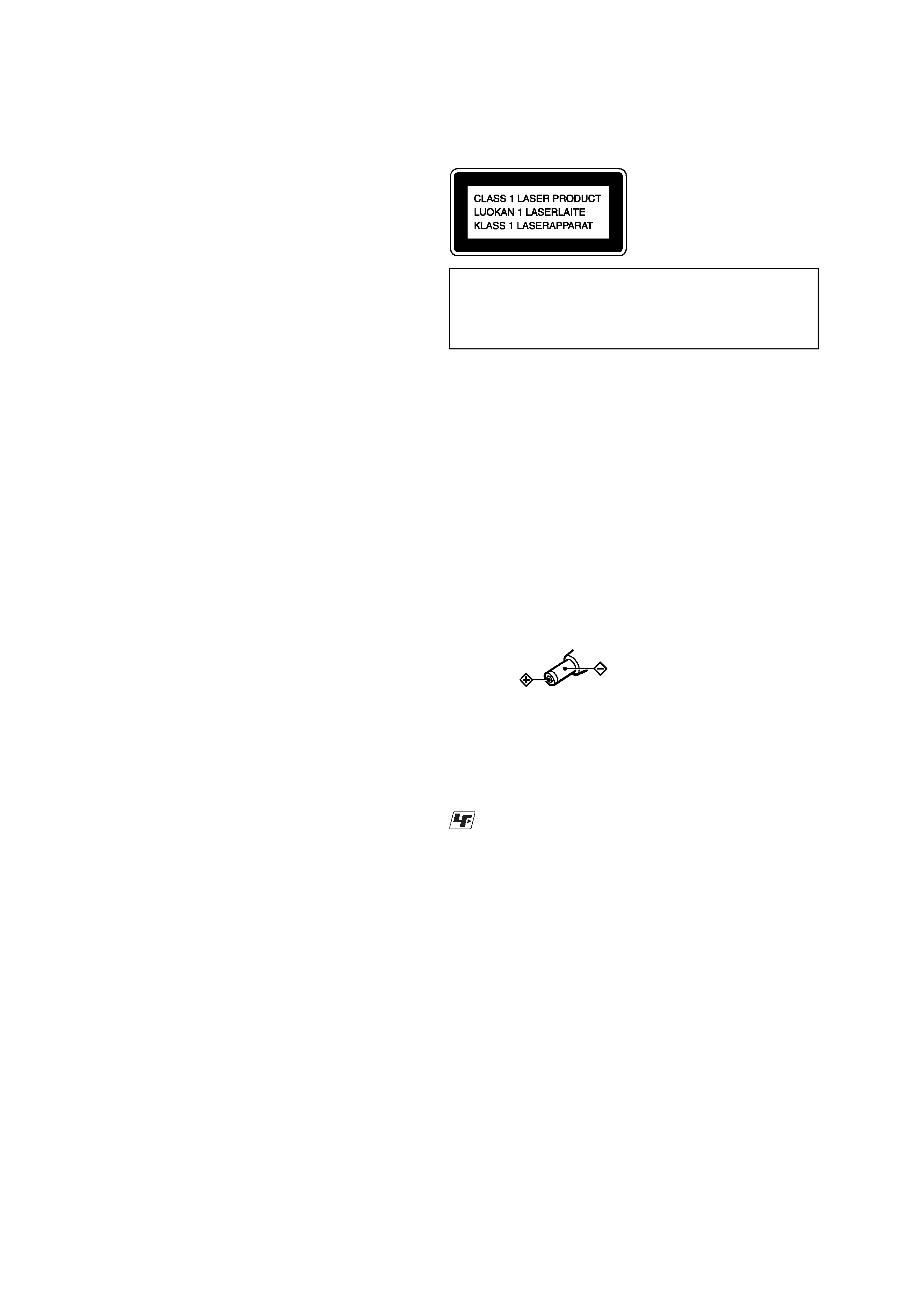
This appliance is classified as a CLASS 1 LASER product.
The CLASS 1 LASER PRODUCT MARKING is located on
the rear exterior.
CAUTION
Use of controls or adjustments or performance of procedures
other than those specified herein may result in hazardous
radiation exposure.
On AC poweradaptor
· Use only the commercially-available AC power
adaptor whose rated output is 4.5 V DC, 500 mA.
Do not use any other AC power adaptor. It may
cause a malfunction.
Polarity of the plug
TABLE OF CONTENTS
1. SERVICING NOTE ·························································· 3
2. GENERAL ·········································································· 5
3. DISASSEMBLY
3-1. CABINET (UPPER) SUB ASSY,
PANEL (UPPER) LID ASSY ········································ 6
3-2. CONTROL BOARD ····················································· 7
3-3. CD MECHANISM (CDM-3325EK) ····························· 7
3-4. MAIN BOARD ····························································· 8
3-5. MOTOR ASSY (SLED)(M902),
OPTICAL PICK-UP (DAX-25E),
TURN TABLE MOTOR ASSY (SPINDLE)(M901) ···· 8
4. ELECTRICAL CHECKING ··········································· 9
5. DIAGRAMS ······································································ 10
5-1. BLOCK DIAGRAM ··················································· 11
5-2. PRINTED WIRING BOARDS
MAIN BOARD (SIDE A) ····································· 12
5-3. PRINTED WIRING BOARDS
MAIN BOARD (SIDE B) ····································· 13
5-4. SCHEMATIC DIAGRAMS
MAIN BOARD (1/4) ············································· 14
5-5. SCHEMATIC DIAGRAMS
MAIN BOARD (2/4) ············································· 15
5-6. SCHEMATIC DIAGRAMS
MAIN BOARD (3/4) ············································· 16
5-7. SCHEMATIC DIAGRAMS
MAIN BOARD (4/4) ············································· 17
5-8. PRINTED WIRING BOARDS
CONTROL BOARD ············································· 18
5-9. SCHEMATIC DIAGRAMS
CONTROL BOARD ············································· 19
5-10. IC BLOCK DIAGRAMS ············································ 20
5-11. IC PIN FUNCTION DESCRIPTIONS ······················· 21
6. EXPLODED VIEWS
6-1. CABINET (UPPER) SECTION ·································· 23
6-2. CABINET (LOWER) SECTION ································ 24
6-3. CD MECHANISM SECTION (CDM-3325EK) ········· 25
7. ELECTRICAL PARTS LIST ······································· 26
SAFETY-RELATED COMPONENT WARNING!!
COMPONENTS IDENTIFIED BY MARK 0 OR DOTTED LINE WITH
MARK 0 ON THE SCHEMATIC DIAGRAMS AND IN THE PARTS
LIST ARE CRITICAL TO SAFE OPERATION. REPLACE THESE
COMPONENTS WITH SONY PARTS WHOSE PART NUMBERS
APPEAR AS SHOWN IN THIS MANUAL OR IN SUPPLEMENTS
PUBLISHED BY SONY.
ATTENTION AU COMPOSANT AYANT RAPPORT
À LA SÉCURITÉ!
LES COMPOSANTS IDENTIFÉS PAR UNE MARQUE 0 SUR LES
DIAGRAMMES SCHÉMATIQUES ET LA LISTE DES PIÈCES SONT
CRITIQUES POUR LA SÉCURITÉ DE FONCTIONNEMENT. NE
REMPLACER CES COMPOSANTS QUE PAR DES PIÈSES SONY
DONT LES NUMÉROS SONT DONNÉS DANS CE MANUEL OU
DANS LES SUPPÉMENTS PUBLIÉS PAR SONY.
Unleaded solder
Boards requiring use of unleaded solder are printed with the lead-
free mark (LF) indicating the solder contains no lead.
(Caution: Some printed circuit boards may not come printed with
the lead free mark due to their particular size.)
: LEAD FREE MARK
Unleaded solder has the following characteristics.
· Unleaded solder melts at a temperature about 40
°C higher than
ordinary solder.
Ordinary soldering irons can be used but the iron tip has to be
applied to the solder joint for a slightly longer time.
Soldering irons using a temperature regulator should be set to
about 350
°C.
Caution: The printed pattern (copper foil) may peel away if the
heated tip is applied for too long, so be careful!
· Strong viscosity
Unleaded solder is more viscous (sticky, less prone to flow) than
ordinary solder so use caution not to let solder bridges occur such
as on IC pins, etc.
· Usable with ordinary solder
It is best to use only unleaded solder but unleaded solder may
also be added to ordinary solder.
3
XP-SN70
SECTION 1
SERVICING NOTE
The laser diode in the optical pick-up block may suffer electrostatic
breakdown because of the potential difference generated by the
charged electrostatic load, etc. on clothing and the human body.
During repair, pay attention to electrostatic breakdown and also use
the procedure in the printed matter which is included in the repair
parts.
The flexible board is easily damaged and should be handled with
care.
NOTES ON LASER DIODE EMISSION CHECK
The laser beam on this model is concentrated so as to be focused on
the disc reflective surface by the objective lens in the optical pick-
up block. Therefore, when checking the laser diode emission,
observe from more than 30 cm away from the objective lens.
BEFORE REPLACING THE OPTICAL PICK-UP BLOCK
Please be sure to check thoroughly the parameters as par the "Optical
Pick-Up Block Checking Procedures" (Part No.: 9-960-027-11)
issued separately before replacing the optical pick-up block.
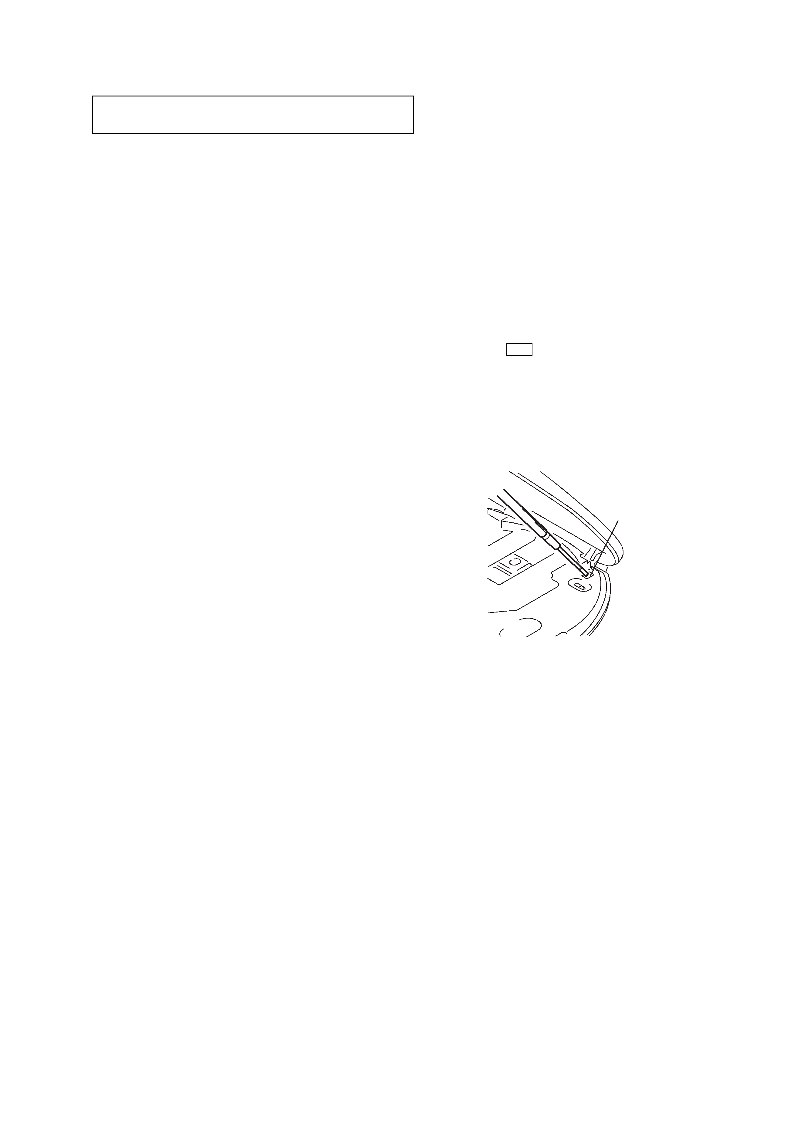
LASER DIODE AND FOCUS SEARCH OPERATION
CHECK
During normal operation of the equipment, emission of the laser
diode is prohibited unless the upper lid is closed while turning ON
the S820. (push switch type)
The following checking method for the laser diode is operable.
· Method:
Emission of the laser diode is visually checked.
1. Open the upper lid.
2. With a disc not set, turn on the S820 with a screwdriver having a
thin tip as shown in Fig.1.
3. Press the u button.
4. Observing the objective lens, check that the laser diode emits
light.
When the laser diode does not emit light, automatic power control
circuit or optical pickup is faulty.
In this operation, the objective lens will move up and down 4
times along with inward motion for the focus search.
NOTES ON HANDLING THE OPTICAL PICK-UP
BLOCK OR BASE UNIT
Fig. 1 Method to push the S820
S820
(OPEN/CLOSE switch)
4
XP-SN70
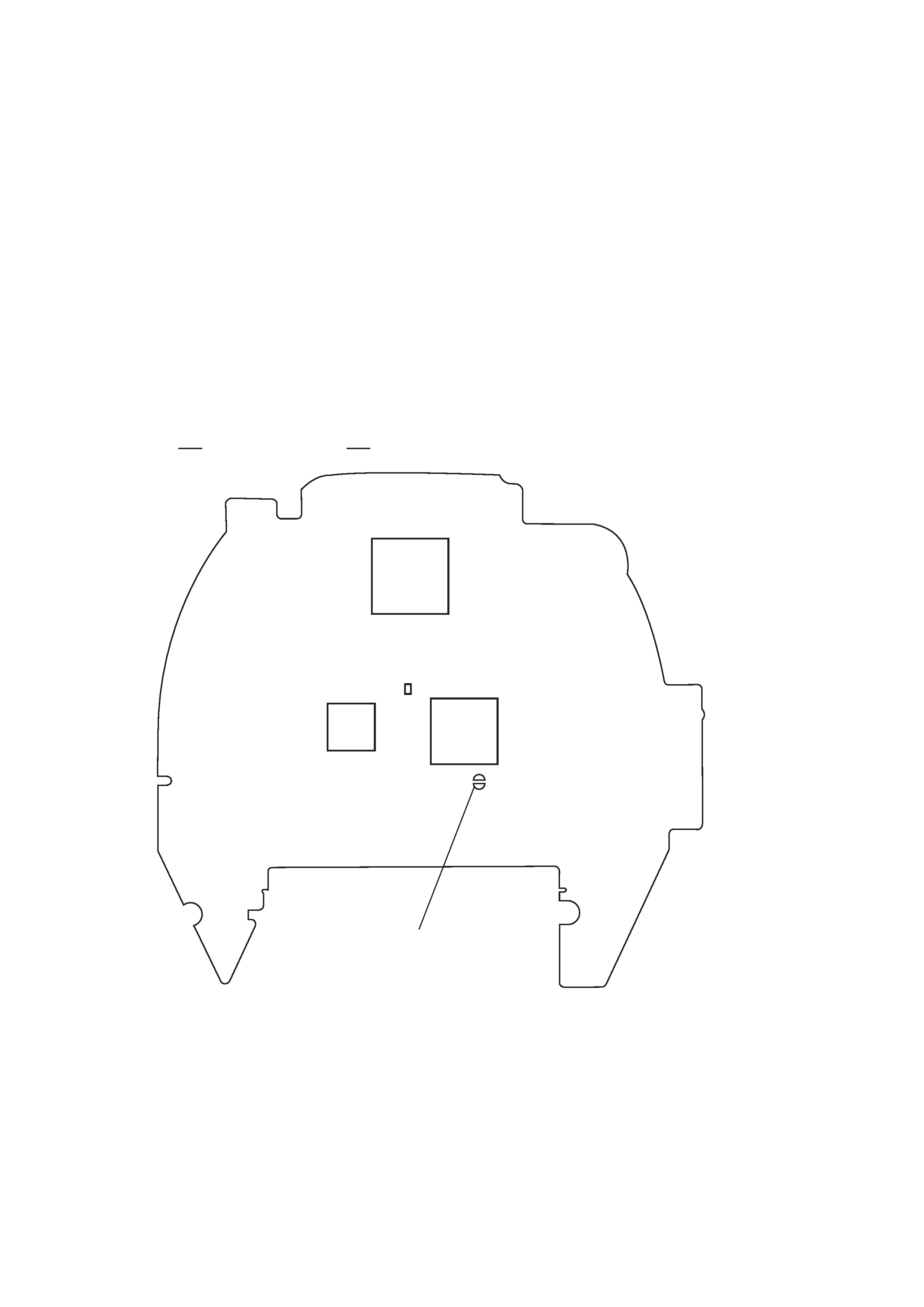
TEST MODE
The software version display and LCD test can be performed when
the test mode is activated.
Procedure:
1. Confirm the set is not powered on. (Remove two batteries and
disconnect the AC power adaptor.)
2. Short the solder land SL806 (TEST) on the MAIN board.
3. Turn on the main power. (Insert two batteries.)
4. Microcomputer version is displayed for about a second.
5. After that all segments of the liquid crystal display are turned on.
6. Turn off the main power. (Remove two batteries.)
7. Open the solder land SL806 (TEST) on the MAIN board.
Note : The solder should be removed clean.
IC601
IC802
IC801
IC701
SL806
(TEST)
MAIN BOARD (SIDE A)
5
XP-SN70
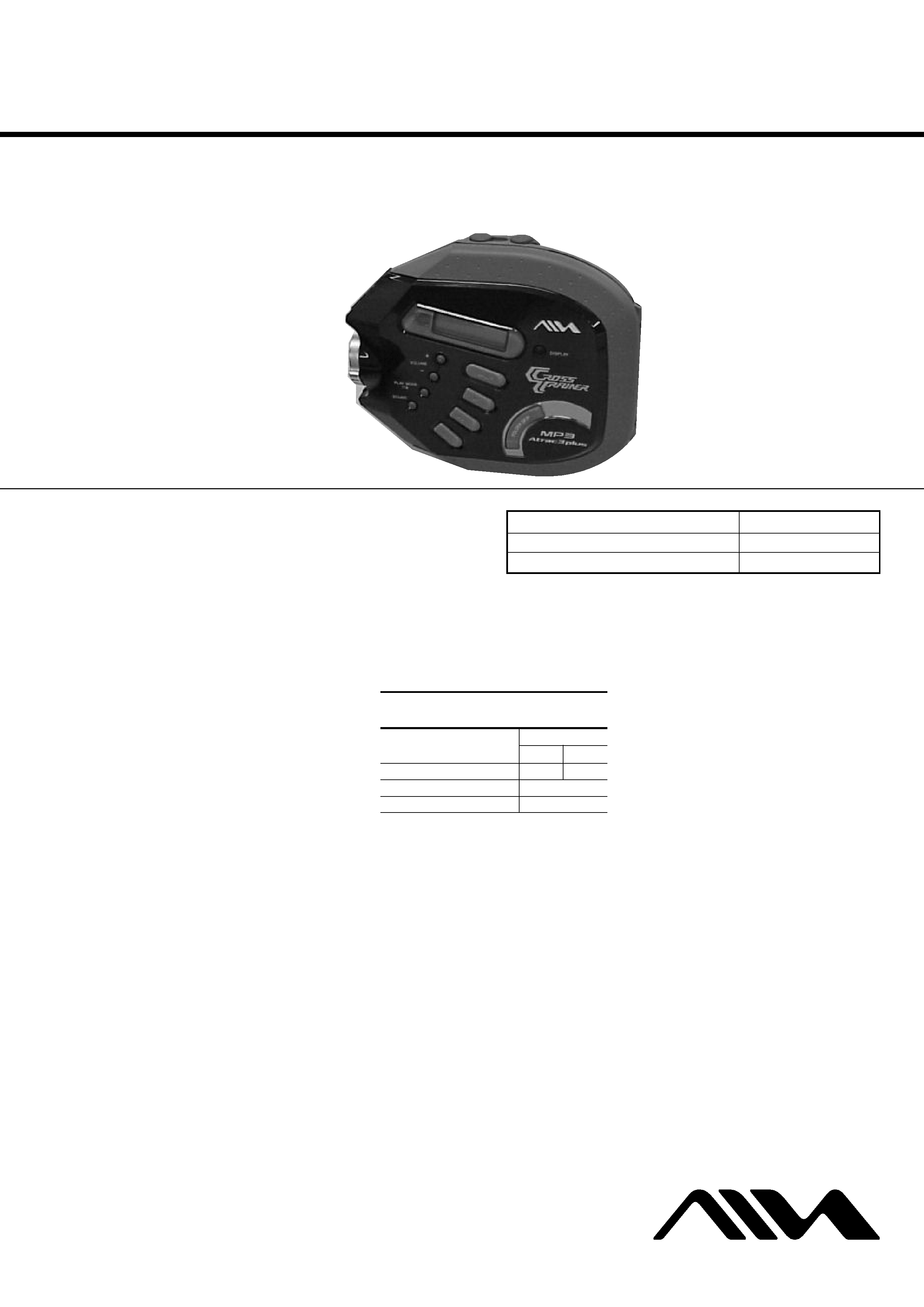
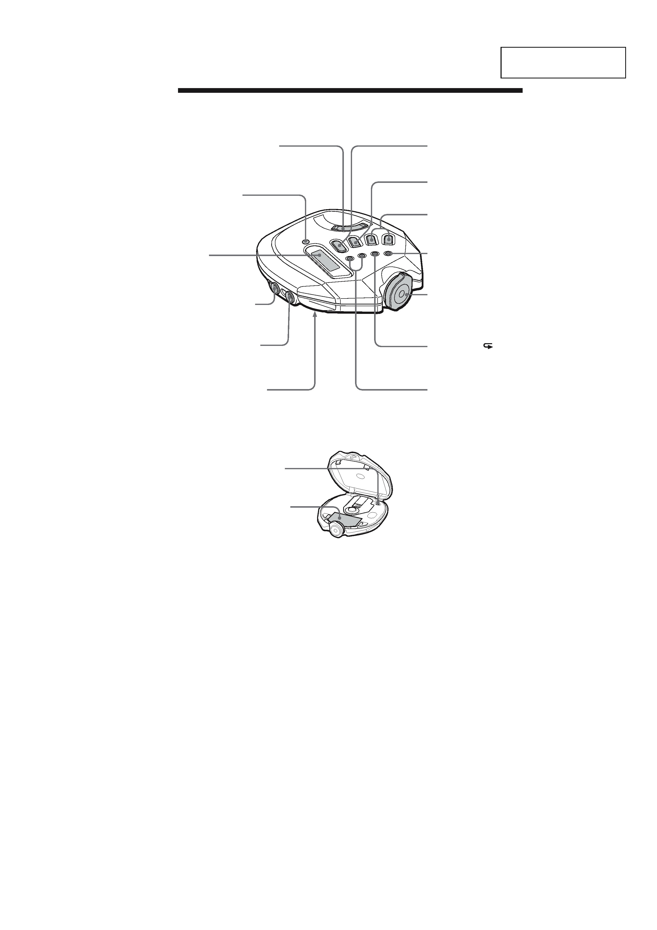
SECTION 2
GENERAL
This section is extracted
from instruction manual.
Locating the controls
CD player (front)
CD player (inside)
Battery compartment
(pages 10, 23)
E·A·S·S GP switch
(page 20)
* The button has a tactile dot.
FOLDER SKIP +/ buttons
(page 12)
DISPLAY button
(pages 20, 21)
Display
(pages 13, 16, 19-23)
i (headphones) jack
(page 10)
DC IN 4.5 V (external
power input) jack (page 23)
HOLD switch (page 22)
u* (play/pause) button
(pages 11, 12, 16, 18, 19)
x (stop) button
(pages 12, 22)
./> (skip/search)
buttons (pages 12, 16, 19)
SOUND button
(pages 21, 22)
OPEN/LOCK knob
(pages 10, 11)
PLAY MODE/
(repeat)
button (pages 16-19)
VOLUME +*/ buttons
(page 11)