XP-EV500/EV500C
EV500N/EV501R
US Model
XP-EV501R
Canadian Model
XP-EV500N
AEP Model
XP-EV500/EV501R
UK Model
XP-EV500
E Model
XP-EV500/EV500C/EV500N
Australian Model
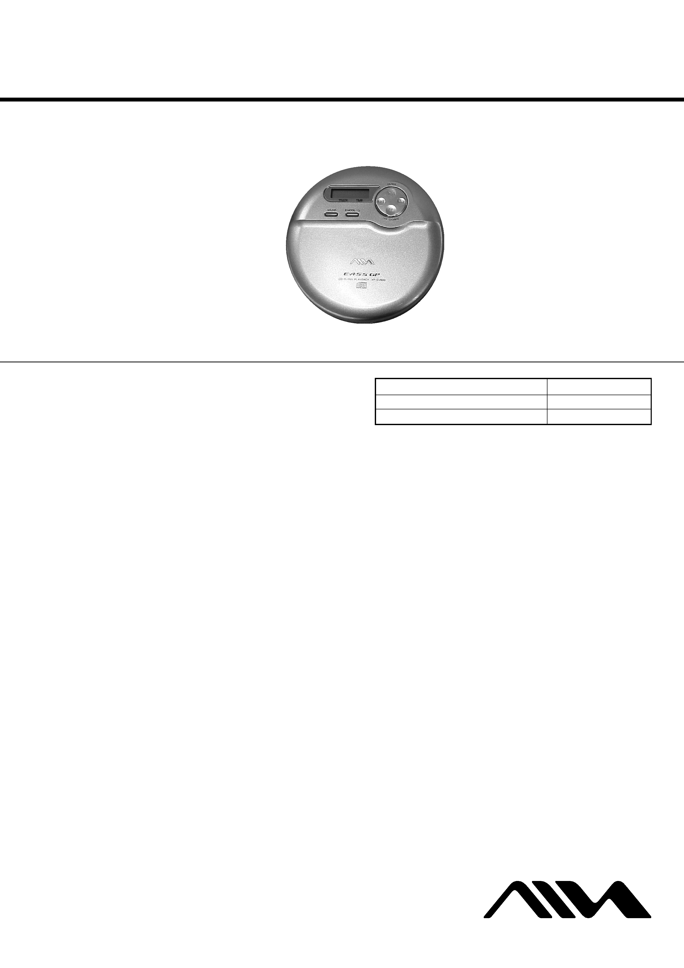
XP-EV500
SERVICE MANUAL
PORTABLE CD PLAYER
Sony Corporation
Personal Audio Company
Published by Sony Engineering Corporation
9-877-200-03
2003H16-1
© 2003.08
SPECIFICATIONS
Ver 1.2 2003. 08
Model Name Using Similar Mechanism
D-E760
CD Mechanism Type
CDM-3325ER
Optical Pick-up Name
DAX-25E
Photo: XP-EV500
System
Compact disc digital audio system
Laser diode properties
Material: GaAlAs
Wavelength:
= 780 nm
Emission duration: Continuous
Laser output: Less than 44.6
µW (This output is the value
measured at a distance of 200 mm from the objective lens
surface on the optical pick-up block with 7 mm aperture.)
Power requirements
· Two LR6 (size AA) batteries (not supplied): 3 V DC
· AC power adaptor (DC IN 4.5 V jack)
· Two Ni-MH rechargeable batteries (size AA): 2.4 V DC
Dimensions (w/h/d) (without projecting
parts and controls)
Approx. 136
× 20.4 × 139 mm (5 3/8 × 13/16 × 5 1/2 in.)
Mass (excluding accessories)
Approx. 175 g (6 oz)
Operating temperature
5
°C - 35°C (41°F - 95°F)
Design and specifications are subject to change without
notice.
Supplied Accessories
XP-EV500:
XP-EV500N:
XP-EV501R:
Earphones (1)
AC power adaptor (1)
Earphones (1)
Headphones with the remote control (1)
XP-EV500C: Ileadphones/Earphones (1)
AC power adaptor (1)
Car connecting pack (1)
Car battery cord (1)
Velcro tape (2)
2
XP-EV500/EV500C/EV500N/EV501R
Flexible Circuit Board Repairing
·Keep the temperature of the soldering iron around 270 °C dur-
ing repairing.
· Do not touch the soldering iron on the same conductor of the
circuit board (within 3 times).
· Be careful not to apply force on the conductor when soldering
or unsoldering.
Notes on chip component replacement
·Never reuse a disconnected chip component.
· Notice that the minus side of a tantalum capacitor may be dam-
aged by heat.
On AC poweradaptor
· Use only the commercially-available AC power adaptor whose
rated output is 4.5 V DC, 500 mA. Do not use any other AC
power adaptor. It may cause a malfunction.
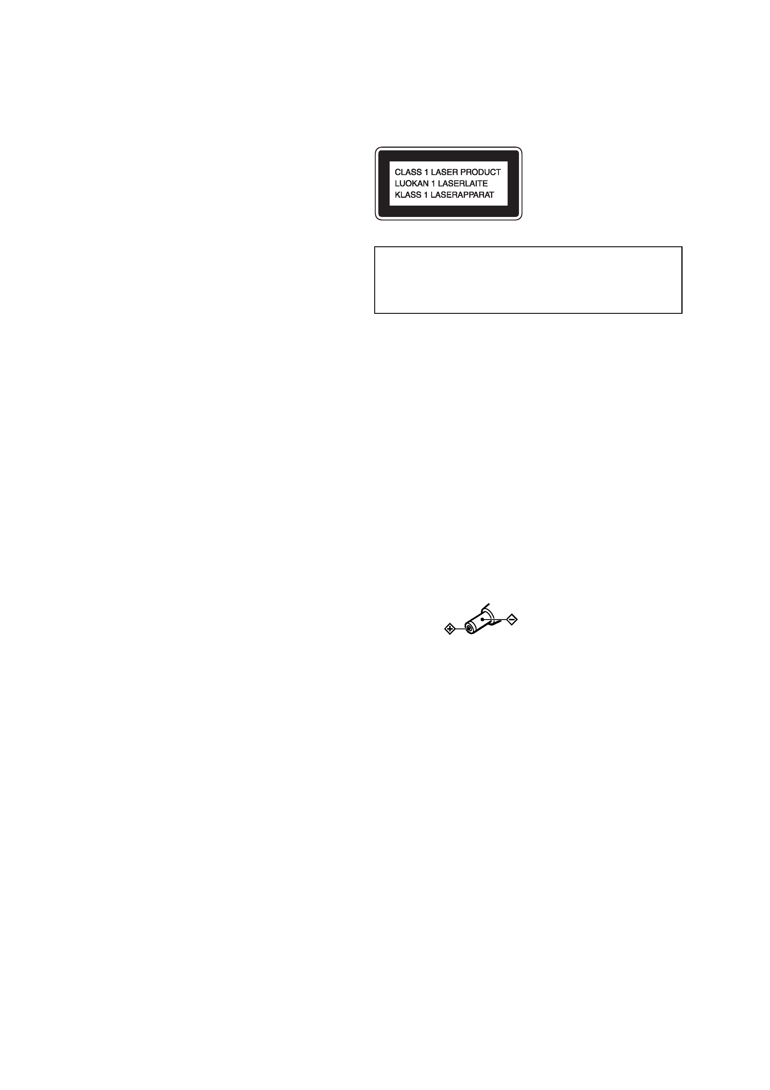
This appliance is classified as a CLASS 1 LASER product.
The CLASS 1 LASER PRODUCT MARKING is located on
the rear exterior.
CAUTION
Use of controls or adjustments or performance of procedures
other than those specified herein may result in hazardous
radiation exposure.
TABLE OF CONTENTS
1. SERVICING NOTE ·························································· 3
2. GENERAL ·········································································· 4
3. DISASSEMBLY ································································ 5
3-1. Lower Cabinet Section ·················································· 6
3-2. CD Mechanism Section (CDM-3325ER) ······················ 7
3-3. Cabinet (front) Sub Assy ··············································· 8
3-4. Upper Lid Sub Assy ······················································ 9
3-5. MAIN Board ······························································· 10
3-6. Motor Assy (sled) (M902),
Optical Pick-up (DAX-25E),
Turn Table Motor Assy (spindle) (M901) ··················· 10
4. ELECTRICAL CHECKING ········································· 11
5. DIAGRAMS ······································································ 12
5-1. Block Diagram ···························································· 13
5-2. Printed Wiring Board MAIN Board (SIDE A) ······ 14
5-3. Printed Wiring Board MAIN Board (SIDE B) ······ 15
5-4. Schematic Diagram MAIN Board (1/4) ················ 16
5-5. Schematic Diagram MAIN Board (2/4) ················ 17
5-6. Schematic Diagram MAIN Board (3/4) ················ 18
5-7. Schematic Diagram MAIN Board (4/4) ················ 19
5-8. IC Block Diagram ······················································· 20
5-9. IC Pin Function Description ········································ 21
6. EXPLODED VIEWS
6-1. Cabinet Upper Section ················································· 23
6-2. Cabinet Lower Section ················································ 24
6-3. CD Mechanism Deck Section (CDM-3325ER) ·········· 25
7. ELECTRICAL PARTS LIST ······································· 26
SAFETY-RELATED COMPONENT WARNING!!
COMPONENTS IDENTIFIED BY MARK 0 OR DOTTED LINE WITH
MARK 0 ON THE SCHEMATIC DIAGRAMS AND IN THE PARTS
LIST ARE CRITICAL TO SAFE OPERATION. REPLACE THESE
COMPONENTS WITH SONY PARTS WHOSE PART NUMBERS
APPEAR AS SHOWN IN THIS MANUAL OR IN SUPPLEMENTS
PUBLISHED BY SONY.
Polarity of the plug
3
XP-EV500/EV500N/EV501R
SECTION 1
SERVICING NOTE
The laser diode in the optical pick-up block may suffer electrostatic
breakdown because of the potential difference generated by the
charged electrostatic load, etc. on clothing and the human body.
During repair, pay attention to electrostatic breakdown and also use
the procedure in the printed matter which is included in the repair
parts.
The flexible board is easily damaged and should be handled with
care.
NOTES ON LASER DIODE EMISSION CHECK
The laser beam on this model is concentrated so as to be focused on
the disc reflective surface by the objective lens in the optical pick-
up block. Therefore, when checking the laser diode emission,
observe from more than 30 cm away from the objective lens.
BEFORE REPLACING THE OPTICAL PICK-UP BLOCK
Please be sure to check thoroughly the parameters as par the "Optical
Pick-Up Block Checking Procedures" (Part No.: 9-960-027-11)
issued separately before replacing the optical pick-up block.
Note and specifications required to check are given below.
· FOK output: IC301 9 pin
When checking FOK, remove the lead wire to disc motor.
· RF signal P-to-P value: 0.45 to 0.70 Vp-p
LASER DIODE AND FOCUS SEARCH OPERATION
CHECK
During normal operation of the equipment, emission of the laser
diode is prohibited unless the upper lid is closed while turning ON
the S303. (push switch type)
The following checking method for the laser diode is operable.
· Method:
Emission of the laser diode is visually checked.
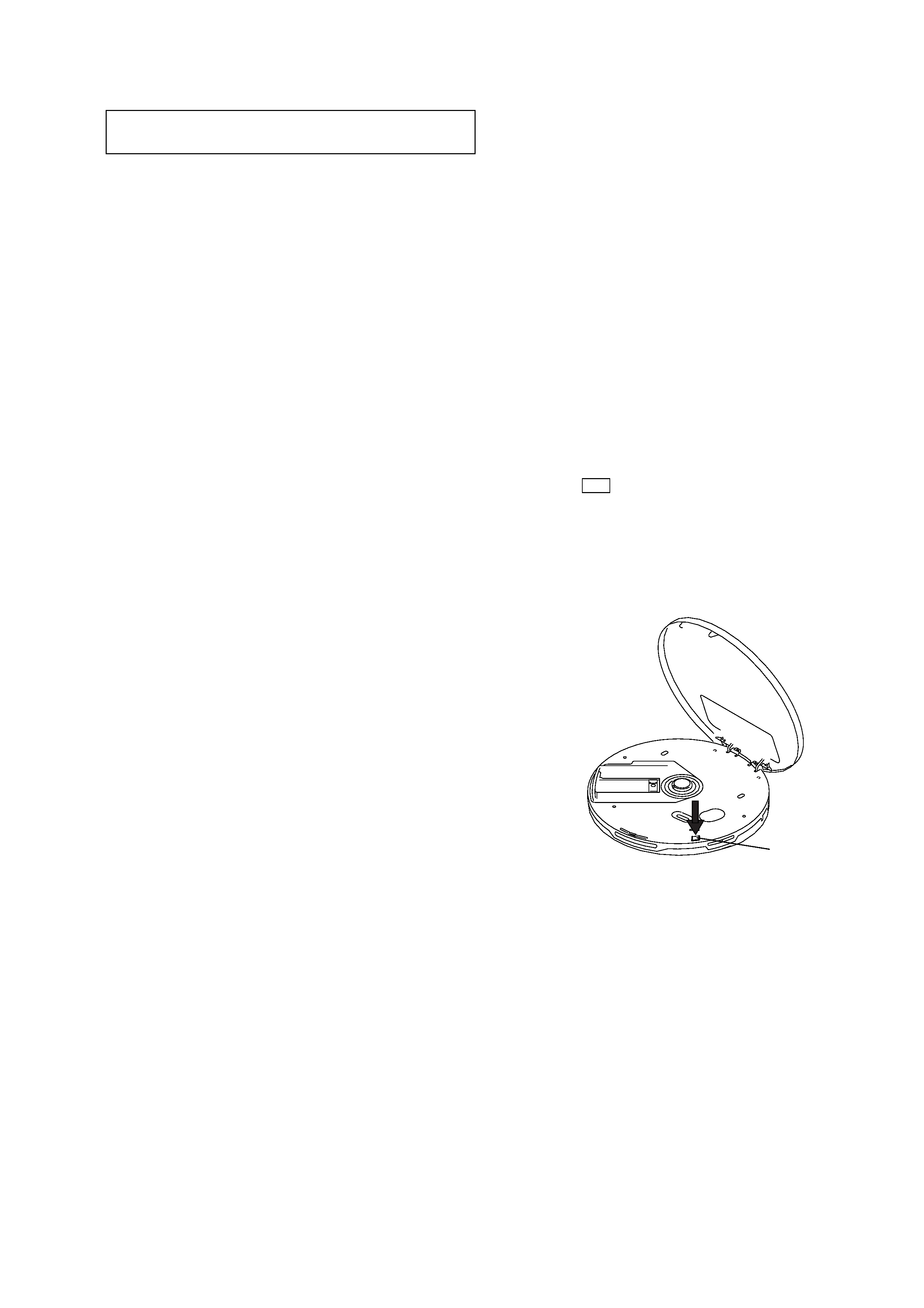
1. Open the upper lid.
2. With a disc not set, turn on the S303 with a screwdriver having a
thin tip as shown in Fig.1.
3. Press the u button.
4. Observing the objective lens, check that the laser diode emits
light.
When the laser diode does not emit light, automatic power control
circuit or optical pickup is faulty.
In this operation, the objective lens will move up and down 4
times along with inward motion for the focus search.
NOTES ON HANDLING THE OPTICAL PICK-UP
BLOCK OR BASE UNIT
Fig. 1 Method to push the S303
S303
4
XP-EV500/EV500N/EV501R
SECTION 2
GENERAL
This section is extracted
from instruction manual.
CD player (front)
CD player (rear/inside)
Remote control (XP-EV501R only)
Display
*The button has a tactile dot.
A
B
2SOUND
\
(headphones)
jack
6HOLD
DC IN 4.5 V
(external power
input) jack
7VOL +*/
5s(stop)/OFF/
CHARGE
Display
1P-MODE/
Strap holes
4ca *(play/
pause)/ENTER
3r/t
(skip/search)
OPEN
8E·A·S·S
Insert the ( end first (for both
batteries).
Open the battery
compartment lid.
Play mode
Track number
Playing time
Remaining battery power
Sound mode
CHG
4ca
7VOL
Headphones
jack
3tF SKIP
3rB SKIP
2SOUND
6HOLD
5s
5
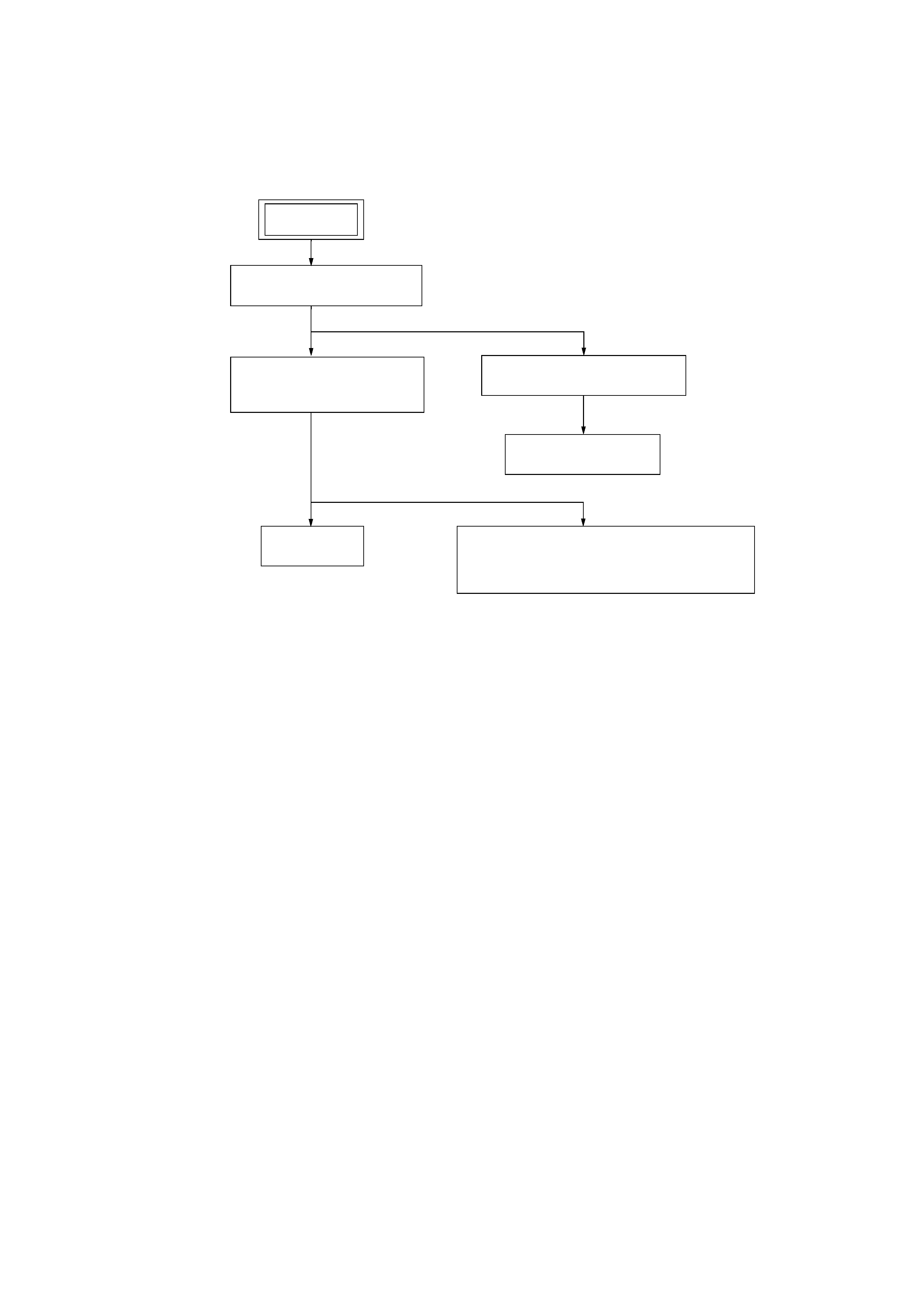
XP-EV500/EV500N/EV501R
SECTION 3
DISASSEMBLY
Note :
Disassemble the unit in the order as shown below.
LOWER CABINET SECTION
CABINET (FRONT) SUB ASSY
UPPER LID SUB ASSY
CD MECHANISM SECTION
(CDM-3325ER)
MAIN BOARD
SET
MOTOR ASSY (SLED) (M902),
OPTICAL PICK-UP (DAX-25E),
TURN TABLE MOTOR ASSY (SPINDLE) (M901)