MICROFILM
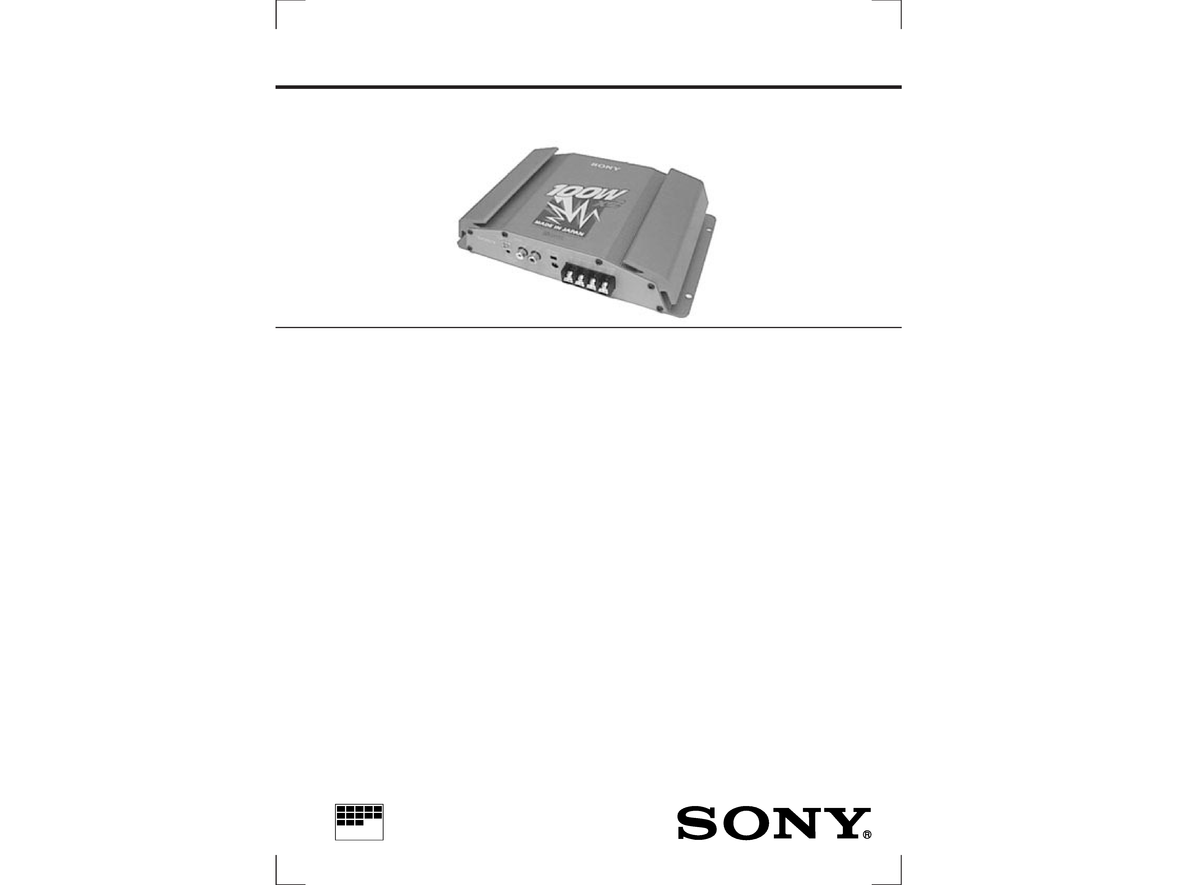
XM-222
SERVICE MANUAL
STEREO POWER AMPLIFIER
SPECIFICATIONS
E Model
Circuit system
OTL (output
transformerless) circuit
Pulse power supply
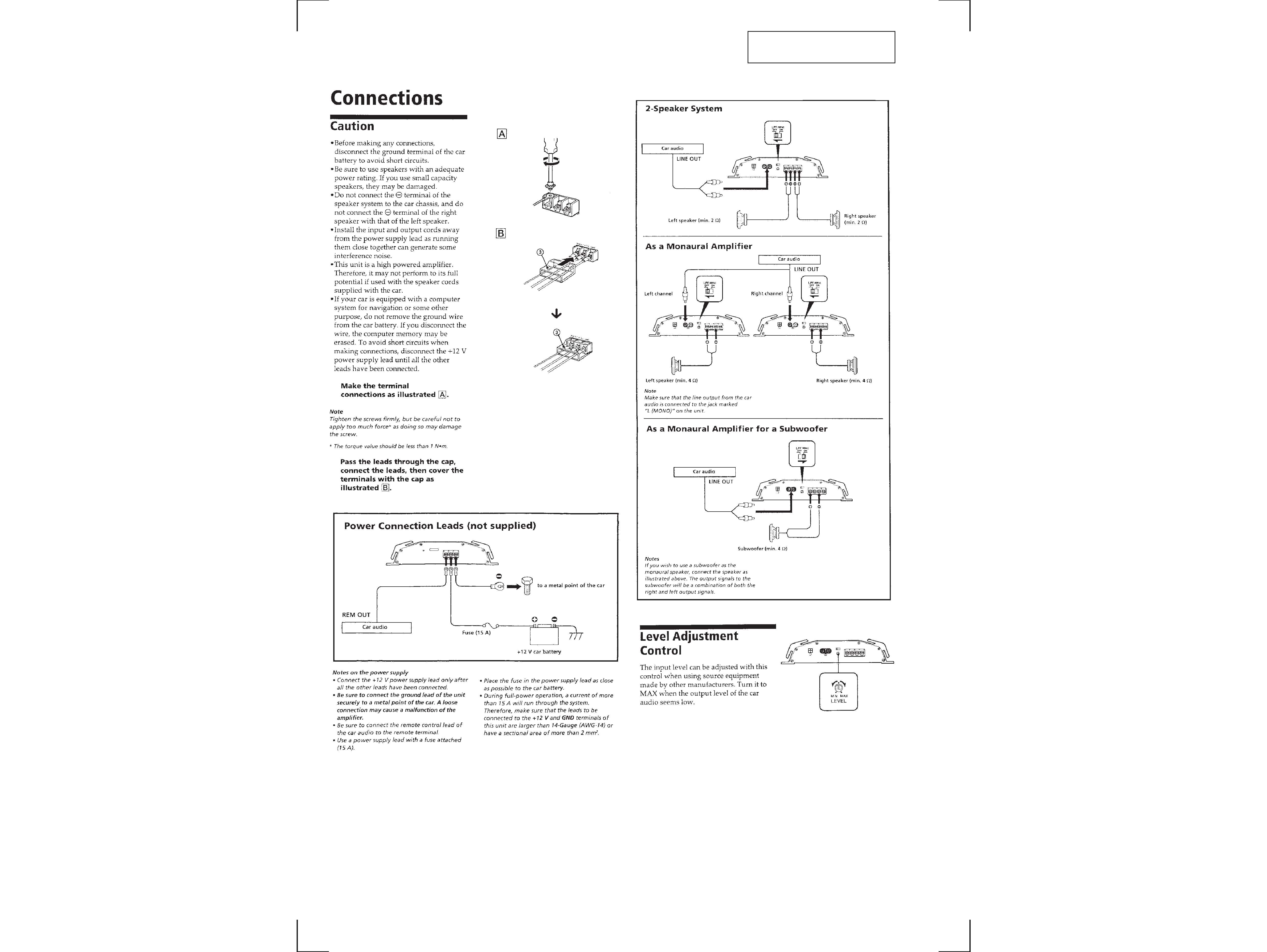
Inputs
RCA pin jacks
High level input
connector
Outputs
Speaker terminals
Speaker impedance
2 8 ohms (stereo)
4 8 ohms (when used as
a bridging amplifier)
Maximum output at 4 ohms
100 watts per channel
222 watts (monaural)
Rated output (supply voltage at 14.4 V)
35 watts per channel (20
Hz 20 kHz, 0.04 % THD,
at 4 ohms)
40 watts per channel (20
Hz 20 kHz, 0.1 % THD,
at 2 ohms)
Monaural: 80 watts (20
Hz 20kHz, 0.1 % THD,
at 4 ohms)
Frequency response
5Hz 80kHz (+0 dB)
-3
Harmonic distortion
0.005 % or less (at 1 kHz,
4 ohms, 10 watts)
Input level adjustment range
0.2 4V
Low-pass filter
80 Hz, 12 dB/oct
Power requirements
12 V DC car battery
(negative ground)
Power supply voltage
10.5 16V
Current drain
at rated output: 12 A (4
ohms, 35 watts x 2)
at 10% THD : 14A
Remote input: 1.5 mA
Dimensions
Approx. 230 x 53 x 145
mm (w/h/d) not incl.
projecting parts and
controls
Mass
Approx. 1.6 kg not incl.
accessories
Supplied accessories
Mounting screws (4)
High level input cord (1)
Protection cap (1)
Design and specifications are subject to change
without notice.
2
SECTION 1
GENERAL
This section is extracted from
instruction manual.
3
4
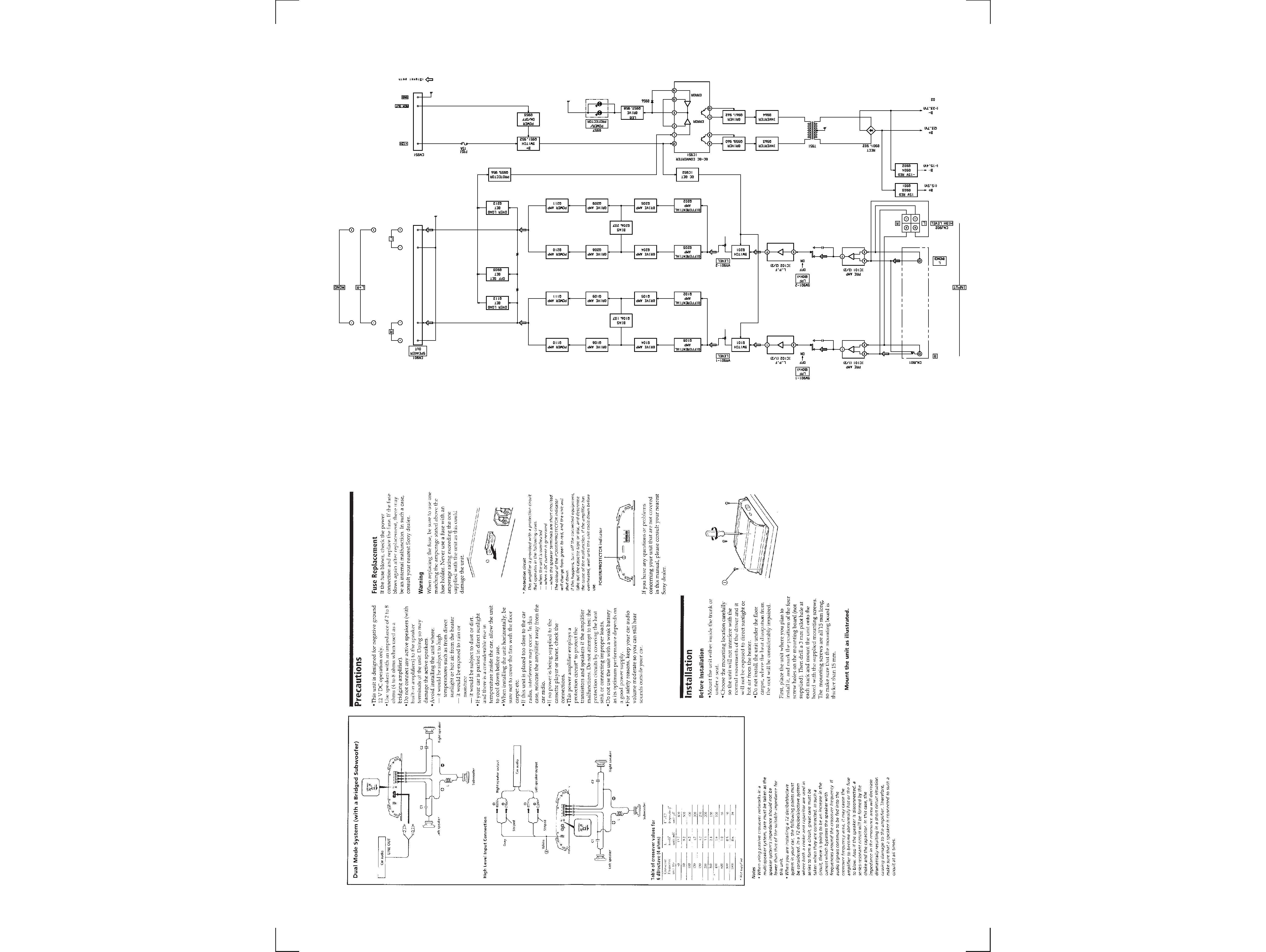
2-1. BLOCK DIAGRAM
SECTION 2
DIAGRAMS
XM-222
5
2-2. PRINTED WIRING BOARD
D101
F-4
D102
F-4
D201
F-8
D202
G-9
D901
A-6
D902
A-7
D903
C-10
D904
D-10
D951
D-4
D952
E-3
D953
D-7
D954
E-7
D955
D-7
D956
D-6
D957
B-2
IC101
H-10
IC102
F-9
IC951
C-6
IC952
E-6
Q101
E-10
Q102
G-4
Q103
G-4
Q104
G-4
Q105
G-5
Q106
I-4
Q107
I-4
Q108
H-4
Q109
H-5
Q110
I-3
Q111
I-5
Q112
G-3
Q201
G-10
Q202
G-8
Q203
F-8
Q204
G-7
Q205
G-8
Q206
I-8
Q207
I-8
Q208
H-7
Q209
H-8
Q210
I-7
Q211
I-9
Q212
G-2
Q901
D-10
Q902
D-10
Q903
B-10
Q951
D-4
Q952
D-4
Q953
H-2
Q954
E-6
Q955
E-4
Q956
E-6
Q957
C-2
Q958
C-2
Q959
C-2
Q960
B-2
Q961
B-2
Q962
C-6
Q963
A-4
Q964
A-5
Ref. No.
Location
r
Semiconductor
Location
Note:
· X : parts extracted from the component side.
· b : Pattern on the side which is seen.
XM-222
1
2
3
4
5
6
7
8
9
10
11
12
13
A
B
C
D
E
F
G
H
I
6
7
8
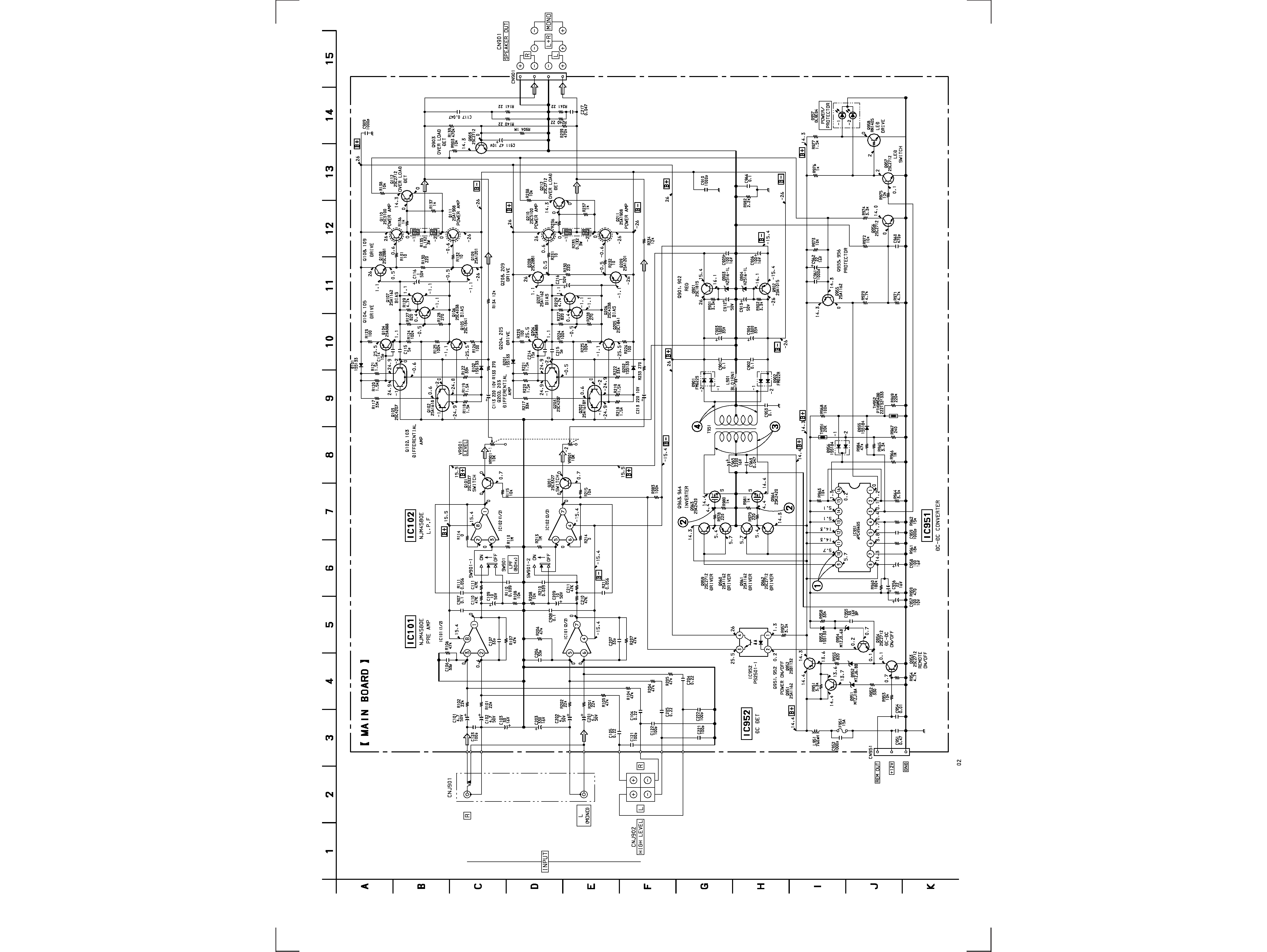
2-3. SCHEMATIC DIAGRAM
r
Refer to page 9 for Notes.
r
Refer to page 9 for IC Block Diagram. r Refer to page 9 for Wavforms.
XM-222