Conf
idential
SERVICE MANUAL
NOTEBOOK COMPUTER
9-874-583-05
For American Area
US Model
Lineup : PCG-NVR23
· Design and specifications are subject to
change without notice.
PCG-NVR23
S400
Ver 5-2005E
Revision History
-- 2 --
Information in this document is subject to change without notice.
Sony, VAIO and CLIE are trademarks or registered trademarks of
Sony. Microsoft, Windows, Windows Media, Outlook, Bookshelf
and other Microsoft products are trademarks or registered trademarks
of Microsoft Corporation in the United States and other countries.
The word Bluetooth and the Bluetooth logo are trademarks of
Bluetooth SIG, Inc. AMD, AMD logo, AMD Duron and
combinations thereof, 3DNow!, are trademarks of Advanced Micro
Devices, Inc. Intel Inside logo, Pentium and Celeron are trademarks
or registered trademarks of Intel Corporation. Transmeta, the
Transmeta logo, Crusoe Processor, the Crusoe logo and
combinations thereof are trademarks of Transmeta Corporation in
the USA and other countries. Graffiti, HotSync, PalmModem, and
Palm OS are resistered trademarks, and the Hotsync logo and Palm
are trademarks of Palm, Inc. or its subsidiaries. (M) and Motrola
are trademarks of Motrora, Inc. Other Motrola products and services
with (R) mark like Dragomball are the trademarks of Motrola, Inc.
All other names of systems, products and services in this manual
are trademarks or registered trademarks of their respective owners.
In this manual, the (TM) or (R) mark are not specified.
Service and Inspection Precautions
1. Obey precautionary markings and instructions
Labels and stamps on the cabinet, chassis, and components identify areas
requiring special precautions. Be sure to observe these precautions, as well
as all precautions listed in the operating manual and other associated
documents.
2. Use designated parts only
The set's components possess important safety characteristics, such as
noncombustibility and the ability to tolerate large voltages. Be sure that
replacement parts possess the same safety characteristics as the originals.
Also remember that the 0 mark, which appears in circuit diagrams and
parts lists, denotes components that have particularly important safety
functions; be extra sure to use only the designated components.
3. Always follow the original design when mounting
parts and routing wires
The original layout includes various safety features, such as inclusion of
insulating materials (tubes and tape) and the mounting of parts above the
printer board. In addition, internal wiring has been routed and clamped so
as to keep it away from hot or high-voltage parts. When mounting parts or
routing wires, therefore, be sure to duplicate the original layout.
4. Inspect after completing service
After servicing, inspect to make sure that all screws, components, and wiring
have been returned to their original condition. Also check the area around
the repair location to ensure that repair work has caused no damage, and
confirm safety.
5. When replacing chip components...
Never reuse components. Also remember that the negative side of tantalum
capacitors is easily damaged by heat.
6. When handling flexible print boards...
· The temperature of the soldering-iron tip should be about 270C.
· Do not apply the tip more than three times to the same pattern.
· Handle patterns with care; never apply force.
Caution: Remember that hard disk drives are easily damaged by
vibration. Always handle with care.
Caution Markings for Lithium/Ion Battery - The following or similar
texts shall be provided on battery pack of equipment or in both the
operating and the service instructions.
CAUTION: Danger of explosion if battery is incorrectly replaced.
Replace only with the same or equivalent type recommended by
the manufacturer. Discard used batteries according to the
manufacturer's instructions.
CAUTION: The battery pack used in this device may present a fire
or chemical burn hazard if mistreated. Do not disassemble, heat
above 100
°C (212°F) or incinerate.
Dispose of used battery promptly.
Keep away from children.
CAUTION: Changing the back up battery.
· Overcharging, short circuiting, reverse charging, multilation or
incineration of the cells must be avoided to prevent one or more of
the following occurrences; release of toxic materials, release of
hydrogen and/or oxygen gas, rise in surface temperature.
· If a cell has leaked or vented, it should be replaced immediately
while avoiding to touch it without any protection.
Confidential
PCG-NVR23 (AM)
-- 3 --
TABLE OF CONTENTS
CHAPTER 1. BLOCK DIAGRAM ............................... 1-1
(to 1-2)
CHAPTER 2. FRAME HARNESS DIAGRAM ........ 2-1
(to 2-2)
CHAPTER 3. EXPLODED VIEWS AND
PARTS LIST ............................................ 3-1
3-1. Main Section .................................................................... 3-3
3-2. LCD Section Made by TS ......................................... 3-7
3-3. Connector Section (CH Type only) ................................. 3-9
(to 3-10)
CHAPTER 4. OTHERS
4-1. Replacing the CPU .......................................................... 4-1
1. Removing the CPU .......................................................... 4-1
2. Installing the CPU ............................................................ 4-1
(to 4-1)
Section
Title
Page
Confidential
History of the changes is shown as the
"Revision History" at the end of this data.
PCG-NVR23 (AM)
Confidential
PCG-NVR23 (AM)
(END)
1-2
1-1
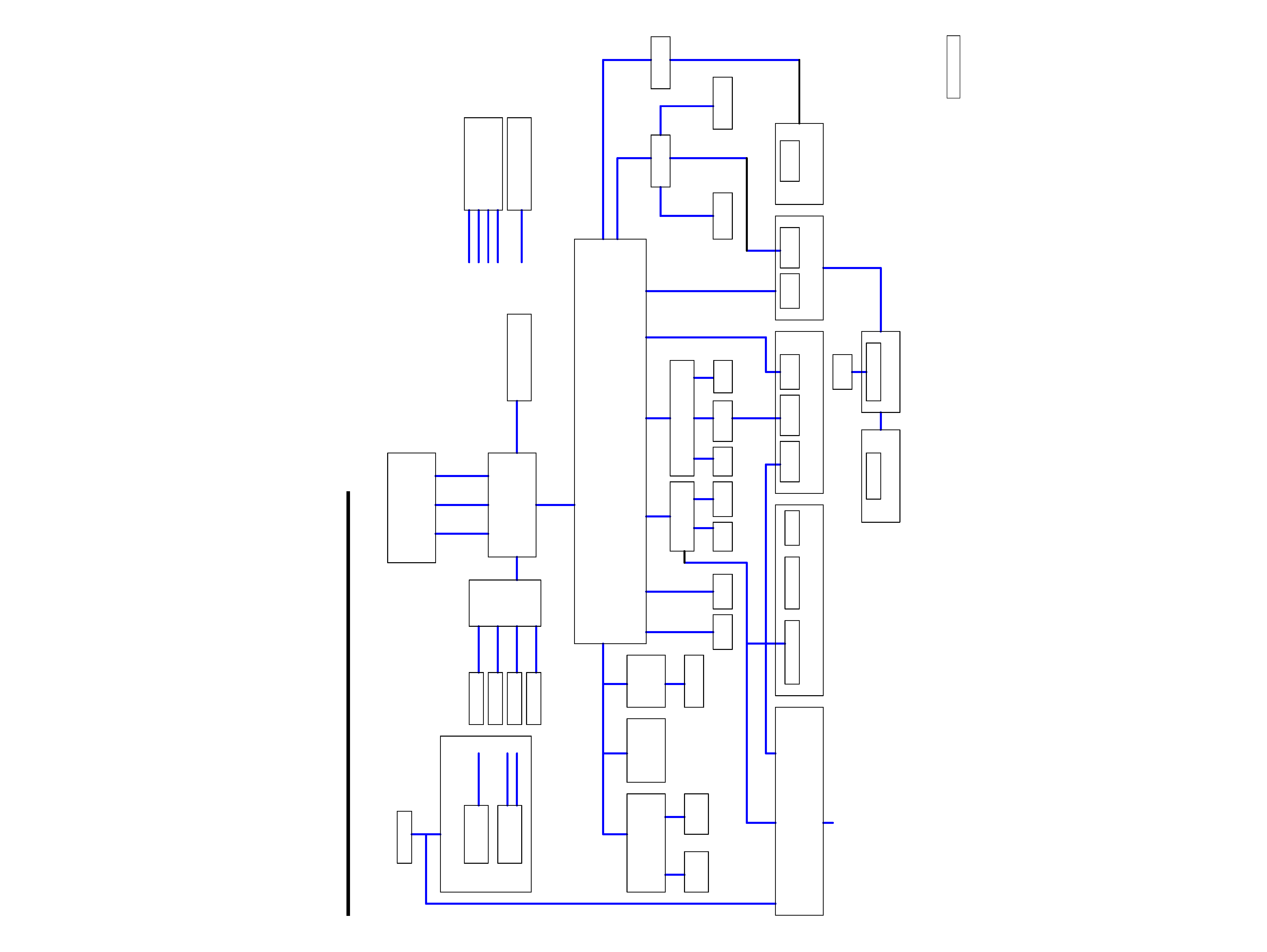
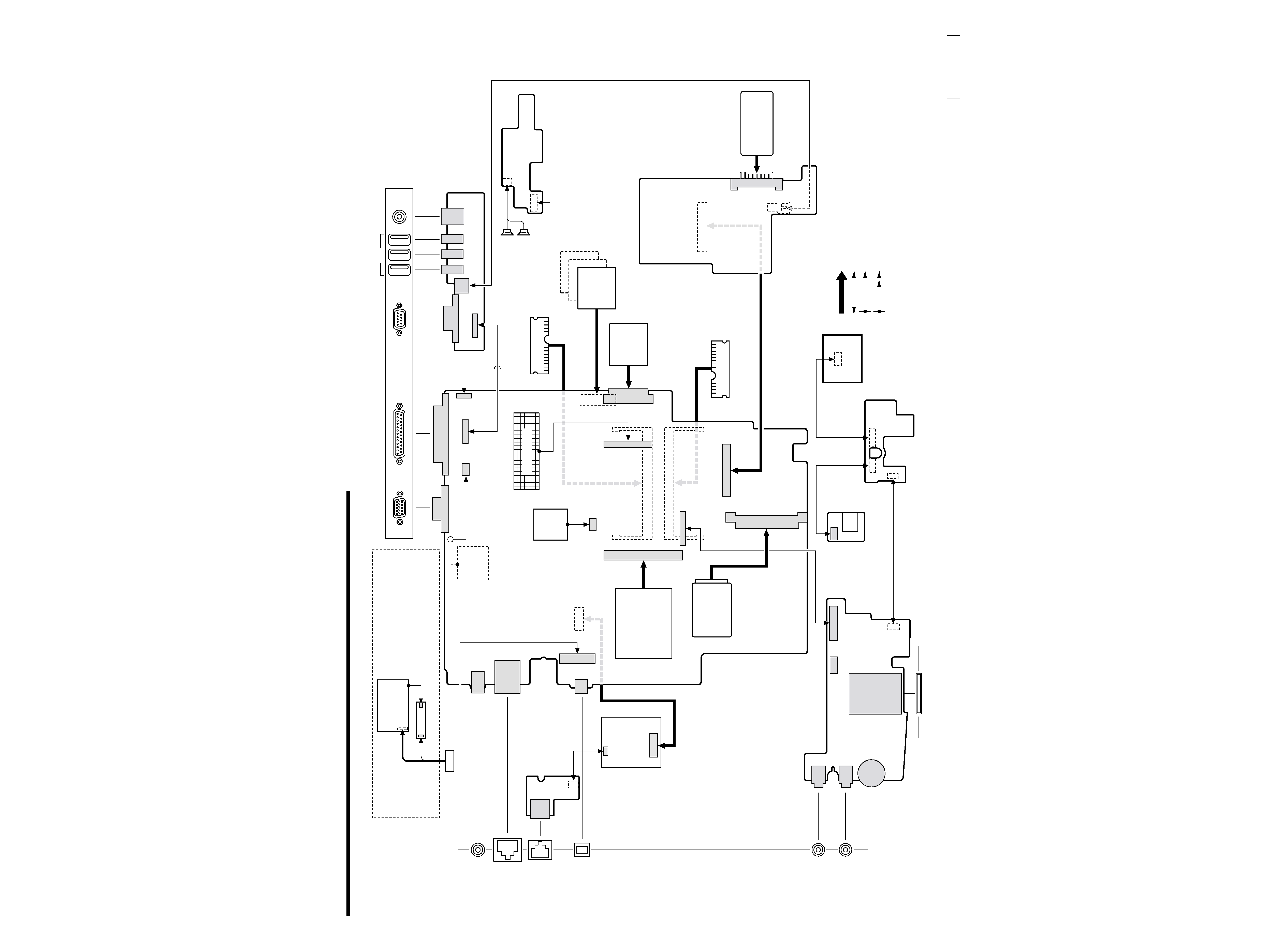
CHAPTER 1.
BLOCK DIAGRAM
Mini PCI
NS PC87391
I/O SUB BOARD
LVDS SIGNAL
INT.K/B
LPC
CPU CLOCK
PCU
Wirless LAN
SWX-98
USB
SIGNAL
AC
LINK1
POWER CIRCUIT
CPU-VCC_CORE
TPA0132
R/G/B
CDROM
BIOS
SWX-99
IFX-195
K/B LED
DDR VRAM
32MB
TV
MAX3243
DC JACK
POWER SWITCH BOARD
YMF753
NS PC87570
CNX-168
SWX-97
USB
SIGNAL*3
JOG SW BOARD
TV SIGNAL
AC
LINK2
DC/DC BOARD
INT.SPKR.
DRAM SIGNAL
HDD
XBUS
CNX-165
SUPER I/O
DC
JACK
RJ11 BOARD
AGP
POWER SWITCH
EXT.SPKR.
RJ11
RICOH 5C552
PRIMARY
IDE
BUS
PWX-19
MEMORY STICK
BOARD
EXT.MIC.
USB*3
NORTH BRIDGE
COM1
SLOT0/1
TOUCH
PAD
MOTHER BOARD
CTRL
SIGNAL
1394
462 PIN PGA
DDR
PCI CLOCK
BATTERY
SOUTH BRIDGE
VT82C33
SOCKET A
VLNK
SIGNAL
LPT
SECONDARY
IDE
BUS
MAXIM 1717
ICS93712
MBX-67
ADDRESS
RTL8100B
DDR CLOCK
JOG DIAL
USB CLOCK
LCD
MEMORY
STICK
Nvidia
Squish17
MAXIM 1632
PCI BUS
Realtek
RJ45
FDD
AMD
MDC
5V/5VSUS
DATA
CLOCK GENERATOR
ICS94228
CRT
KT266A-VT8366A
CLOCK BUFER
MOBILE ATHLON
T/P BOARD
T/P SWITCH
14M CLOCK
VIN
3V/3VSUS
SO-DIMM 1/2
CARDBUS+1394LINK/PHY
Confidential
PCG-NVR23 (AM)
(END)
2-2
2-1
CHAPTER 2.
FRAME HARNESS DIAGRAM
30
2
29
1
2
1
J1
CON2
21
CON2
CON1
2
1
40
39
CON7
CON9
CON4
CON21
CON8
CON6
26
25
2
1
CON19
26
25
2
1
CON4
13
CON1
77
1
154
78
40
39
2
1
CON18
CON10
2
25
1
24
CON16
39
40
1
2
PCN1
39
40
1
2
BCN1
CON15
CON2
CON1
CON3
CON6
CON7
1
2
BCN2
44
2
43
1
CON11
1
2
199
200
1
2
199
200
CON2
CON3
25
0
14
9
B21
A21
B1
A1
CON12
30
29
2
1
CON14
CON5
2
1
14
13
CON20
MBX-67 Board
(Side-A)
CNX-165 Board
(Side-A)
PWS-19 Board
(Side-A)
CNX-168 Board
(Side-A)
BCN3
18
CARD, MODEM
IFX-195 Board
(Side-A)
SWX-98 Board
(Side-A)
SWX-99 Board
(Side-A)
SWX-97 Board
(Side-A)
1
12
1
40
CN4001
CN4031
CN4011
CN4231
CN4201
BATTERY PACK
HARD DISK
10
1
11
0
CN4021
JP2
6
112
1
JP1
JP3
1
6
JP1
12
1
PAD, TOUCH
J1
1
14
CON
14
CON
PC CARD
CONNECTOR
DC FAN
13
CON15
DC FAN
KEY BOARD
From board to connector (direct connection)
Harness (connector at both end)
Harness (soldered at one end)
Connectors soldered on board and appearing on the panel
RAM
RAM
DDR266 SO-DIMM
SLOT A
DDR266 SO-DIMM
SLOT B
LCD HARNESS
INVERTER
LCD
LCD Block
OPTICAL
DEVICES
FLOPPY
DISK
DRIVE
Ten-Key
Woofer
SPEAKER
PHONE
PRINTER
MONTOR
NETWORK
IEEE 1394 i.LINK
EXTERNAL
MICROPHONE
HEADPHONE
SERIAL
USB
DC-IN
Rear Panel
L Side
Front Face
MEMORY STICK