SERVICE MANUAL
COLOR TELEVISION
BASIC CHASSIS
AC
No. 51757B
Jan. 2002
COPYRIGHT © 2002 VICTOR COMPANY OF JAPAN, LTD.
AV-27F802
AV-27F802 /AS
Supplementary
The following items for the AV-27F802/AS model were changed from those of the AV-
27F802 model.
Therefore, this service manual describes only the items which differ from those of the
AV-27F802 service manual.
For details other than those described in this manual, please refer the AV-27F802 serv-
ice manual (No. 51757, Sep., 2000).
Model No. & Parts No.
!
Ref. No.
AV-27F802
AV-27F802/AS
Parts Name
Remarks
(No. 51757)
(No. 51757B)
EXPLODED PARTS LIST (Page 34)
! T1502
QQH0084-001
QQH0119-001
FBT
Not Interchangeable
! V01
A68QCP891X001
A68QCP893X001
PICTURE TUBE
4
LC20217-004A-A
LC20217-004B-A
CONTROL KNOB
8
LC20269-001A-A
--
SP HOLDER
9
LC40317-001A
--
TAPPING SCREW
10
LC40226-001A
--
SPACER
12
QYSBSB4012Z
GQ40014-001A-A
TAPPING SCREW
Not Interchangeable
! 14
LC20626-001C-A
LC20626-001D-A
TERMINAL BOARD
! 17
LC10880-001C-A
LC10880-001D-A
REAR COVER
19
LC30684-005A-A
--
BBE LABEL
! 20
LC31139-001A-A
GQ30032-001A-A
RATING LABEL
Not Interchangeable
! 100
LC10878-001A-A
LC10878-001D-A
FRONT CABINET ASS'Y
101
LC20628-001A-A
LC202628-001B-A
DOOR
103
LC31238-001A-A
--
OPERATION SHEET
DIFFERENCE PARTS LIST
AV-27F802
2
No. 51757B
USING P. W. BOARD (Page 34)
Model No. & Parts No.
!
Ref. No.
AV-27F802
AV-27F802/AS
Parts Name
Remarks
(No. 51757)
(No. 51757B)
PACKING PARTS LIST (Page 43)
3
RM-C301G-1A
RM-C301G-2A
RC HAND UNIT
Interchangeable
! 6
LCT0821-001A-A
LCT0821-001D-A
INST BOOK
Not Interchangeable
7
LCT0822-001A-A
A68QCP893X001
SETUP GUIDE
9
BT-51020-1Q
BT-51028-1Q
REGISTRATION CARD
10
BT-20071B-Q
--
SVC CENTER LIST
PWB No. & Parts No.
! Symbol. No.
SAC-1501A-M2
SAC-1544A-M2
Parts Name
Remarks
MAIN PWB ASS'Y PARTS LIST (Page 36 39)
R1001
NRSA63J-333X
NRSA63J-473X
MG R
47kØ
1/16W
J
R1002
NRSA63J-102X
NRSA63J-0R0X
MG R
0.0Ø
1/16W ±0.5%
R1019
NRSA63J-104X
--
MG R
R1021
NRSA63J-333X
NRSA63J-123X
MG R
12kØ
1/16W
J
R1288
NRSA63J-271X
NRSA02J-471X
MG R
470Ø
1/10W
J
R1290
--
NRSA02J-561X
MG R
560Ø
1/10W
J
R1319
NRSA63J-101X
NRSA63J-102X
MG R
1kØ
1/16W
J
R1440
NRSA63J-101X
--
MG R
R1441
NRSA63J-103X
--
MG R
! R1535
NRVA02D-242X
NRVA02D-392X
MF R
3.9kØ
1/10W ±0.5%
R1536
--
NRVA02D-823X
MF R
82kØ
1/10W ±0.5%
R1711
NRSA63J-0R0X
--
MG R
R1739
NRSA63J-0R0X
NRSA63J-272X
MG R
2.7kØ
1/16W
J
R1744
NRSA63J-333X
--
MG R
R1755
NRSA63J-393X
NRSA63J-153X
MG R
15kØ
1/16W
J
R1775
NRSA63J-563X
NRSA63J-333X
MG R
33kØ
1/16W
J
R1776
NRSA63J-272X
NRSA63J-123X
MG R
12kØ
1/16W
J
R1818
--
NRSA63J-102X
MG R
1kØ
1/16W
J
C1043-44
NDC31HJ-390X
NDC31HJ-470X
C CAP.
47pF
50V
J
C1111
QETN0JM-108Z
QETN0JM-228Z
E CAP.
2200µF
6.3V
M
C1403
NCB21HK-393X
NCB21HK-153X
C CAP.
0.015µF
50V
K
! C1510
QFZ0196-402
QFZ0196-532
MPP CAP.
5300pF 1.5kVH
±3%
C1607
QETN1HM-106Z
QETN1HM-474Z
E CAP.
0.47µF
50V
M
MODEL
AV-27F802
AV-27F802/AS
ITEM
(No. 51757)
(No. 51757B)
MAIN PWB
SAC-1501A-M2
SAC-1544A-M2
DAF PWB
SAC-2601A-M2
--
CRT SOCKET PWB
SAC-3501A-M2
SAC-3514A-M2
FRONT PWB
SAC-8501A-M2
POWER SW PWB
SAC-8601A-M2
LF PWB
SAC-9501A-M2
PIP PWB
SAC0P501A-M2
AV SW PWB
SAC0S501A-M2
3D Y/C MODULE PWB
SAC-0Y501A
AV-27F802
No. 51757B
3
System Constant Setting (Page 9)
SPECIFIC SERVICE INSTRUCTION
YES
NO
Setting value
Setting item
Setting content
AV-27F802
AV-27F802/AS
CAN V-CHIP
NO
YES
PWB No. & Parts No.
! Symbol. No.
SAC-1501A-M2
SAC-1544A-M2
Parts Name
Remarks
C1708-09
NDC31HJ-330X
--
C CAP.
! T1502
QQH0084-001
QQH0119-001
FBT
L1024
QQL244K-220Z
--
PEAKING COIL
! L1521
QQLZ018-480
--
HEATER CHOKE
D1010
--
MTZJ9.1C-T2
ZENER DIODE
D1534
1S355-X
NRSA02J-0R0X
SI.DIODE/MG R
0.0Ø
1/10W
J
Q1440
2SC2412K/QR/-X
--
SI.TRANSISTOR
Q1706
2SC2412K/QR/-X
DTC363TK-X
SI.TRANSISTOR
IC1701
MN1876478JJ
MN186478JL1
I.C(MICRO-COMP)
IC1702
AT24C04-27F802
AT24C04-F802Y
I.C(MEMORY-OTH)
! FR1526
--
QRZ9013-R27
F R
0.27Ø
1/2W
K
PWB No. & Parts No.
! Symbol. No.
SAC-3501A-M2
SAC-3514A-M2
Parts Name
Remarks
R3119
NRSA63J-680X
NRSA63J-121X
MG R
120Ø
1/16W
J
C3301
NDC31HJ-471X
NDC31HJ-561X
C CAP.
560pF
50V
J
C3303
NDC31HJ-471X
NDC31HJ-561X
C CAP.
560pF
50V
J
C3331-33
NDC31HJ-561X
--
C CAP.
! SK3001
CE42670-001
QNZ0464-001
C.R.T.SOCKET
CRT SOCKET PWB ASS'Y PARTS LIST (Page 39 40)
AV-27F802
4
No. 51757B
Item
Measuring
instrument
Test point
Adjustment part
Description
MTS SAP
VCO
adjustment
Signal
generator
Frequency
counter
Remote
control unit
No.9 5FH MON.
No.10 SAP VCO
1. Receive a RF signal (non modulated sound signal) from the an-
tenna terminal.
2. Connect between pin 4 of [MPX] connector and GND (Pin 3 of [MPX]
connector) through 1MØ Resistor.
3. Select the No.9 5FH MON. of the SOUND MODE, and reset the
setting value from 0 to 1.
4. Connect the Frequency Counter to pin 2 of [MPX] connector and
GND (Pin 3 of [MPX] connector) .
5. Select the No.10 SAP VCO.
6. Set the initial setting value of the No.10 SAP VCO with the LEFT/
RIGHT key of the remote control unit.
7. Adjust the No.10 SAP VCO so that the frequency counter will dis-
play 78.67kHz±0.5kHz.
8. Select the No.9 5FH MON. of the SOUND MODE, and reset the
setting value from 1 to 0.
4 pin TP
3 pin GND
2 pin AUDIO_R
[MPX
Connector in
MAIN PWB]
MTS
SEPARATION
adjustment
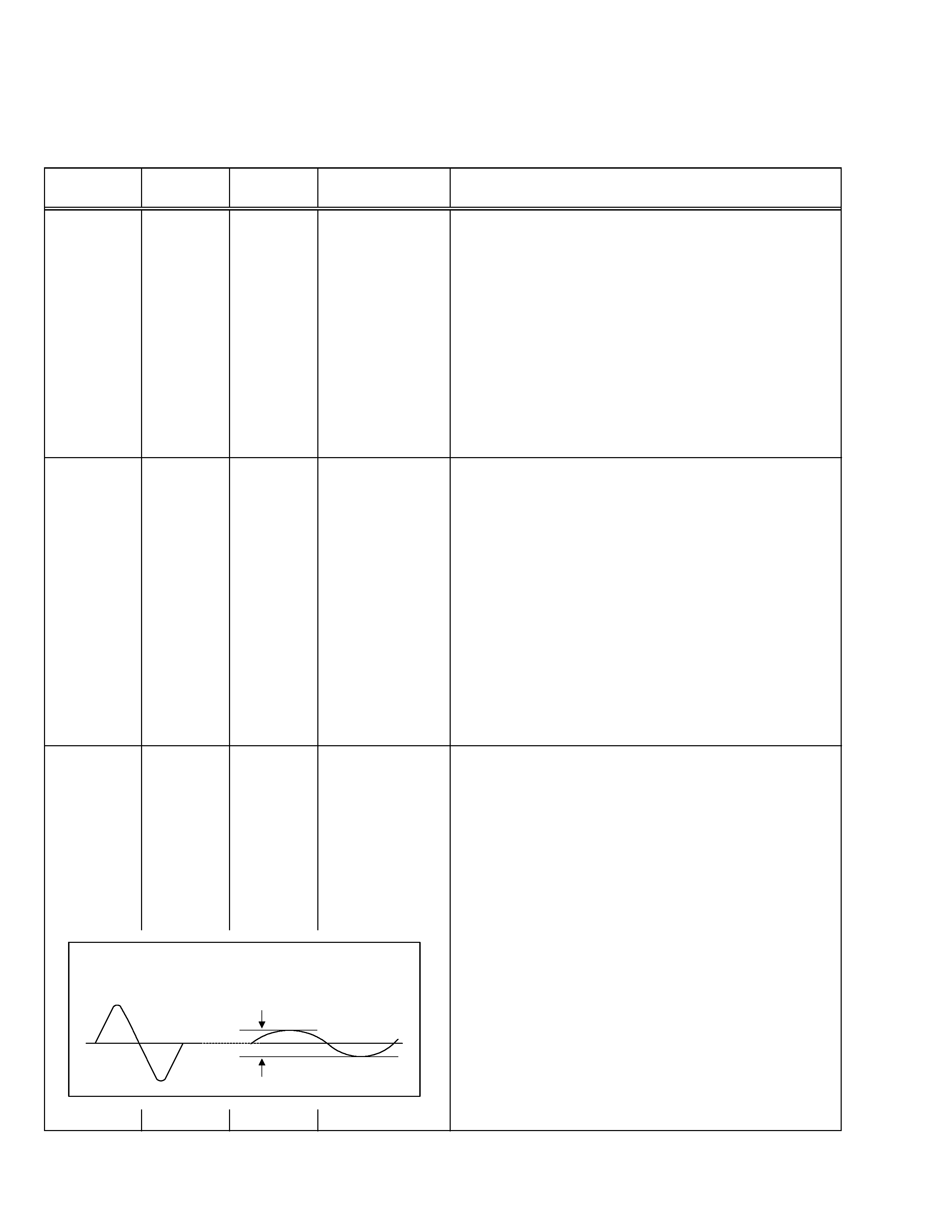
1. Input a stereo L signal (300Hz) from the TV audio multiplex signal
generator to the antenna terminal.
2. Connect an oscilloscope to pin 1 of [MPX] connector, and display
one cycle portion of the 300Hz signal.
3. Change the connection of the oscilloscope to pin 2 of [MPX] con-
nector, and enlarge the voltage axis.
4. Select the No.7 LOW SEP. of the SOUND MODE.
5. Set the initial setting value of the No.7 LOW SEP. with the LEFT/
RIGHT key of the remote control unit.
6. Adjust the No.7 LOW SEP. so that the 300Hz signal level will be-
come minimum.
7. Change the signal to 3kHz, and connect an oscilloscope to pin 1 of
[MPX] connector.
8. Adjust the No.8 HI SEP. so that the 3kHz signal level will become
minimum.
No.7 LOW SEP.
No.8 HI SEP.
TV audio
multiplex
signal
generator
Oscilloscope
Remote
control unit
1 pin AUDIO_L
2 pin AUDIO_R
3 pin GND
[MPX
Connector in
MAIN PWB]
L-Channel
signal waveform
R-Channel
crosstalk portion
Minimum
1 cycle
MTS STEREO
VCO
adjustment
Signal
generator
Frequency
counter
Remote
control unit
1. Receive a RF signal (nonmodulated sound signal) from the antenna
terminal.
2. Select the No.3 FH MONITOR of SOUND MODE, and change the
setting value from 0 to 1.
3. Connect the Frequency Counter to pin 2 of [MPX] connector and
GND (Pin 3 of [MPX] connector).
4. Select the No.4 STEREO VCO.
5. Set the initial setting value of the No.4 STEREO VCO with the LEFT/
RIGHT key of the remote control unit.
6. Adjust the No.4 STEREO VCO so that the frequency counter will
display 15.73kHz±0.1kHz.
7. Select the No.3 FH MONITOR of the SOUND MODE, and reset the
setting value from 1 to 0.
No.3 FH MONITOR
No.4 STEREO VCO
2 pin AUDIO R
3 pin GND
[MPX
Connector in
MAIN PWB]
SERVICE ADJUSTMENTS
ADJUSTMENTS
ADJUSTMENT OF MTS CIRCUIT (Page 29)
AV-27F802
No. 51757B
5
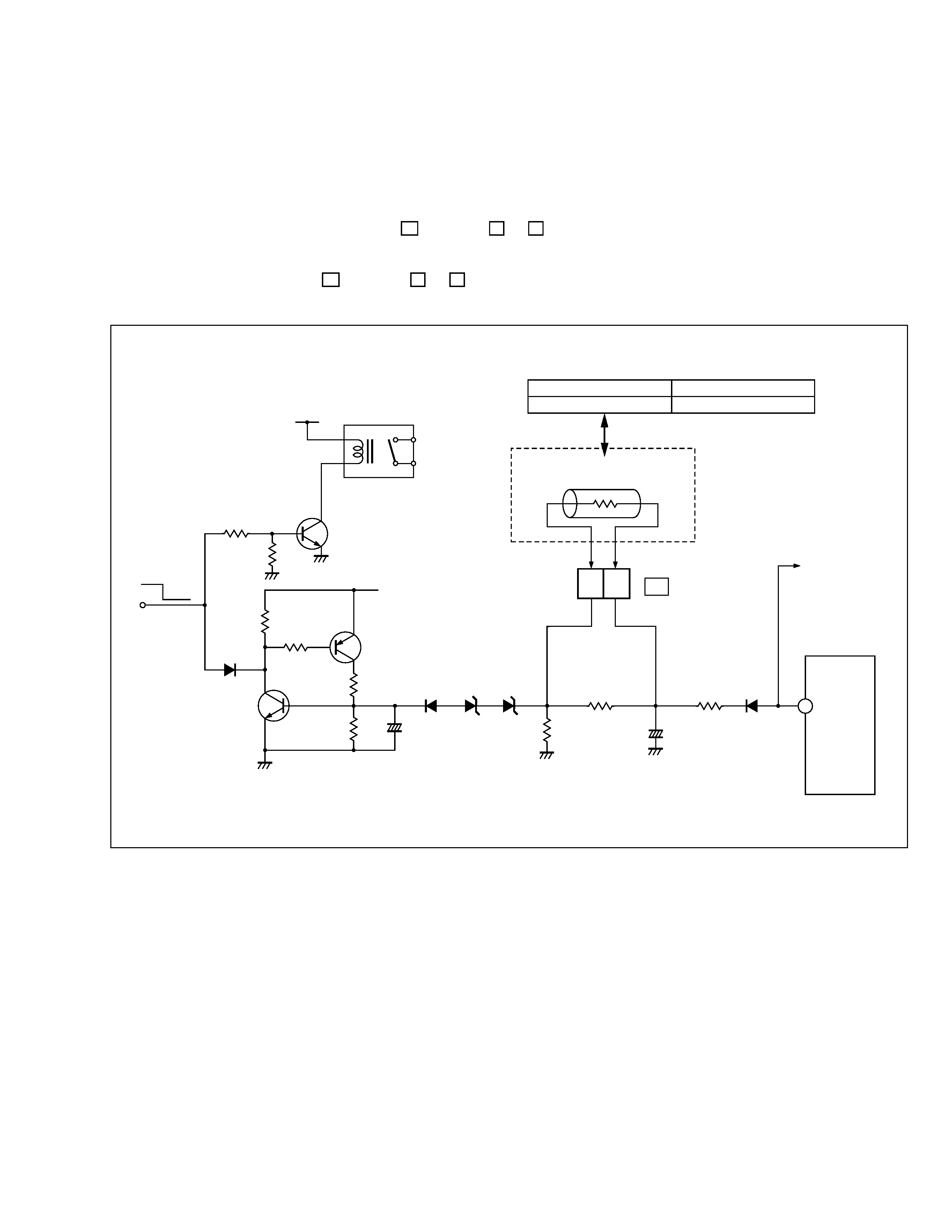
HOW TO CHECK THE HIGH VOLTAGE HOLD DOWN CIRCUIT (Page 30)
1. HIGH VOLTAGE HOLD DOWN CIRCUIT
After repairing the high voltage hold down circuit shown in Fig. 1.
This circuit shall be checked to operate correctly.
2. CHECKING OF THE HIGH VOLTAGE HOLD DOWN CIRCUIT
(1) Turn the POWER SW ON.
(2) As shown in Fig. 1, set the resistor (between S1 connector
2
&
3
).
(3) Make sure that the screen picture disappears.
(4) Temporarily unplug the power cord.
(5) Remove the resistor (between S1 connector
2
&
3
).
(6) Again plug the power cord, make sure that the normal picture is displayed on the screen.
Fig. 1
23
S1
CONNECTOR
HEATER
RESISTOR
+
+
POWER
ON OFF
RY951
R952
D535
R532
R951
Q951
Q532
Q531
R533
R534
R535
R538
C533
D534
D531
D532
BW
C525
R537
FR525
D525
T502
4
AV-27F802
20.66 kØ
± 103 Ø 1/4 W
AV-27F802/AS
15.0 kØ
± 75 Ø 1/4 W