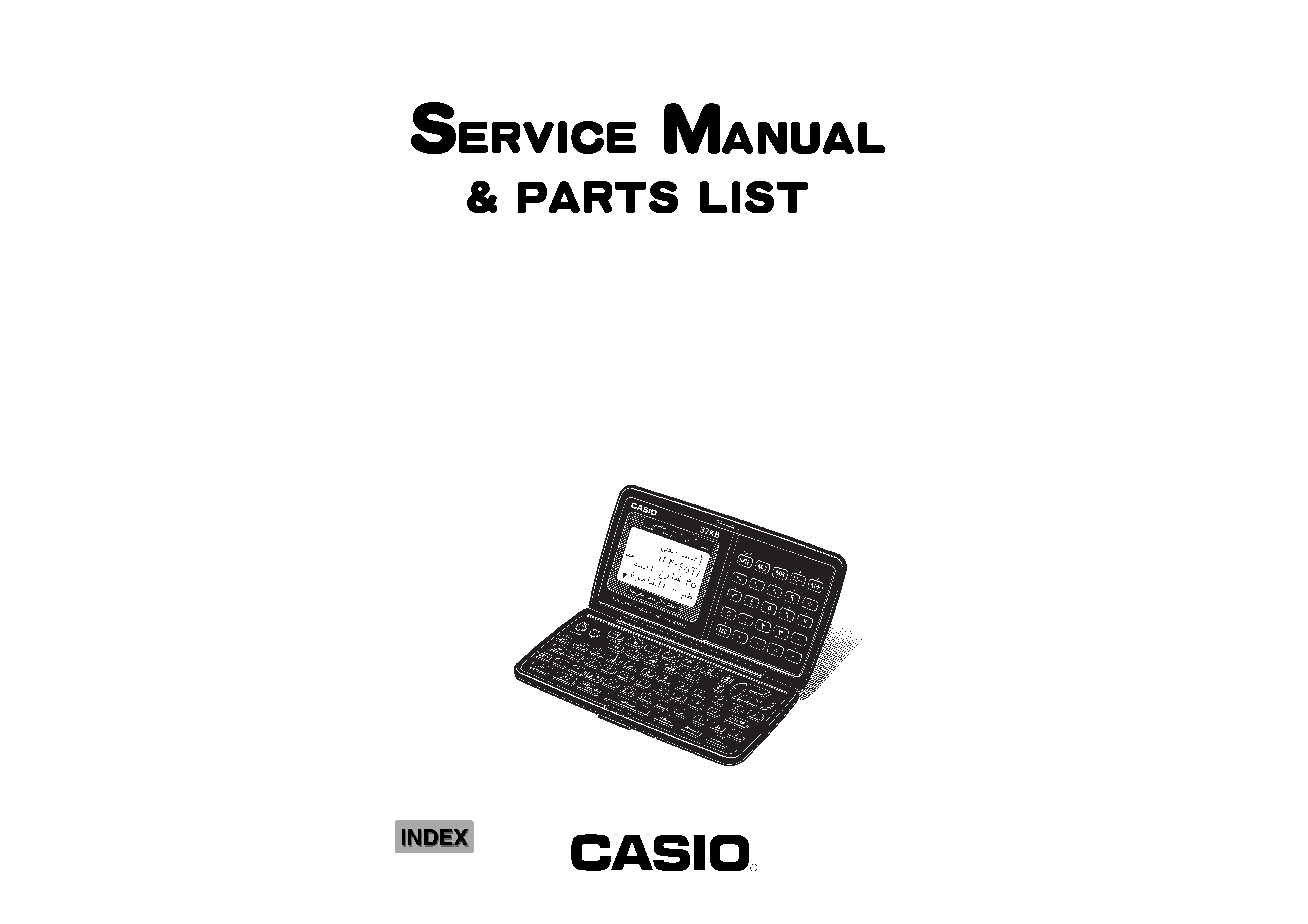
SF-5600AR(LX-589)
MAR. 1994
R
(with price)
SF-5600AR

CONTENTS
1.
SCHEMATIC DIAGRAM ................................................................................................ 1
2.
SPECIFICATIONS ......................................................................................................... 5
3.
TO REPLACE THE BATTERY ...................................................................................... 6
4.
TO CHECK THE MEMORY CAPACITY ........................................................................ 6
5.
ERROR MESSAGE ....................................................................................................... 7
6.
TO RESET THE DIGITAL DIARY ................................................................................. 8
7.
TO SAVE THE DATA TO OTHER MACHINE ............................................................... 9
8.
BLOCK DIAGRAM ...................................................................................................... 12
9.
CIRCUIT EXPLANATIONS
9-1.
System chart ................................................................................................. 13
9-2.
Power supply circuit .................................................................................... 14
9-3.
CPU pin description (HD62076C03) ............................................................ 17
9-4.
Gate array pin descriptions (SSC2571F0A) ............................................... 18
9-5.
Operation program ROM pin descriptions ................................................ 19
9-6.
RAM pin descriptions (M5M51008AFP-10LL) ............................................ 19
10.
DIAGNOSTIC OPERATION ........................................................................................ 20
11.
TROUBLESHOOTING................................................................................................. 25
12.
ASSEMBLY VIEW ....................................................................................................... 29
13.
PARTS LIST ................................................................................................................ 31
-- 1 --
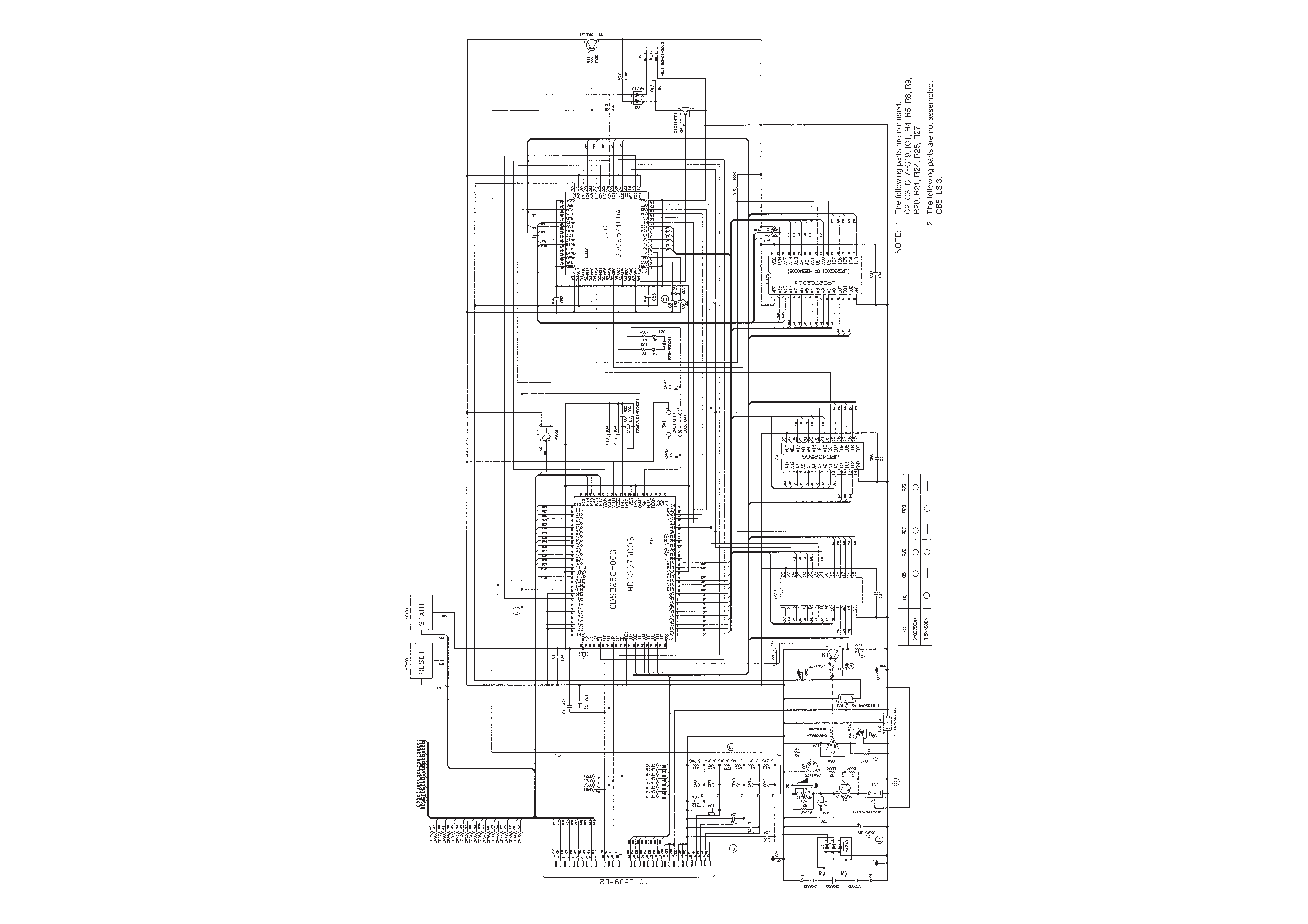
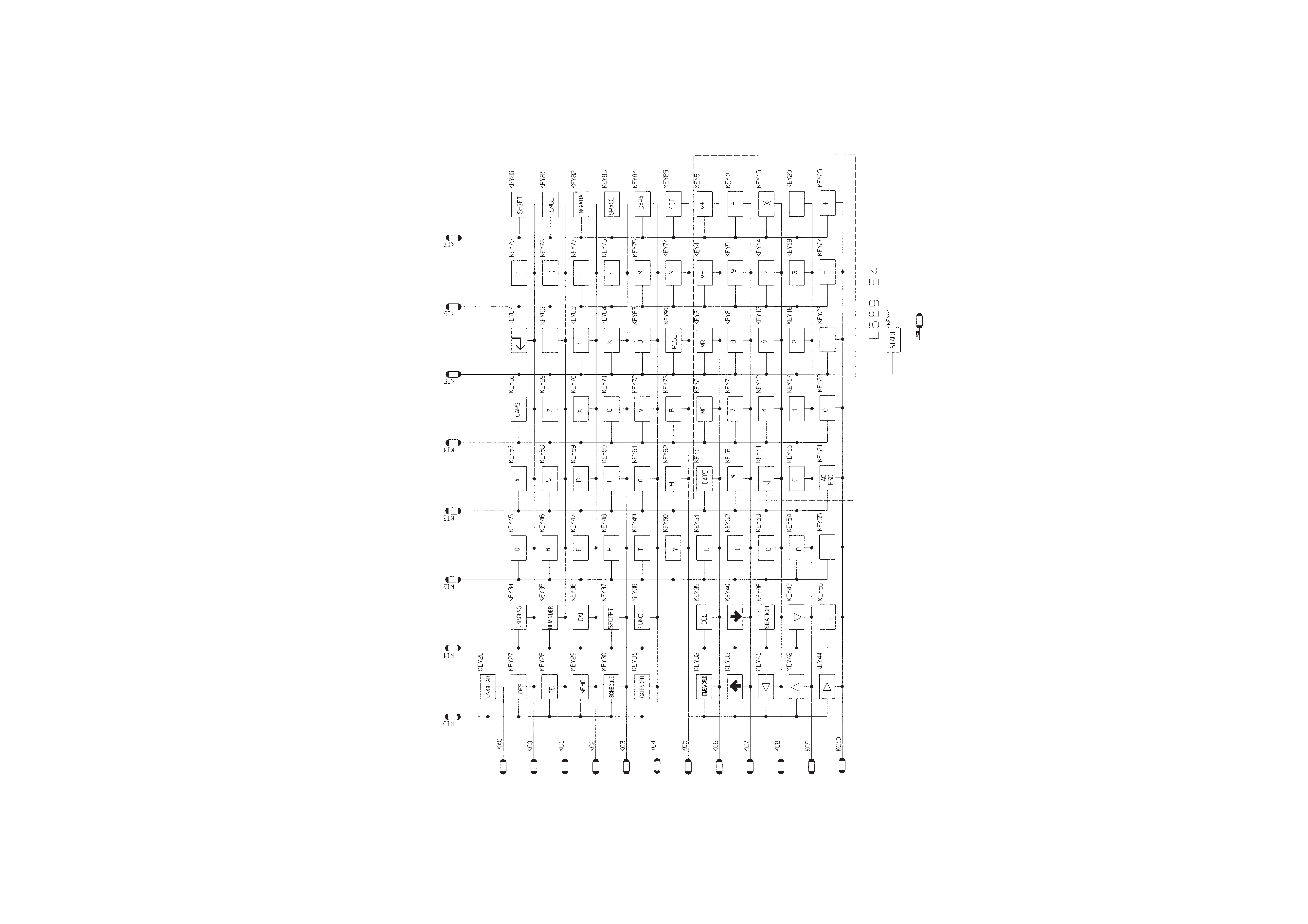
1.
SCHEMATIC DIAGRAM
1-1. Main PCB

-- 2 --
1-2. Display PCB
-- 3 --
1-3. Key Matrix