
CORDLESS TELEPHONE
SERVICE MANUAL
FILE NO. 2B0-200008
FT-8930
PUBLISHED IN JAPAN, Sep., 2000

1
1
CONTENTS
SAFETY PRECAUTIONS ............................................................................................................ 1
OPERATING CONTROLS ........................................................................................................... 2
ALIGNMENT PROCEDURE ........................................................................................................ 3
BLOCK DIAGRAMS ..................................................................................................................... 7
SCHEMATIC DIAGRAMS .......................................................................................................... 10
TROUBLESHOOTING HINTS ................................................................................................... 16
IC AND TRANSISTOR VOLTAGE CHART ............................................................................... 23
SEMICONDUCTOR LEAD IDENTIFICATION ........................................................................... 30
ELECTRICAL PARTS LOCATION ............................................................................................. 33
WIRING DIAGRAMS .................................................................................................................36
EXPLODED VIEW AND MECHANICAL PARTS LIST ............................................................... 39
PARTS LIST ............................................................................................................................... 43
ASSEMBLY PARTS LIST .......................................................................................................... 60
SPECIFICATIONS ..................................................................................................................... 61
SAFETY PRECAUTIONS
Before returning any models to the customer, a safety check of the entire instrument should be made.
The service technician must be sure that no protective device built into the instrument by the manufacture
has become defective or inadvertently degraded during servicing.
1.WARNING:
Alterations of the design or circuitry of these models should not be made.
Any design changes or additions such as, but not limited to, circuit modifications, auxiliary speaker
jacks, switches, grounding, active or passive circuitry, etc. may alter the safety characteristics of these
models and potentially create a hazardous situation for the user.
Any design alterations or additions will void the manufacturer's warranty and will further relieve the
manufacturer of responsibility for personal injury or property damage resulting therefrom.
2.PRODUCT SAFETY NOTICE
Many electrical and mechanical parts in this chassis have special characteristics. These characteristics
often pass unnoticed and the protection afforded by them cannot necessarily be obtained by using
replacement components rated for higher voltage, wattage, etc. Replacement parts that have these
special safety characteristics are identified in this manual and its supplements; electrical components
having such features are indentified by a
in the schematic diagram and the parts list. Before replacing
any of these components, read the parts list in this manual carefully. The use of substitute replacement
parts that do not have the same safety characteristics as specified in the parts list may create shock, fire
or other hazards.
2
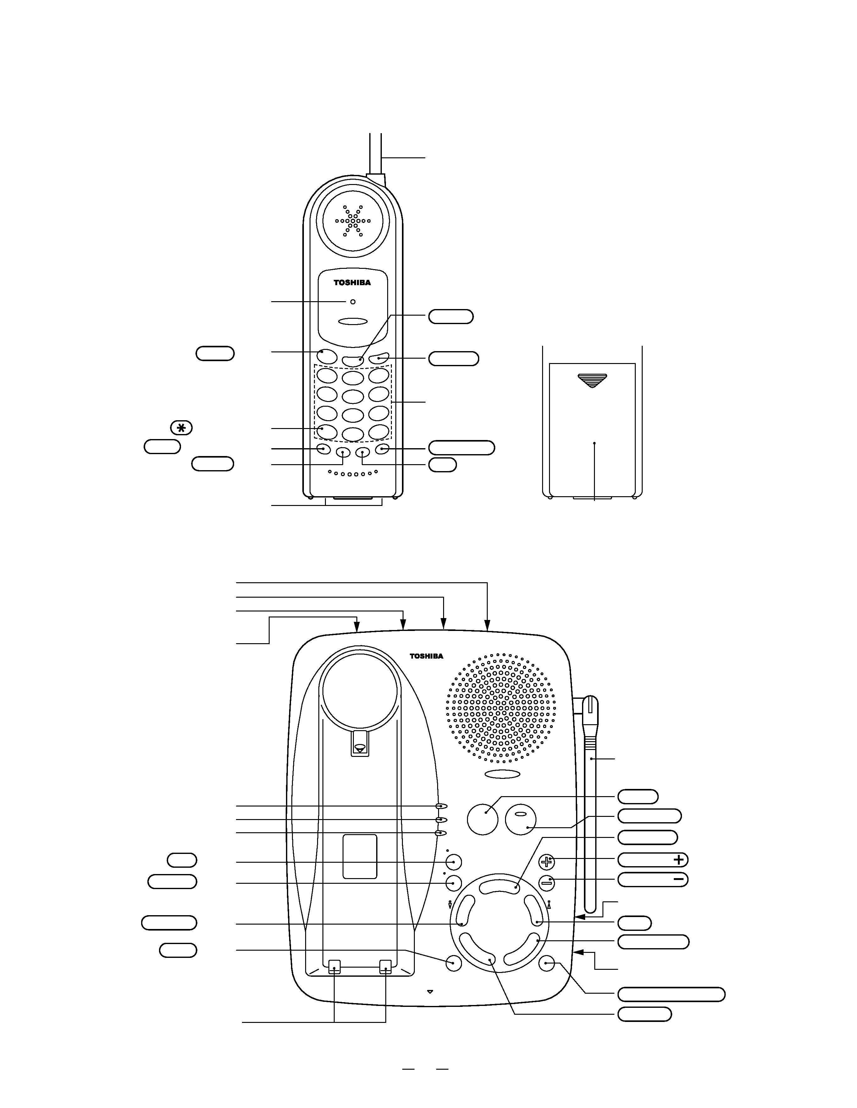
OPERATING CONTROLS
HANDSET CONTROLS AND FUNCTIONS
BASE UNIT CONTROLS AND FUNCTIONS
TALK Button
(TONE) Button
MEM (Memory) Button
MUTE Button
PIN Button
CLOCK Button
REPEAT Button
OGM Button
Charging contact
PULSE/TONE Switch
RINGER OFF-ON Switch
DC IN 9V Jack
TEL LINE Jack
Antenna
POWER
PAGE
SPEAKER
IN USE
CHARGE
PIN
CLOCK
OGM
MIC
MEMO
2WAY REC
VOLUME
CHARGE LED
IN USE LED
POWER LED
PAGE Button
SPEAKER Button
ANSWER Button
SKIP Button
PLAY/STOP Button
MEMO/2WAY REC Button
RING TIME Switch
(2 / 4 / TS)
REC TIME Switch
(ANN / 4 / 1)
DELETE Button
VOLUME
Button
VOLUME
Button
Charging Contact
VOL/RING Button
CH (channel)Button
Antenna
FLASH Button
RDL/P (Redial/Pause)Button
Dialpad
Rechargeable
Battery Pack(back)
TALK/BATT LOW LED
TALK
TALK
ABC
2
JKL
5
TUV
8
OPER
TONE
MEM
MUTE
CH
VOL/RING
RLD/P
FLASH
0
DEF
3
MNO
6
WX
YZ
PQ
RS
9
#
GHI
4
7
1
BATT LOW
COMPANDOR NOISE REDUCTION
900MHz
900MHz
R
E
P
E
A
T
ANSWER
S
K
IP
PLA
Y/
S
T
O
P
D
E
LE
TE
FT-8930
ALL DIGITAL ANSWERING SYSTEM
CORDLESS TELEPHONE
3
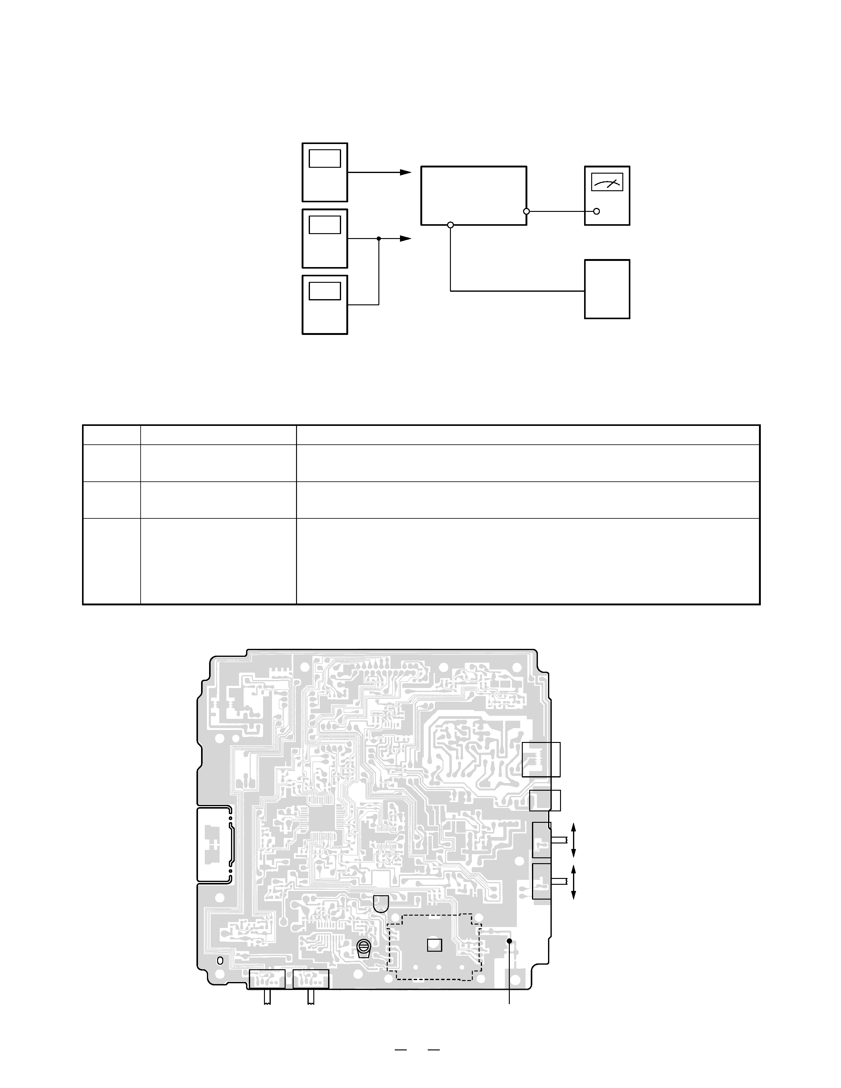
ALIGNMENT PROCEDURE
Base Unit
Transmitter Section
Connections
Preset
Press the "PAGE" key about 3.0 seconds while truning the power on.
Alignment Procedure
Alignment Point Location on Base Main PCB and Base RF PCB
step
1
2
3
Adjustment
RT301
(TX Power)
CT1
(TX Frequency)
RT3
(TX Modulation)
Remarks
Connect the Power Meter to the RF test point on the Base MAIN PCB.
Adjust RT301 for a -8.5dBm reading on the Power Meter.
Connect the Frequency Counter to the RF test point on the Base MAIN
PCB. Adjust CT1 to make sure that the frequency is 926.897468 MHz.
Press the "PAGE" key. Connect the AF Generator to the TEL Line Jack on
the Base Main PCB. Make sure that the output is 1 kHz -15dBm from the AF
Generator.
Connect the Deviation Meter to the RF test point on the Base MAIN PCB.
Adjust RT3 to indicate ±8 kHz Dev.
Base Main PCB
Power
Meter
RF
Test Point
BASE Unit
J4
DC IN
9V Jack
1kHz -15dBm
AF GEN.
AC 120V
60Hz
Frequency
Counter
Deviation
Mater
RF
Test Point
J1
TEL Line
Jack
AC
Adapter
RF Test Point
Base RF PCB
RT3
RT301
S4
J1
TEL LINE Jack
J4
DC IN 9V Jack
S1
PULSE/TONE Switch
TONE
PULSE
S3
CT1
S2
RINGER OFF-ON Switch
ON
OFF
4
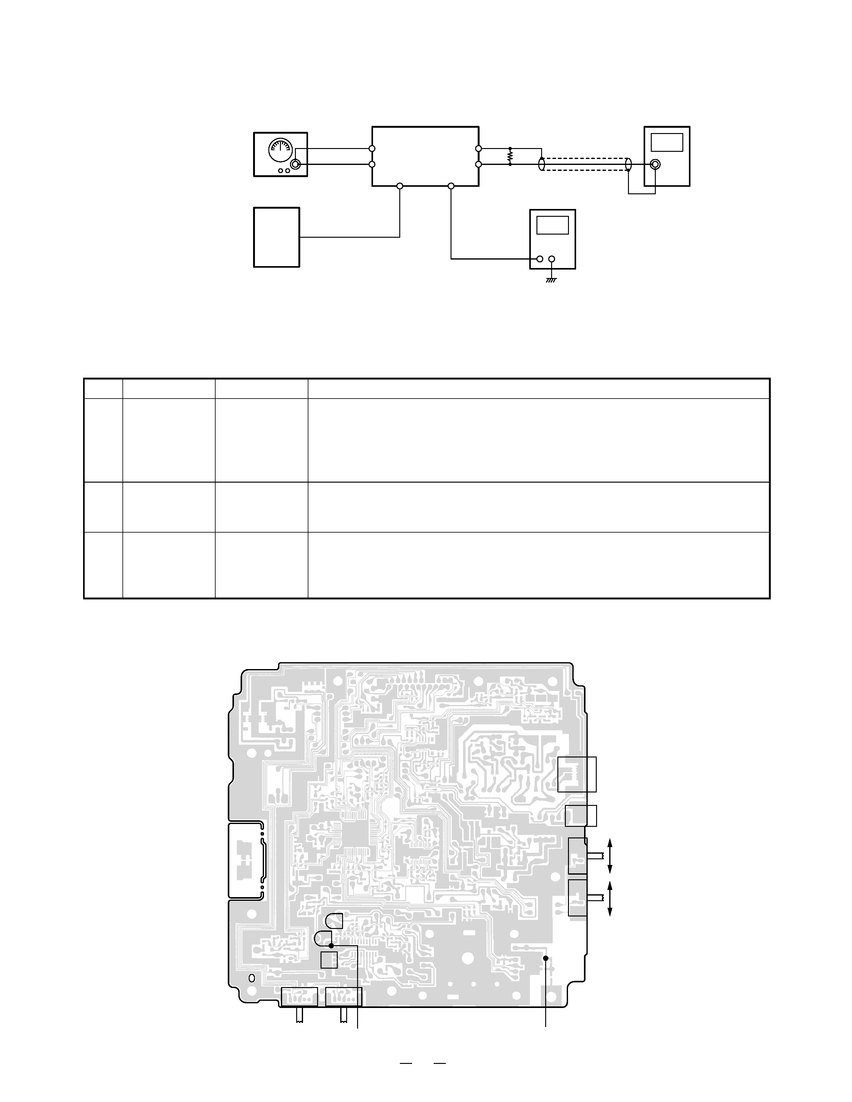
Receiver Section
Connections
Alignment Point Location on Base Main PCB and Base RF PCB
Preset
Place the Base Unit in RX SENS mode (step 4) in accordance with the precedure on page 3.
Alignment Procedure
step
1
2
3
Preset to
SG: 1mV
No modulation
SG: 1mV
1 kHz ±8kHz
deviation
SG: -113dB
µµµµµV
No modulation
Remarks
Connect the RF Signal Generator to the RF test point on the Base MAIN
PCB. Make sure that the frequency is 902.952467 MHz.
Connect the DC Voltmeter to the AF test point. Adjust L4 to indicate DC
1.00 V.
Connect the AC Voltmeter across a 600-ohm dummy to the Telephone Line
Jack. Adjust RT2 for a -11dBm reading on the AC voltmeter.
Press the "PAGE" key to enter the TEST Mode 5. Make sure that the
frequency of RF SG output is 902.952467 MHz. Adjust RT1 to turn to the
point where the LED indication is just vibrated.
Adjustment
L4
(Discriminator
Voltage)
RT2
(RX AF
Voltage)
RT1
(SQ Point)
AC Voltmeter
BASE Unit
AF
Test Point
Dummy Load
(600-ohm)
RF SG
AC 120V
60Hz
J4
DC IN 9V Jack
+
RF
Test Point
J1
TEL Line
Jack
AC
Adapter
DC Voltmeter
-
+
-
RF Test Point
Base Main PCB
AF Test Point
RT1
RT2
L4
S4
J1
TEL LINE Jack
J4
DC IN 9V Jack
S1
PULSE/TONE Switch
TONE
PULSE
S3
S2
RINGER OFF-ON Switch
ON
OFF