
CORDLESS TELEPHONE
SERVICE MANUAL
FILE NO. 2B0-9911
FD-9839
PUBLISHED IN JAPAN, Dec., 1999

1
CONTENTS
SAFETY PRECAUTIONS ............................................................................................................ 1
OPERATING CONTROLS ........................................................................................................... 2
ALIGNMENT PROCEDURE ........................................................................................................ 3
BLOCK DIAGRAMS ..................................................................................................................... 7
SCHEMATIC DIAGRAMS .......................................................................................................... 10
TROUBLESHOOTING HINTS ................................................................................................... 16
IC AND TRANSISTOR VOLTAGE CHART ............................................................................... 24
SEMICONDUCTOR LEAD IDENTIFICATION ........................................................................... 31
ELECTRICAL PARTS LOCATION ............................................................................................. 34
WIRING DIAGRAMS .................................................................................................................37
EXPLODED VIEW AND MECHANICAL PARTS LIST ............................................................... 40
PARTS LIST ............................................................................................................................... 44
ASSEMBLY PARTS LIST .......................................................................................................... 62
SPECIFICATIONS ..................................................................................................................... 63
SAFETY PRECAUTIONS
Before returning any models to the customer, a safety check of the entire instrument should be made.
The service technician must be sure that no protective device built into the instrument by the manufacture
has become defective or inadvertently degraded during servicing.
1.WARNING:
Alterations of the design or circuitry of these models should not be made.
Any design changes or additions such as, but not limited to, circuit modifications, auxiliary speaker
jacks, switches, grounding, active or passive circuitry, etc. may alter the safety characteristics of these
models and potentially create a hazardous situation for the user.
Any design alterations or additions will void the manufacturer's warranty and will further relieve the
manufacturer of responsibility for personal injury or property damage resulting therefrom.
2.PRODUCT SAFETY NOTICE
Many electrical and mechanical parts in this chassis have special characteristics. These characteristics
often pass unnoticed and the protection afforded by them cannot necessarily be obtained by using
replacement components rated for higher voltage, wattage, etc. Replacement parts that have these
special safety characteristics are identified in this manual and its supplements; electrical components
having such features are indentified by a
in the schematic diagram and the parts list. Before
replacing any of these components, read the parts list in this manual carefully. The use of substitute
replacement parts that do not have the same safety characteristics as specified in the parts list may
create shock, fire or other hazards.
2
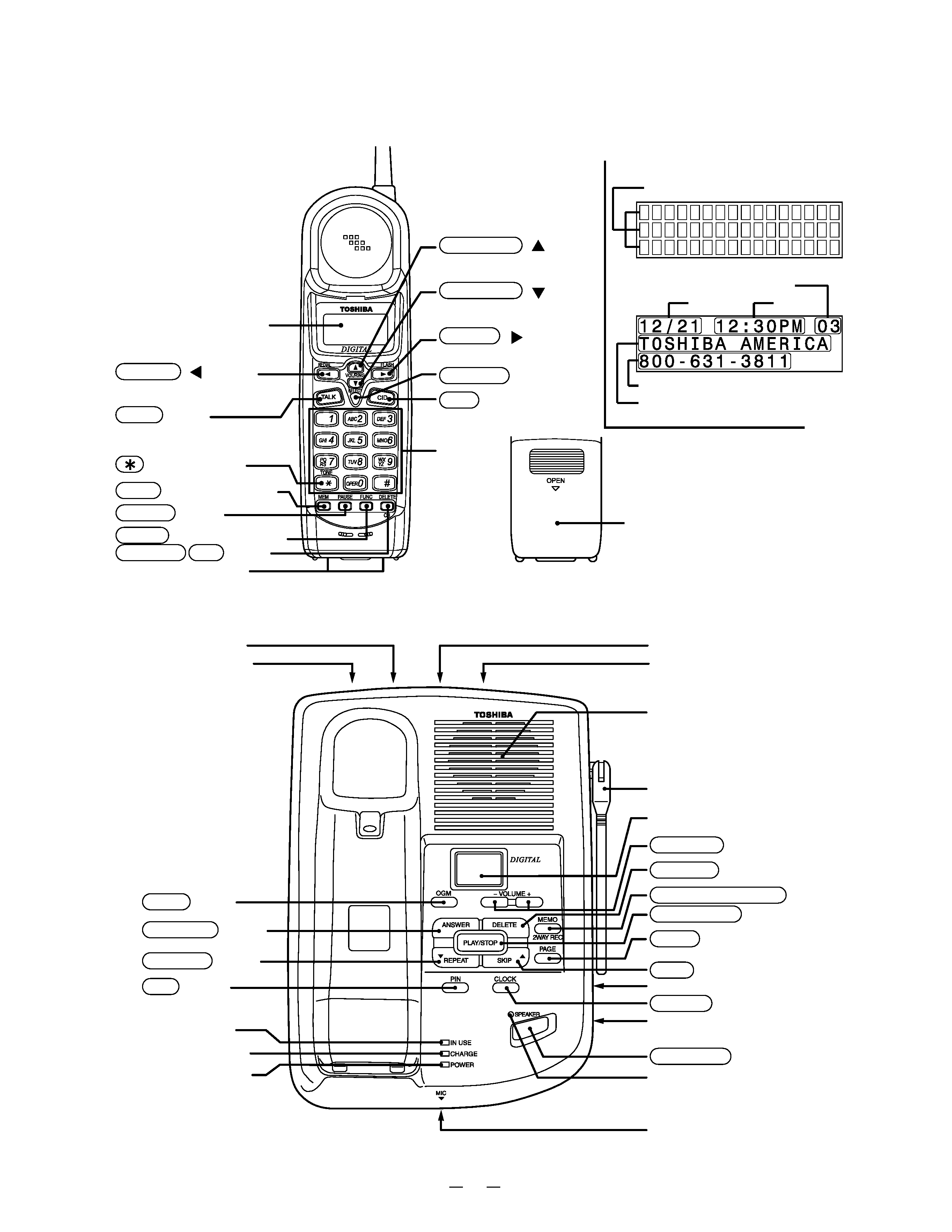
OPERATING CONTROLS
HANDSET CONTROLS AND FUNCTIONS
LCD
BASE UNIT CONTROLS AND FUNCTIONS
DC in 9V Jack
TEL LINE Jack
OGM button
ANSWER button
REPEAT button
PIN button
IN USE LED
CHARGE LED
POWERR LED
Liquid Crystal Display
(LCD)
REDIAL (
) button
(Left arrow button)
TALK button
PAUSE button
(TONE) button
MEM (Memory) button
FUNC (Function) button
DELETE
CH button
Charging contacts
VOL/RING (
) button
(up arrow button)
VOL/RING (
) button
(down arrow button)
FLASH (
) button
(Right arrow button)
SELECT button
T-P (TONE-PULSE) switch
Ringer ON/OFF switch
Speaker
Antenna
LED Display
VOLUME button
DELETE button
MEMO/2WAY REC button
PLAY/STOP button
PAGE button
SKIP button
Rec Time Switch (ANN/4/1)
CLOCK button
Ring Time Switch (2/4/TS)
SPEAKER button
Speaker LED
Microphone
CID (Caller ID) button
dialpad
Battery compartment
Dot matrix display
Number of calles
Date
Time
Caller's telephone number
Caller's name
900MHz
CALLER ID
FD-9839
3
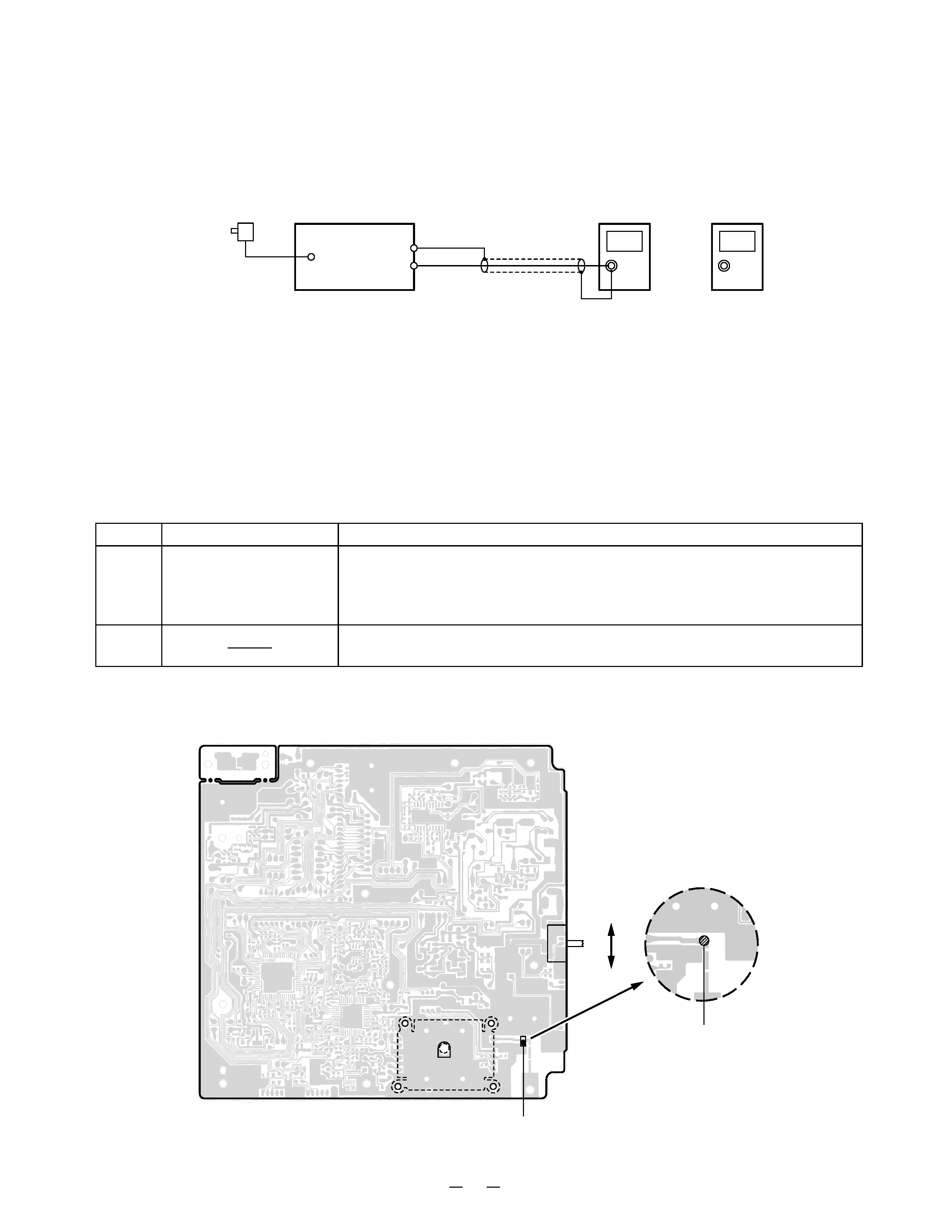
ALIGNMENT PROCEDURE
Base Unit
Transmitter Section
Connections
Alignment Point Location on Base Main PCB and Base RF PCB
step
1
2
Adjustment
VR202
(TX Power)
Remarks
Connect the Spectrum Analyzer to test point (J1).
Adjust VR202 so that the power instructions of the Spectrum analyzer reaches
-6.0dBm.
Then confirm the frequency is 926.295415 MHz.
Press the "PAGE" key twice and connect the FM Deviation Meter to test
point J1. Confirm the deviation is 23 ~ 46 kHz.
Base Main PCB
Test Point
Preset
a) Remove the solder on the pattern (refer to the illust. below).
b) Set the "TONE / PULSE" switch to PULSE.
c) Connect the AC adapter to the base unit while pressing the "PAGE" key, and keep pressing it continuously for
approximate 2 seconds.
d) Release the "PAGE" key when entering TEST mode 1 with CHARGE LED lighting.
Alignment Procedure
BASE Unit
Spectrum Analyzer
FM Deviation Meter
Test Point
(J1)
AC Adapter
(120V 60Hz)
S1
J1
Base RF PCB
Remove solder
before alignment
VR202
T
P
4
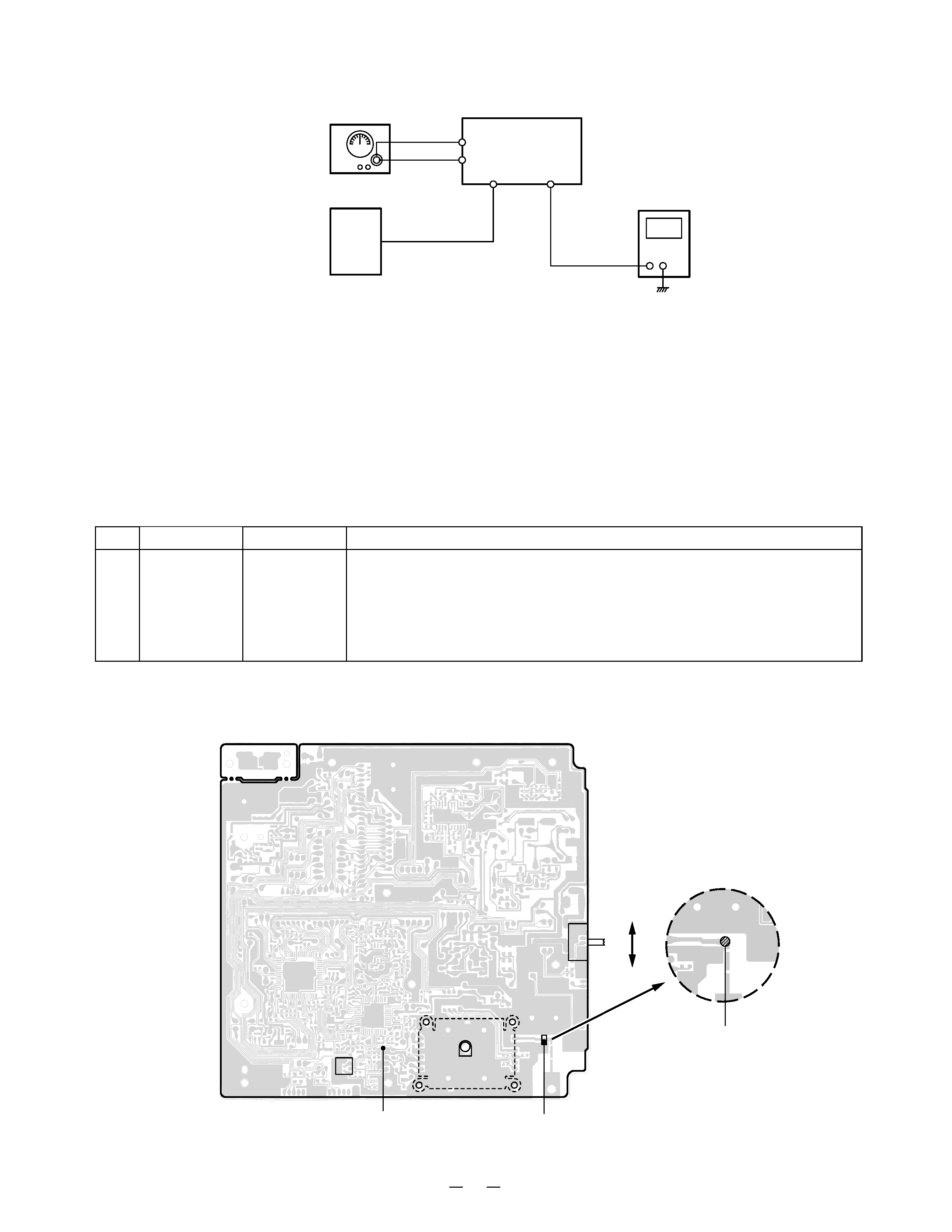
Receiver Section
Connections
Alignment Point Location on Base Main PCB and Base RF PCB
Preset
a) Remove the solder on the pattern (refer to the illust. below).
b) Set the "TONE/PULSE" switch to PULSE.
c) Connect the AC adapter to the base unit while pressing the "PAGE" key, and keep pressing it continuously for
approximate 2 seconds.
d) Release the "PAGE" key when entering TEST mode 1 with CHARGE LED lighting.
Alignment Procedure
step
1
Preset to
SG: 1mV
No modulation
Remarks
Press the "PAGE" key for 3 times to enter the TEST Mode 4. Connect the
RF Signal Generator to the test point (J1) on the Base MAIN PCB. Make
sure that the frequency is 903.417756 MHz.
Connect the DC Voltmeter to the Discriminator test point. Adjust L1 to
indicate DC 0.90 V.
Adjustment
L1
(Discriminator
Voltage)
Test Point
Base Main PCB
Discriminator Test Point
Test Point
(J1)
Discriminator
Test Point
DC IN
9V Jack
AC 120V
60Hz
BASE Unit
-
+
SG
DC Voltmeter
AC
Adapter
S1
J1
L1
Base RF PCB
Remove solder
before alignment
VR202
T
P