LCD TV
SERVICE MANUAL
FILE NO. 050-200224
15
DL72
DOCUMENT CREATED IN JAPAN, Oct., 2002
3-1
SAFETY PRECAUTION
WARNING: Service should not be attempted by anyone unfamiliar with the necessary precautions on this TV.
The following are the necessary precautions to be observed before servicing this chassis.
1. An isolation Transformer should be connected in the power line between the TV and the AC line before any
service is performed on the TV.
2. When replacing a chassis in the cabinet, always be certain that all the protective devices are put back in
place, such as; non-metallic control knobs, insulating covers, shields, isolation resistor-capacitor network
etc.
3. Before returning the set to the customer, always perform an AC leakage current check on the exposed
metallic parts of the cabinet, such as terminals, screwheads, metal overlays, control shafts etc. to be sure
the set is safe to operate without danger of electrical shock. Plug the AC line cord directly into a AC outlet
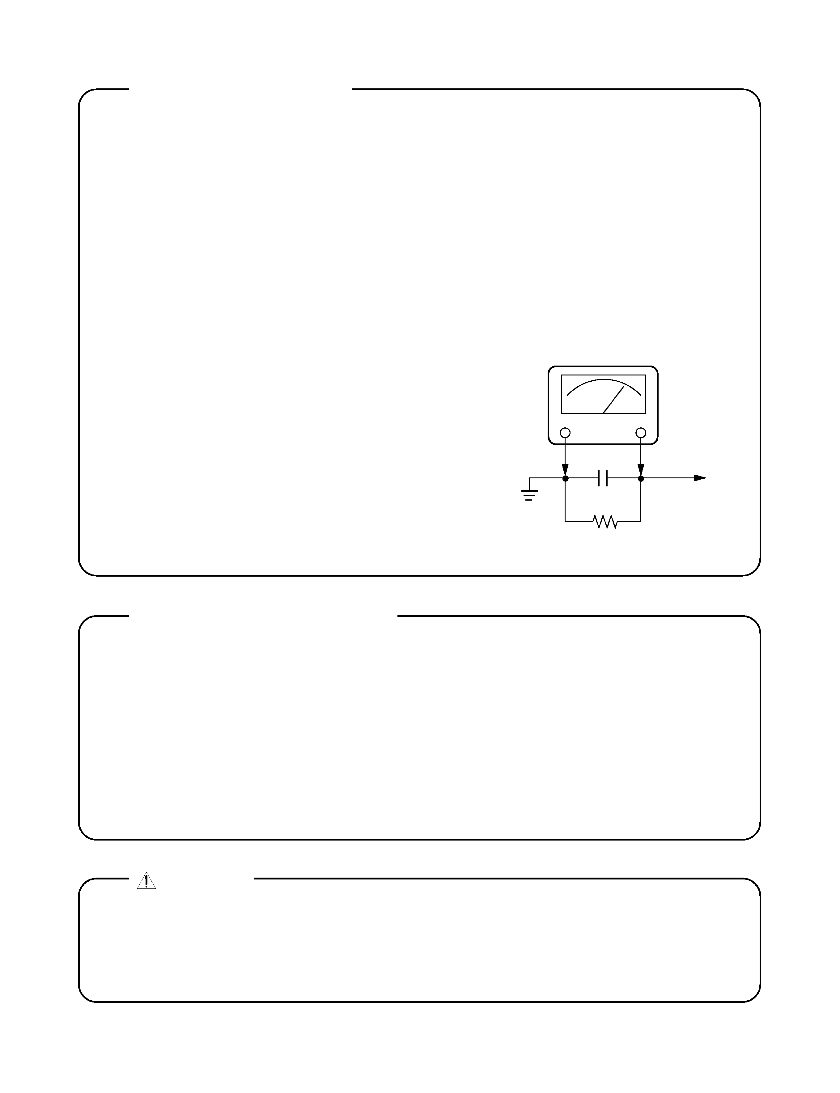
(do not use a line isolation transformer during this check). Use an AC voltmeter having 5000
W per volt or
more sensitivity in the following manner: Connect a 1500
W
10W resistor, paralleled by a 0.15
mF, AC type capacitor,
between a known good earth ground (water pipe, con-
duit, etc.) and the exposed metallic parts, one at a time.
Measure the AC voltage across the combination of 1500
W
resistor and 0.15
mF capacitor. Reverse the AC plug at
the AC outlet and repeat AC voltage measurements for
each exposed metallic part. Voltage measured must not
exceed 5.25V(rms). This corresponds to 3.5 mA(AC). Any
value exceeding this limit constitutes a potential shock
hazard and must be corrected immediately.
0.15
mF
1500
W
10W
Good earth ground
such as a water
pipe, conduit, etc.
Place this probe on
each exposed
metallic part.
AC VOLTMETER
PRODUCT SAFETY NOTICE
Many electrical and mechanical parts in this chassis have special safety-related characteristics. These charac-
teristics are often passed unnoticed by a visual inspection and the protection afforded by them cannot neces-
sarily be obtained by using replacement components rated for higher voltage, wattage, etc. Replacement parts
which have these special safety characteristics are identified in this manual and its supplements; electrical
components having such features are identified by the international hazard symbols on the schematic diagram
and the parts list.
Before replacing any of these components, read the parts list in this manual carefully. The use of substitute
replacement parts which do not have the same safety characteristics as specified in the parts list may create
shock, fire or other hazards.
DANGER
The components such as the power supply and FL inverter carry high voltages. When you partially disas-
semble the computer and turn on the components, use extreme care not to touch the connectors and compo-
nents to avoid the risk of electrical shock. Do not disassemble individual components during first-level mainte-
nance.
SAFETY NOTICE
Handling the LCD Module
Safety Precaution
In case the screen is damaged
and the internal liquid leaks, do
not suck or drink the internal
fluid. Nor do you touch it either,
otherwise you might be poisoned
or get a rash with your skin. If
the internal fluid enters your
mouth, rinse with water. If it
adheres to your skin or clothes,
wipe it away with alcohol and
then wash with water. If it enters
your eyes, wash with running
water immediately.
Precautions for handling the LCD module
The LCD module can be easily damaged during assembly
or disassembly. Observe the following precautions when
handling the LCD module:
1. When installing the LCD module in the LCD cover, be
sure to seat it so that it is properly aligned and
maximum visibility of the display is maintained.
2. Be careful to align the four holes at the right side and
left side of the LCD module with the corresponding
holes in the LCD cover before securing the module
with four screws. Do not force the module into place,
because stress can affect its performance. Also, the
panel's polarized surface is easily scarred, so be
careful when handling it.
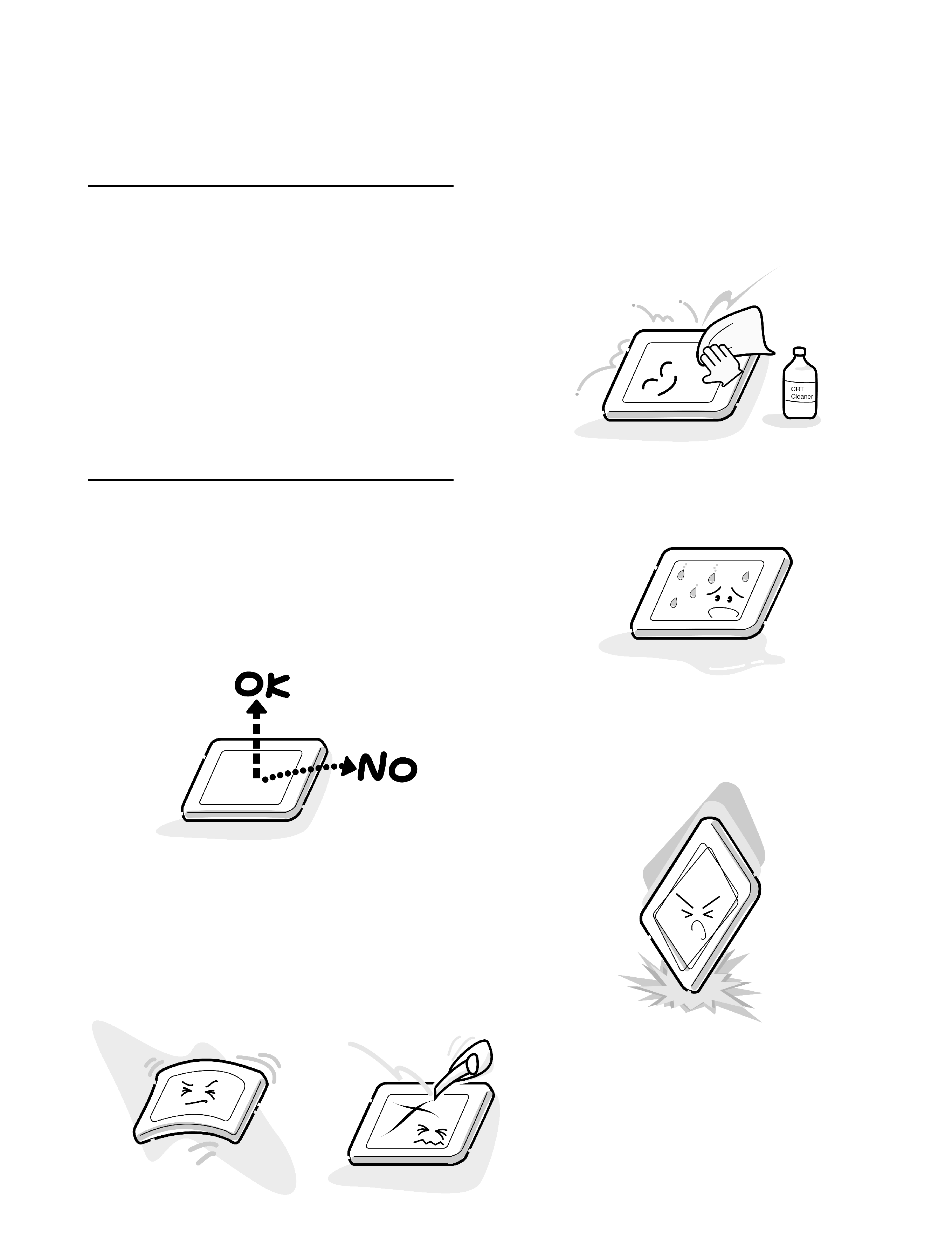
3. If the panel's surface gets dirty, wipe it with cotton or
a soft cloth. If it is still dirty, try breathing on the
surface to create a light condensate and wipe it again.
If the surface is very dirty, we recommend a CRT
cleaning agent. Apply the agent to a cloth and then
wipe the panel's surface. Do not apply cleanser
directly to the panel. Also, never scratch the surface.
4. If water or other liquid is left on the panel's surface for
a long period, it can change the screen's tint or stain it.
Be sure to quickly wipe off any liquid.
5. Glass is used in the panel, so be careful not to drop it
or let it strike a hard object, which could cause
breakage or cracks.
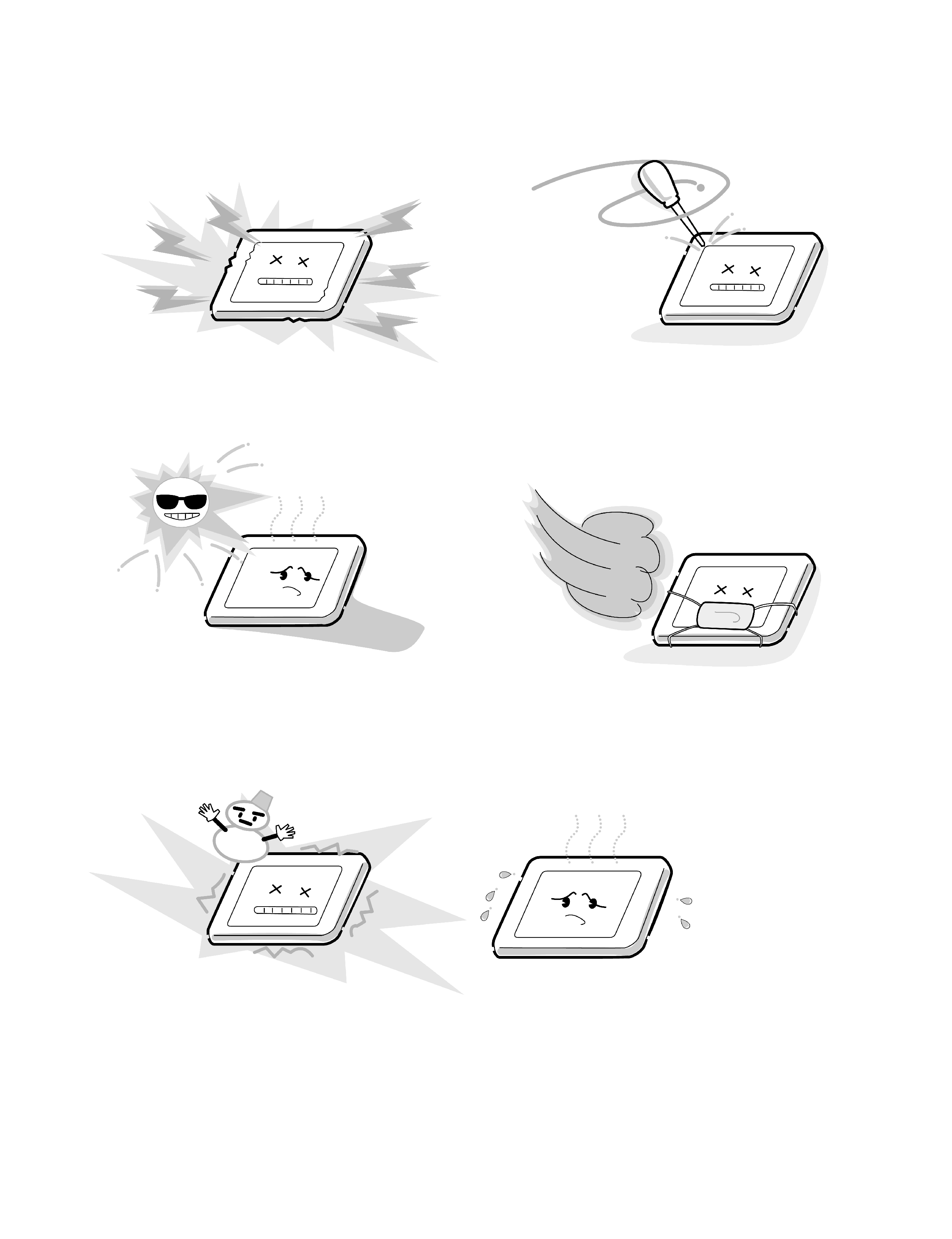
6. CMOS-LSI circuits are used in the module, so guard
against damage from electrostatic discharge. Be sure
to wear a wrist or ankle ground when handling the
module.
7. Do not expose the module to direct sunlight or strong
ultraviolet rays for long periods.
8. Do not store the module at temperatures below
specifications. Cold can cause the liquid crystals to
freeze, lose their elasticity or otherwise suffer damage.
9. Do not disassemble the LCD module. Disassembly can
cause malfunctions.
10. If you transport the module, do not use packing
material that contains epoxy resin (amine) or silicon
glue (alcohol or oxime). These materials can release
gas that can damage the panel's polarization.

SECTION 2
SERVICING DIAGRAMS
1. CIRCUIT SYMBOLS AND
SUPPLEMENTARY EXPLANATION ..................................... 2-1
1-1. Solid Resistor Indication ..................................................... 2-1
1-2. Inductor Indication ............................................................. 2-1
1-3. Capacitance Indication ....................................................... 2-1
1-4. Waveform and Voltage Measurement .............................. 2-1
1-5. Precautions for Part Replacement ..................................... 2-1
2. BLOCK DIAGRAMS .................................................................. 2-2
2-1. Power Block Diagram ......................................................... 2-2
2-2. Inverter Block Diagram ...................................................... 2-3
2-2-1. Pin Assignments (microprocessor) IC701: KS88C6348 ... 2-4
2-3. Main Block Diagram ........................................................... 2-5
3. CIRCUIT DIAGRAMS ............................................................... 2-7
3-1. Power Supply Circuit Diagram .......................................... 2-7
3-2. Microprocessor Circuit Diagram ....................................... 2-9
SECTION 3
PARTS LIST
SAFETY PRECAUTION ................................................................. 3-1
NOTICE ............................................................................................. 3-1
ABBREVIATIONS ........................................................................... 3-1
1. Integrated Circuit (IC) ............................................................ 3-1
2. Capacitor (Cap) ....................................................................... 3-1
3. Resistor (Res) ........................................................................... 3-1
CONTENTS
SECTION 1
ADJUSTMENT PROCEDURES AND PART REPLACEMENT
1. REMOVAL .................................................................................. 1-1
1-1. Front Panel .......................................................................... 1-1
1-2. LCD Panel ............................................................................ 1-1
1-3. Inverter PC Board ............................................................... 1-2
1-4. Sensor PC Board ................................................................. 1-3
1-5. Handle .................................................................................. 1-3
1-6. LCD Rear Cover ................................................................. 1-3
1-7. Wall Hanging Plate ............................................................. 1-4
1-8. Bottom Cover ....................................................................... 1-4
1-9. Side Cover ............................................................................ 1-4
1-10.Rear Terminal Panel, Main PC Board .............................. 1-4
1-11.Front Net, Speaker .............................................................. 1-5
1-12.Switch PC Board ................................................................. 1-5
1-13.Hinge, Top Cover ................................................................ 1-5
3-3. Input Jack Circuit Diagram ............................................. 2-11
3-4. VPC3230 Circuit Diagram ............................................... 2-13
3-5. TTX&Caption Circuit Diagram ...................................... 2-15
3-6. MXIC Circuit Diagram .................................................... 2-17
3-7. Frame Buffer Circuit Diagram ........................................ 2-19
3-8. Panel Interface Circuit Diagram ..................................... 2-21
3-9. Sound Circuit Diagram ..................................................... 2-23
3-10.Wow Control Circuit Diagram ........................................ 2-25
3-11.Sound Amplifier Circuit Diagram ................................... 2-27
3-12.Pin Voltage ......................................................................... 2-29
3-13.Waveforms ......................................................................... 2-36
4. PC BOARDS .............................................................................. 2-41
4-1. Main PC Board .................................................................. 2-41
4-2. Switch PC Board ............................................................... 2-45
4-3. Sensor PC Board ............................................................... 2-45
2. GND LEAD WIRE CONNECTION DIAGRAM .................... 1-6
3. LOCATION OF MAIN PARTS ................................................. 1-7
4. TROUBLESHOOTING .............................................................. 1-8
4-1. No Power (No Video & No Sound) .................................... 1-8
4-2. No Video ............................................................................... 1-9
4-2-1. No Video (Sound O.K) .................................................... 1-9
4-2-2. No Video (Sound O.K) .................................................... 1-9
4-3. No Sound (Video O.K) ...................................................... 1-10
4. EXPLODED VIEWS ................................................................... 3-2
4-1. Packing Assembly ................................................................ 3-2
4-2. Chassis Assembly ................................................................ 3-3
5. PARTS LIST ................................................................................ 3-4