file:///E:/SEHD/OT/SE-HD501V/SVC/s0000000000.html
Service Manual
TOP NEXT
ORDER NO. AD9906150C3
Amplifier
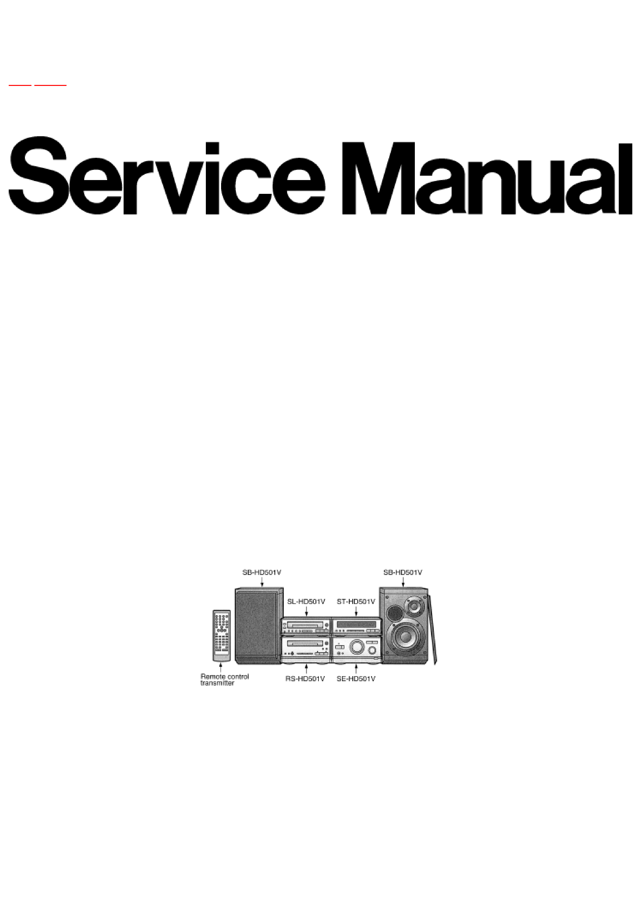
SE-HD501V
Colour
(N).......................Gold Type
Areas
GC........................Asia,Latin America,Middle Near East and Africa.
GK........................China.
System: SC-HD501V
Because of unique interconnecting cables, when a
compact requires service, send or bring in the entire
system.
Specification
·Amplifier Section (Low frequency side)
Power output
DIN 1kHz, THD 1%, both channels driven:
2x12W(6)
RMS 1 kHz, THD 10%, both channels driven:
2x15W(6)
Total harmonic distortion
Half power at 1 kHz:
0.09%(6)
Load impedanced:
6
S/N:
75dB
file:///E:/SEHD/OT/SE-HD501V/SVC/s0000000000.html (1 z 2) [2006-09-11 14:34:40]
file:///E:/SEHD/OT/SE-HD501V/SVC/s0000000000.html
·Amplifier Section (High frequency side)
Power output
DIN 10kHz, THD 1%, both channels driven:
2x5W(6)
RMS 10kHz, THD 10%, both channels driven:
2x8W(6)
Load impedanced:
6
S/N:
75dB
Headphones
Jack type:
3.5mm STEREO
Load impedanced:
16-32
·General
Power consumption:
78W
STANDBY condition
Normal:9W
Eco:0.8W
Power supply
[For (GK) area]:
220V,AC50Hz
[For (GC) area]:
220-240V,AC 50/60Hz
Dimensions (WxHxD):
196x104x270mm
Weight:
3.4kg
Notes:
1.Specifications are subject to change without notice.
2.Dimensions and Weight are approximate.
3.Total harmonic distortion is measured by the digital spectrum analyzer.
System/SC-HD501V:
Tuner:ST-HD501V, Compact Disc Player:SL-HD501V, Amplifier:SE-HD501V, Cassette Deck:RS-HD501V, Speakers:SB-HD501V (Made in MESA.)
© 1999 Matsushita Electric Industrial Co., Ltd.//All rights reserved. Unauthorized copying and distribution is a violation of law.
·@
TOP NEXT
file:///E:/SEHD/OT/SE-HD501V/SVC/s0000000000.html (2 z 2) [2006-09-11 14:34:40]

file:///E:/SEHD/OT/SE-HD501V/SVC/SEHD501V.html
Table Of Contents
COVER
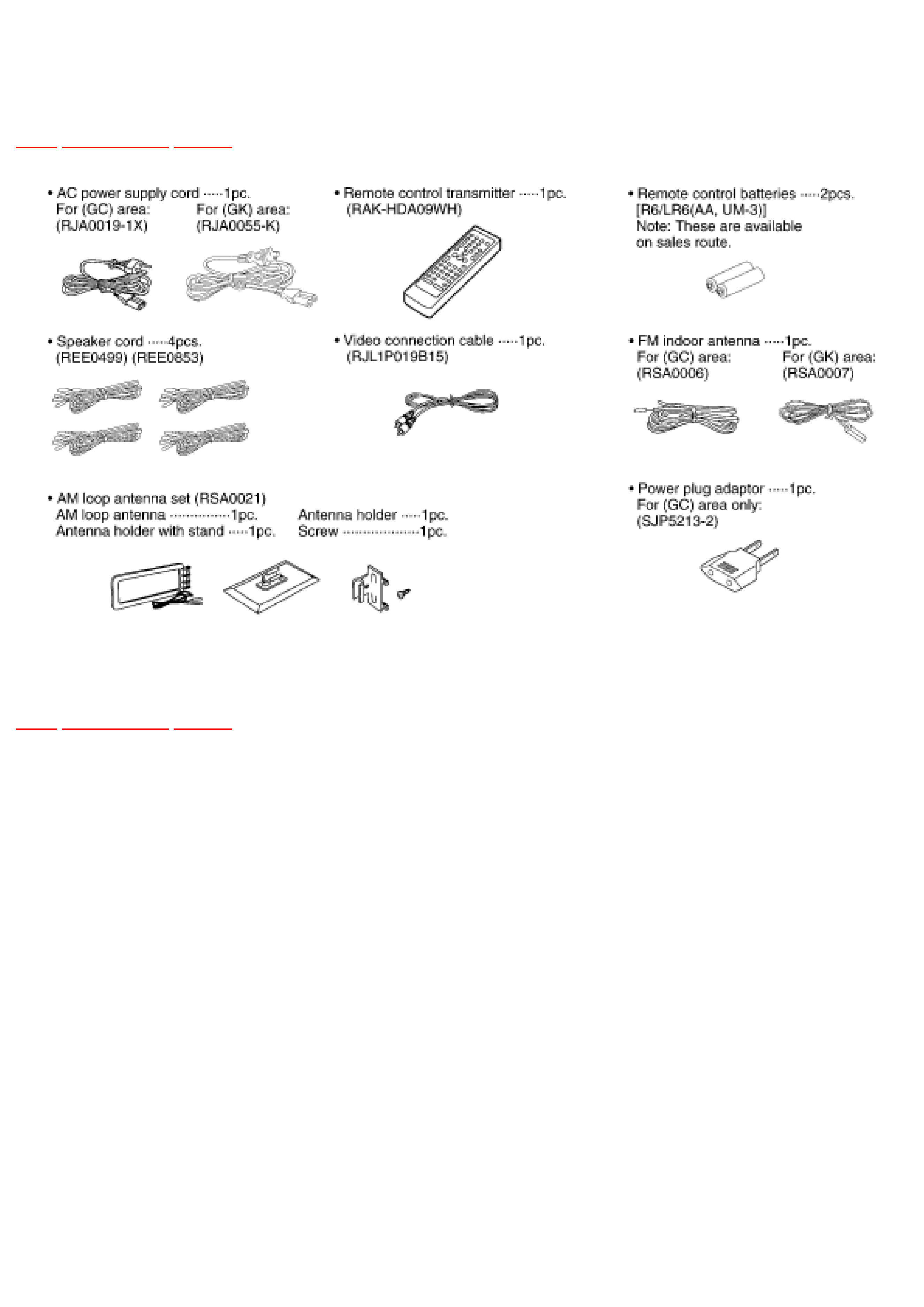
1 Accessories
2 Before Repair and Adjustment
3 Operating Instructions
4 Operation Checks and Component Replacement Procedures
5 Power Source ON/OFF and Signal Check
6 Schematic Diagram Notes
6.1 Type Illustration of ICs, Transistors and Diodes
6.2 Schematic Diagram Notes
7 Schematic Diagram
8 Printed Circuit Board Diagram
9 Block Diagram
10 Wiring Connection Diagram
11 Replacement Parts List
12 Cabinet Parts Location
13 Packaging
file:///E:/SEHD/OT/SE-HD501V/SVC/SEHD501V.html [2006-09-11 14:34:47]
PV
PV
file:///E:/SEHD/OT/SE-HD501V/SVC/s0100000000x.html
1 Accessories
TOP PREVIOUS NEXT
·@
TOP PREVIOUS NEXT
file:///E:/SEHD/OT/SE-HD501V/SVC/s0100000000x.html [2006-09-11 14:34:50]
file:///E:/SEHD/OT/SE-HD501V/SVC/s0200000000x.html
2 Before Repair and Adjustment
TOP PREVIOUS NEXT
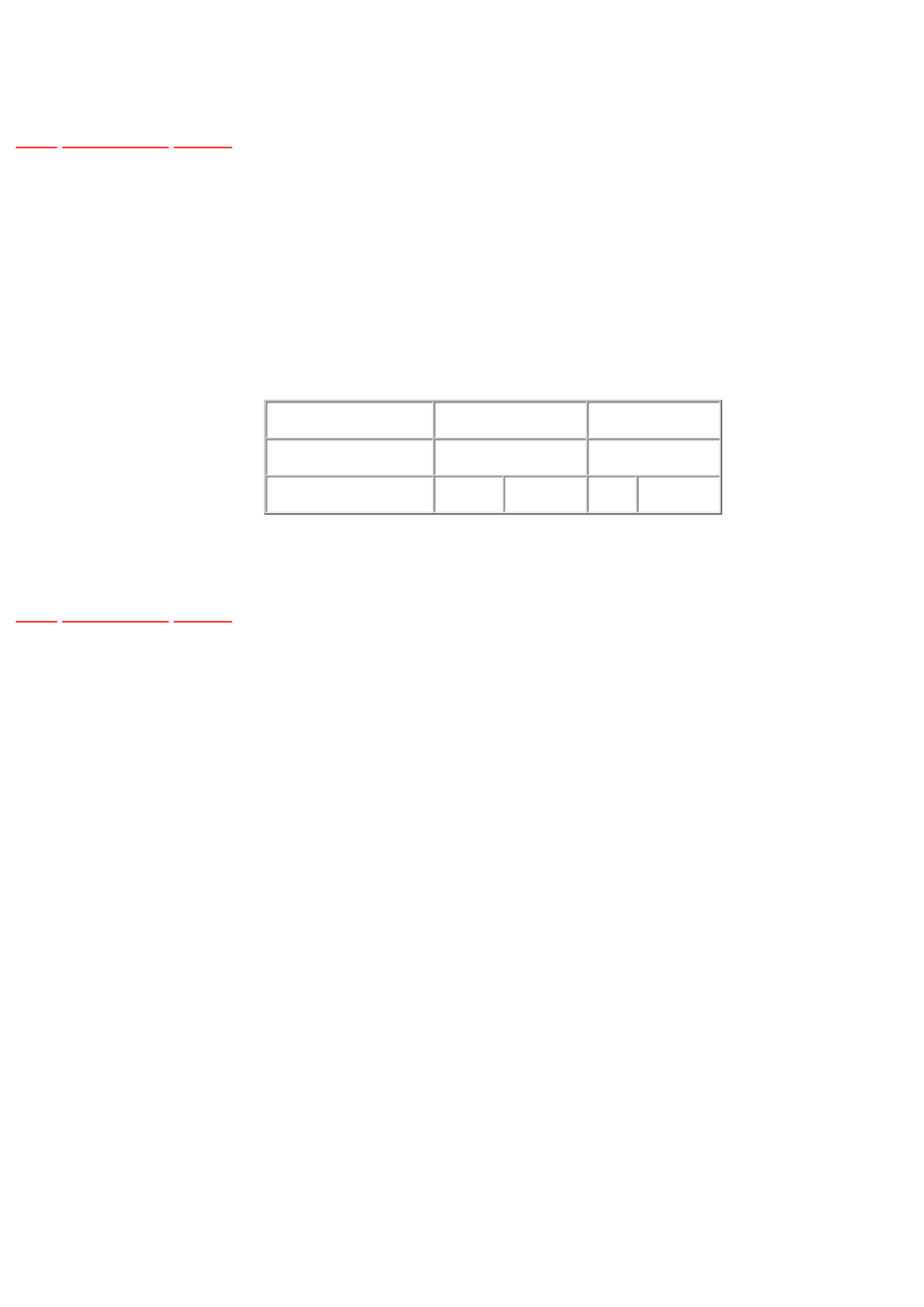
1. Turn off the power supply. Using a 10 , 10W resistor, connect both ends of power supply
capacitors (C102-105, 127) in order to discharge the voltage.
2. Before turning the power supply on, after completion of repair, slowly apply the primary
voltage by using a power supply voltage controller to make sure that the consumed current at
50/60 Hz in NO SIGNAL mode should be shown below withrespect to supply voltage 220 V-
240 V.
Area
(GC)
(GK)
Power supply voltage
AC 220-240V
AC 220V
Consumed current 50 Hz 50/60 Hz 50-150 mA 50 Hz 50-150 mA
·@
TOP PREVIOUS NEXT
file:///E:/SEHD/OT/SE-HD501V/SVC/s0200000000x.html [2006-09-11 14:34:58]