
file:///C|/Documents%20and%20Settings/bob/My%20Documents/manualdirectory.htm
This file was downloaded and provided FREE OF CHARGE
from the ManualDirectory community.
You can find many free to download Service Manuals & Schematics at
http://www.manualdirectory.co.uk
file:///C|/Documents%20and%20Settings/bob/My%20Documents/manualdirectory.htm01/04/2007 01:34:00
C
CR
R--H
H225
50
0
SERVICE MANUAL
CD Receiver
Effective : October, 2004
S-0130A
NOTES
PC boards shown are viewed from parts side.
The parts with no reference number or no parts number in the
exploded views are not supplied.
As regards the resistors and capacitors, refer to the circuit diagrams
contained in this manual.
£
Parts marked with this sign are safety critical components. They
must be replaced with identical components - refer to the appropriate
parts list and ensure exact replacement.
CONTENTS
1 SPECIFICATIONS
2
2 MICROCOMPUTER PIN FUNCTIONS
3
3 EXPLODED VIEWS AND PARTS LIST
11
4 PC BOARDS AND PARTS LIST
13
5 INCLUDED ACCESSORIES
17
For U.K.

1 SPECIFICATIONS
2
AMPLIFIER Section
Output Power .............................. 25 W/ch (6 ohms, 0.5 %,1 kHz)
Input Sensitivity ................................................ 300 mV/47k ohms
Frequency Response ...................... 20 Hz to 60,000 Hz (+1/-3 dB)
TUNER Section
FM Section
Tuning Range .............. 87.50 MHz to 108.00 MHz (50 kHz steps)
Signal-to-Noise Ratio .............................................. 65 dB (Mono)
60 dB (Stereo)
Presets ...................................................................................... 30
AM Section
Tuning Range .......................... 522 kHz to 1629 kHz (9 kHz steps)
Signal-to-Noise Ratio............................................................ 35 dB
Presets ...................................................................................... 30
DAB Section
Tuning Range ...................................... Band 3, 174 MHz-240 MHz
Input.................................................................. 50 ohms, nominal
Max Signal .................................................................. 3 dBm typ
Sensitivity .................................................................. 96 dBm typ
Adjacent Channel Rejection ............................................ 35 dB typ
Presets ...................................................................................... 10
Audio Output ........................................................ Stereo, 2.5 Vp-p
Digital Output .......................................... 24 bit/48 kHz resolution
CD PLAYER Section
Frequency Response .......................... 20 Hz to 20,000 Hz (±2 dB)
Signal-to-Noise Ratio .......................................... more than 85 dB
Wow and Flutter ...................................................... Unmeasurable
GENERAL
Power Requirements............................................ 230 V AC, 50 Hz
Power Consumption .............................................................. 75 W
(standby) .............................................................................. 2 W
Dimension (W x H x D) ................................ 215 x 110 x 359 mm
Weight ................................................................................ 4.4 kg
Standard Accessories
Remote Control Unit (RC-956) x 1
Batteries (AAA) x 2
AM Loop Antenna x 1
FM Lead-type Antenna x 1
DAB Antenna x 1
Owner's Manual x 1
Warranty Card x 1
· Design and specifications are subject to change without notice.
· Weight and dimensions are approximate.
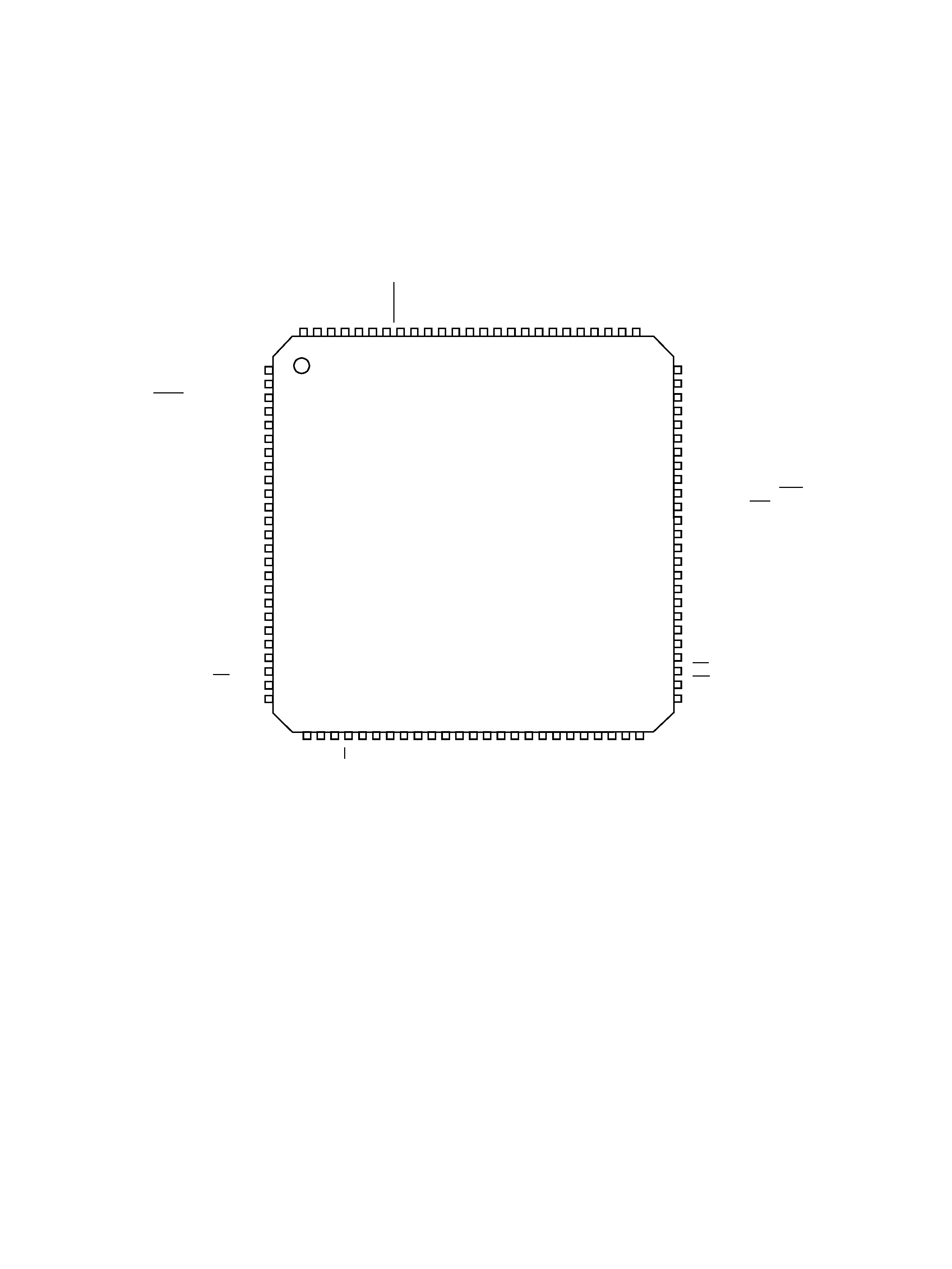
2 MICROCOMPUTER PIN FUNCTIONS
3
1
2
3
4
5
6
7
8
9
10
11
12
13
14
15
16
17
18
19
20
21
22
23
24
25
26 27 28 29 30 31 32 33 34 35 36 37 38 39 40 41 42 43 44 45 46 47 48 49 50
75
74
73
72
71
70
69
68
67
66
65
64
63
62
61
60
59
58
57
56
55
54
53
52
51
100 99 98 979695 949392 91 90898887 868584 83 82 81807978 7776
P8.4/AIN4
P8.3/AIN3
P8.2/AIN2
P8.1/AIN1/WKUP15
P8.0/AIN0/WKUP14
NC
P6.5/WKUP10/INTCLK
P6.4/NMI
P6.3/INT3/INT5
P6.2/INT2/INT4/DS2
P6.1/INT6/RW
P6.0/INT0/INT1/CLOCK2/8
P0.7/A7/D7
VDD
VSS
P0.6/A6/D6
P0.5/A5/D5
P0.3/A3/D3
P0.2/A2/D2
P0.1/A1/D1
P0.0/A0/D0
AS
DS
P0.4/A4/D4
P1.7/A15
A20/P9.6
WAIT/WKUP5/P5.0
WKUP6/WDOUT/P5.1
TXCLK/CLKOUT/P5.4
OCMPA1/P4.2
VDD
A21/P9.7
WDIN/SOUT/P5.3
DCD/WKUP8/P5.6
VSS
ICAPB1/OCMPB1/P4.3
SDA/P4.6
SIN/WKUP2/P5.2
RXCLK/WKUP7/P5.5
CLOCK2/P4.1
EXTCLK1/WKUP4/P4.4
ICAPB0/P3.1
ICAPA0/OCMPA0/P3.2
WKUP9/RTS/P5.7
ICAPA1/P4.0
EXTRG/STOUT/P4.5
WKUP1/SCL/P4.7
OCMPB0/P3.3
EXTCLK0/SS/P3.4
MISO/P3.5
P9
.5
/A1
9
P9
.4
/A1
8
P9
.2
/A1
6
HW
0S
W
1
P7
.7
/A
IN
1
5
/7
/W
K
U
P
1
3
P7
.4
/AI
N
1
2
/W
K
U
P
3
P9
.3
/A1
7
P9
.0
/R
D
I
R
ESET
P7
.6
/AI
N
1
4
/W
K
U
P
1
2
P7
.5
/AI
N
1
3
/W
K
U
P
1
1
P7
.1
/AI
N
9
P9
.1
/T
D
O
OS
C
IN
V
SS
P7
.3
/AI
N
1
1
P7
.0
/AI
N
8
/C
K_
A
F
P8
.7
/AI
N
7
OS
C
O
U
T
V
DD
P7
.2
/AI
N
1
0
AV
SS
AV
DD
P8
.6
/AI
N
6
P8
.5
/AI
N
5
MO
SI
/P3
.6
SC
K/
W
K
U
P
0
/P3
.7
RW
TO
U
T
A
0
/P
2
.2
V
SS
*V
TE
S
T
V
RE
G
TI
N
PB0
/P2
.1
TO
U
T
B
0
/P
2
.3
V
DD
V
RE
G
A
10/
P
1
.2
TI
N
PA0
/P2
.0
TI
N
PB1
/P2
.5
TO
U
T
B
1
/P
2
.7
A8
/P1
.0
A
11/
P
1
.3
A
12/
P
1
.4
TI
N
PA1
/P2
.4
TO
U
T
A
1
/P
2
.6
A9
/P1
.1
WK
U
P
6
NC
A
13/
P
1
.5
A
14/
P
1
.6
* VTEST must be kept low in standard operating mode.
ST92F124V1
ST92F124V1
PIN ASSIGNMENT
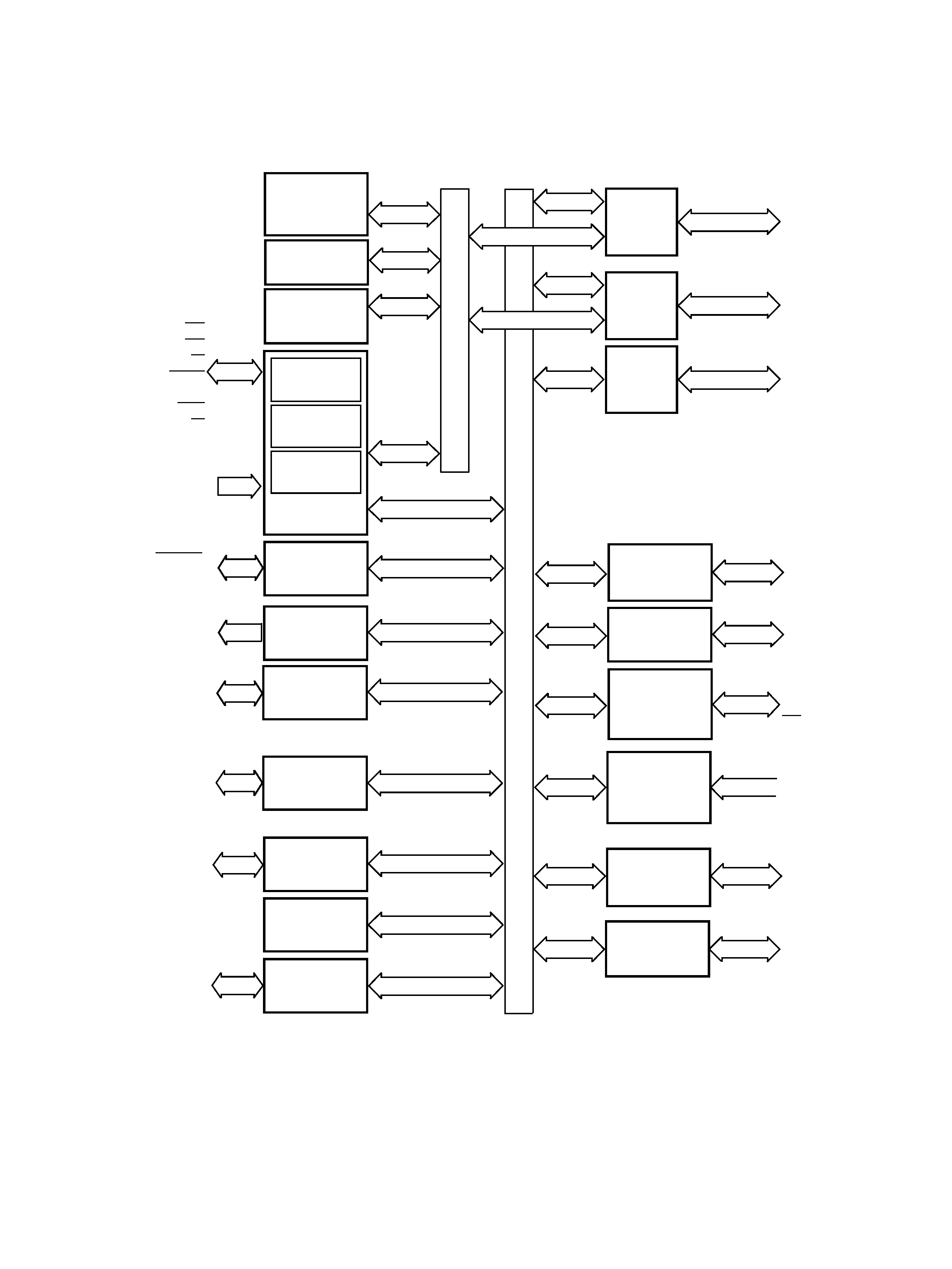
4
256 bytes
Register File
RAM
4 Kbytes
ST9 CORE
8/16 bits
CPU
Interrupt
Management
ME
MOR
Y
BU
S
RCCU
Ext. MEM.
ADDRESS
DATA
Port0
Ext. MEM.
ADDRESS
Ports
1,9
RE
GISTE
R
BU
S
WATCHDOG
AS
DS
RW
WAIT
NMI
DS2
RW
MISO
MOSI
SCK
SS
A[10:8]
A[21:11]
A[7:0]
D[7:0]
ST. TIMER
SPI
SDA
SCL
I2C BUS
FLASH
128 Kbytes
WDOUT
HW0SW1
STOUT
Fully
Prog.
I/Os
P0[7:0]
P1[7:3]
P1[2:0]
P2[7:0]
P3[7:4]
P3[3:1]
P4[7:4]
P4[3:0]
P5[7:0]
P6[5:2,0]
P6.1
P7[7:0]
P8[7:0]
P9[7:0]
MF TIMER 0
TINPA0
TOUTA0
TINPB0
TOUTB0
TINPA1
TOUTA1
TINPB1
TOUTB1
INT[6:0]
WKUP[15:0]
MF TIMER 1
E3 TM
1 Kbyte
OSCIN
OSCOUT
RESET
CLOCK2/8
INTCLK
CK_AF
ADC
AVDD
AVSS
AIN[15:8]
AIN[7:0]
EXTRG
VREG
VOLTAGE
REGULATOR
The alternate functions (
Italic characters) are mapped on Port 0, Port 1, Port2, Port3, Port4, Port5, Port6, Port7,
Port8 and Port9.
ICAPA0
OCMPA0
ICAPB0
OCMPB0
EXTCLK0
ICAPA1
OCMPA1
ICAPB1
OCMPB1
EXTCLK1
EF TIMER 0
EF TIMER 1
SCI M
TXCLK
RXCLK
SIN
DCD
SOUT
CLKOUT
RTS
SCI A
RDI
TDO
BLOCK DIAGRAM