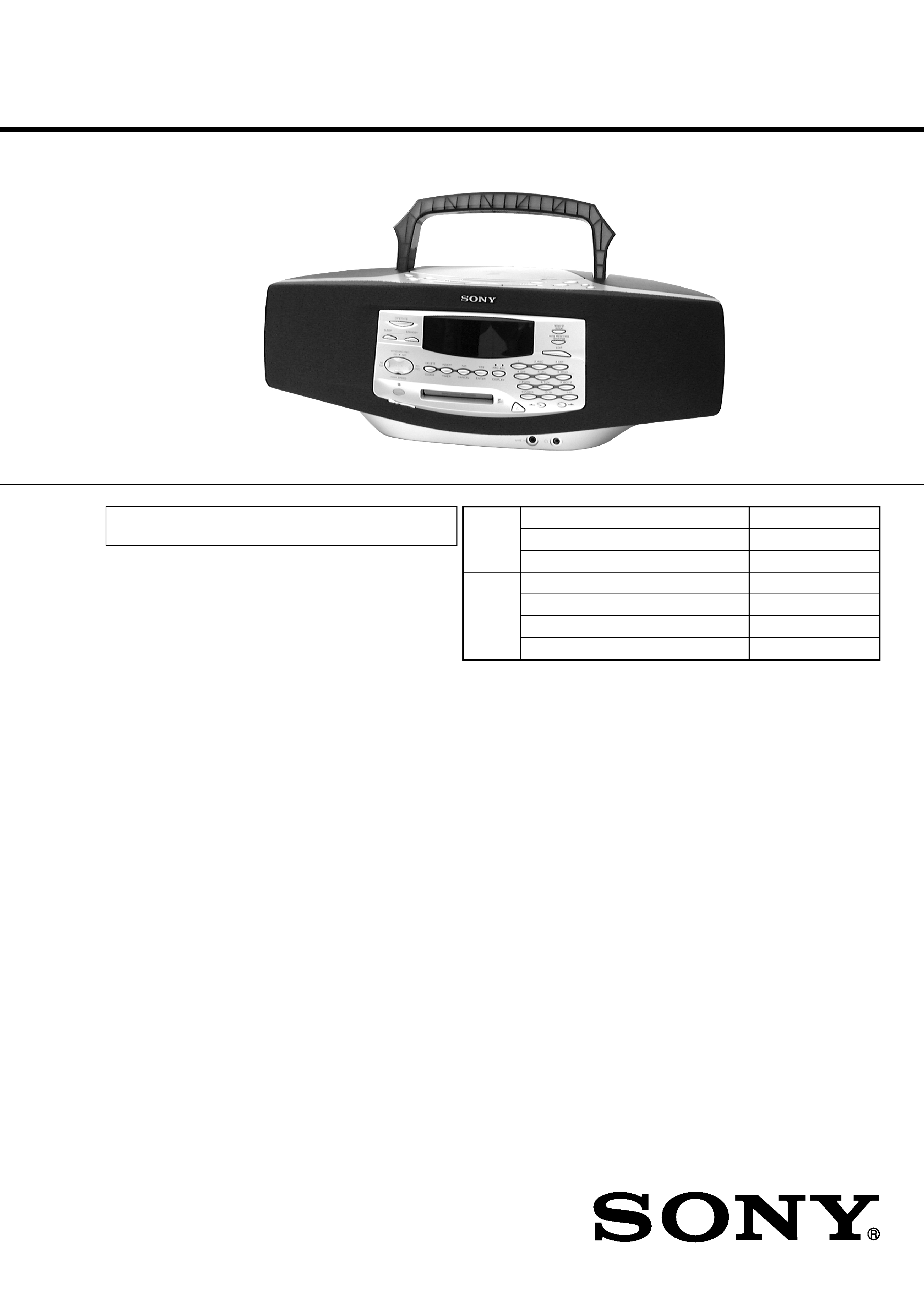
1
ZS-M35
SERVICE MANUAL
PERSONAL MINIDISC SYSTEM
AEP Model
UK Model
Tourist Model
CD
Model Name Using Similar Mechanism
ZS-M50
Section
CD Mechanism Type
KSM-213CDM
Optical Pick-up Name
KSS-213C
MD
Model Name Using Similar Mechanism
PMC-MD55
Section
MD Mechanism Type
MDM-5GA
Base Unit Name
MBU-5A
Optical Pick-up Name
KMS-260B
U.S. and foreign patents licensed from Dolby Laboratories
Licensing Corporation.
CD player section
System
Compact disc digital audio system
Laser diode properties
Material: GaAlAs
Wave length: 785 nm
Emission duration: Continuous
Laser output: Less than 44.6 µW
(This output is the value measured at a distance of
about 200 mm from the objective lens surface on
the optical pick-up block with 7 mm aperture.)
Spindle speed
200 r/min (rpm) to 500 r/min (rpm) (CLV)
Number of programme positions
2
Frequency response
20 - 20,000 Hz +1/2 dB
Wow and flutter
Below measurable limit
Radio section
Frequency range
FM: 87.5 - 108 MHz
MW: 531 - 1,602 kHz
LW: 153 - 279 kHz
IF
FM: 10.7 MHz
MW/LW: 450 kHz
Aerials
FM: Telescopic aerial
External aerial terminal
MW/LW: External aerial terminals
SPECIFICATIONS
MD player section
System
Minidisc digital audio system
Disc
MiniDisc
Laser diode properties
Material: GaAlAs
Wave length: 785 nm
Emission duration: Continuous
Laser output: Less than 44.6 µW
(This output is the value measured at a distance of
about 200 mm from the objective lens surface on
the optical pick-up block with 7 mm aperture.)
Recording/playback time
Stereo recording:
Maximum 80 minutes (with MDW-80)
Monaural recording:
Maximum 160 minutes (with MDW-80)
Revolutions
400 rpm to 900 rpm (CLV)
Error correction
Advanced Cross Interleave Reed Solomon Code
(ACIRC)
Sampling frequency
44.1 kHz
Continued on next page
Photo: black
Ver 1.3 2001.07
Sony Corporation
Personal Audio Company
Shinagawa Tec Service Manual Production Group
9-927-183-13
2001G0400-1
© 2001.7

2
Coding
Adaptive TRansform Acoustic Coding (ATRAC)
Modulation system
EFM (Eight-to-Fourteen Modulation)
Number of programme positions
2 stereo programme positions
Frequency response
20 - 20,000 Hz +1/2 dB
Signal-to-noise ratio
Over 80 dB (during playback)
Wow and flutter
Below measurable limit
General
Speaker
Full-range: 8 cm (3 in.) dia.,4 ohms, cone type (2)
Inputs
LINE IN (stereo minijack):Sensitivity 436 mV/
870 mV
Outputs
Headphones jack (stereo minijack) (1):
For 32 ohms impedance headphones
Maximum power output
5 W + 5 W
Power requirements
For personal minidisc system:
230 V AC, 50 Hz
For back-up memory:
4.5 V DC, 3 R6 (size AA) batteries
For remote control:
3 V DC, 2 R6 (size AA) batteries
Power consumption
24 W
Dimensions (incl.projecting parts)
approx. 498.5
× 173.5 × 227 mm (w/h/d)
(19 3/4
× 6 7/8 × 11 inches)
Mass
approx. 5.2 kg (11 lb. 7 oz)
Supplied accessories
Mains lead (1)
Remote control (RMT-CM35AD) (1)
MW/LW loop aerial (1)
Design and specifications are subject to change
without notice.

3
1. SERVICING NOTES
1-1. Notes on Handling the Optical Pick-up Block or Base Unit .. 4
1-2. Notes on Laser Diode Emission Check ............................... 4
1-3. Notes on Chip Component Replacement ............................ 4
1-4. Flexible Circuit Board Repairing ........................................ 4
1-5. Chuck Plate Jig on Repairing .............................................. 4
1-6. Demonstration ..................................................................... 4
1-7. Checking the Laser Diode and Focus Search Operation ..... 4
1-8. Jig for Checking BD Board Waveform ............................... 5
1-9. Checks Prior to Parts Replacement and Adjustments ......... 6
1-10. Change of Pulley ................................................................. 6
2. GENERAL
Playing a CD ....................................................................... 7
Recording a whole CD ........................................................ 7
Playing an MD ..................................................................... 8
Listening to the radio ........................................................... 8
3. DISASSEMBLY
3-1. Cabinet (Rear) Assy ............................................................ 9
3-2. Power Board ........................................................................ 9
3-3. Cabinet (Upper) Assy ........................................................ 10
3-4. MD Block Assy ................................................................. 10
3-5. Tuner Board ....................................................................... 11
3-6. Jack Board ......................................................................... 11
3-7. LED Board ........................................................................ 12
3-8. Key Board ......................................................................... 12
3-9. Top Board .......................................................................... 13
3-10. FL Board ........................................................................... 13
3-11. Main board ........................................................................ 14
3-12. CD Board .......................................................................... 14
3-13. CD Mechanism Block ....................................................... 15
3-14. DG Board .......................................................................... 15
3-15. Plate (Front), Shield .......................................................... 16
3-16. MD Mechanism Block-1 (MDM-5GA) ............................ 16
3-17. MD Mechanism Block-2 (Slider (Cam) Assy) ................. 17
3-18. MD Mechanism Block-3 (BD Board) ............................... 18
3-19. MD Mechanism Black-4 (SW Board) ............................... 18
4. TEST MODE
4-1. MD section ........................................................................ 19
5. ELECTRICAL ADJUSTMENTS
5-1. Tuner section ..................................................................... 24
5-2. MD section ........................................................................ 26
5-3. CD section ......................................................................... 33
TABLE OF CONTENTS
6. DIAGRAMS
6-1. IC Pin Function Descriptions ............................................ 35
6-2. Circuit Boards Location .................................................... 44
6-3. Block Diagram Tuner Section ....................................... 45
6-4. Block Diagram MD Section .......................................... 48
6-5. Block Diagram CD Section ........................................... 51
6-6. Block Diagram Audio Section ...................................... 53
6-7. Schematic Diagram CD Section (1/2) ........................... 55
6-8. Schematic Diagram CD Section (2/2) ........................... 57
6-9. Printed Wiring Boards CD Section ............................... 59
6-10. Printed Wiring Boards Tuner Section ........................... 61
6-11. Schematic Diagrams Tuner Section .............................. 63
6-12. Printed Wiring Boards BD Section ............................... 65
6-13. Schematic Diagram BD Section (1/2) ........................... 67
6-14. Schematic Diagrams BD Section (2/2) ......................... 69
6-15. Schematic Diagram DG Section ................................... 71
6-16. Schematic Diagram DG Section ................................... 73
6-17. Printed Wiring Board DG Section ................................. 75
6-18. Printed Wiring Board Main Section .............................. 77
6-19. Schematic Diagram Main Section (1/3) ........................ 79
6-20. Schematic Diagram Main Section (2/3) ........................ 81
6-21. Schematic Diagram Main Section (3/3) ........................ 83
6-22. Printed Wiring Boards Panel Section ............................ 85
6-23. Schematic Diagrams Panel Section ............................... 87
6-24. Printed Wiring Boards Switch Section .......................... 89
6-25. Schematic Diagrams Switch Section ............................ 91
6-26. Printed Wiring Boards Power Supply Section .............. 93
6-27. Schematic Diagrams Power Supply Section ................. 95
6-28. IC Block Diagrams ............................................................ 97
7. EXPLODED VIEWS
7-1. Cabinet (Rear) Section .................................................... 103
7-2. Cabinet (Front) Section ................................................... 104
7-3. Cabinet (Upper) Section .................................................. 105
7-4. MD Block Section ........................................................... 106
7-5. MD Mechanism Section (MDM-5GA) .......................... 107
7-6. MD Base unit Section (MBU-5A) ................................. 108
7-7. Optical Pick-up Section (KSM-213CDM) ...................... 109
8. ELECTRICAL PARTS LIST .................................... 110
4
SECTION 1
SERVICING NOTES
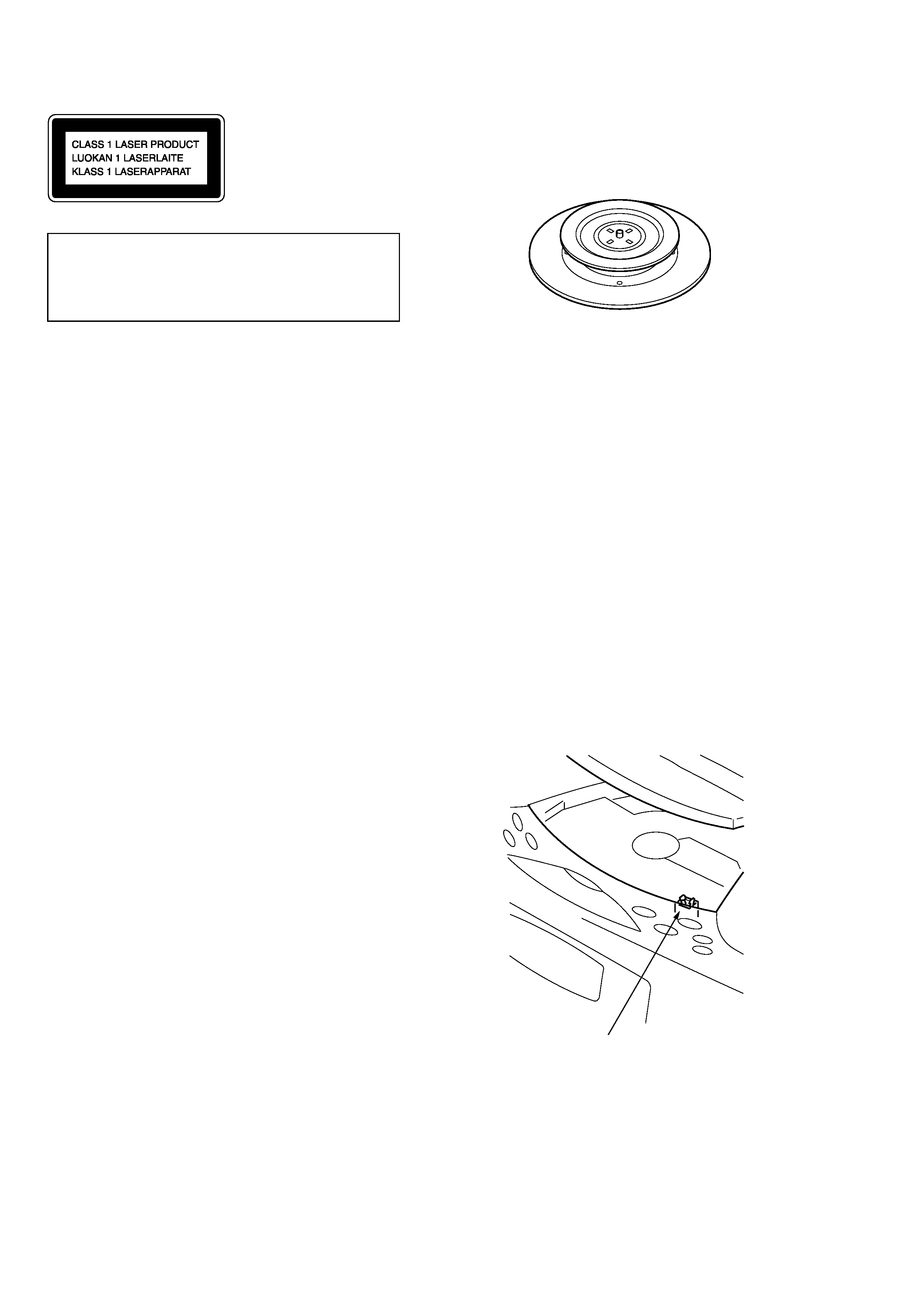
This Compact Disc player
is classified as a CLASS 1
LASER product.
The CLASS 1 LASER
PRODUCT label is located
on the bottom exterior.
SAFETY-RELATED COMPONENT WARNING!!
COMPONENTS IDENTIFIED BY MARK
0 OR DOTTED LINE
WITH MARK
0 ON THE SCHEMATIC DIAGRAMS AND IN
THE PARTS LIST ARE CRITICAL TO SAFE OPERATION.
REPLACE THESE COMPONENTS WITH SONY PARTS WHOSE
PART NUMBERS APPEAR AS SHOWN IN THIS MANUAL
OR IN SUPPLEMENTS PUBLISHED BY SONY.
1-1. NOTES ON HANDLING THE OPTICAL PICK-UP
BLOCK OR BASE UNIT
The laser diode in the optical pick-up block may suffer electro-
static break-down because of the potential difference generated
by the charged electrostatic load, etc. on clothing and the human
body.
During repair, pay attention to electrostatic break-down and also
use the procedure in the printed matter which is included in the
repair parts.
The flexible board is easily damaged and should be handled with
care.
1-2. NOTES ON LASER DIODE EMISSION CHECK
The laser beam on this model is concentrated so as to be focused
on the disc reflective surface by the objective lens in the optical
pick-up block. Therefore, when checking the laser diode emis-
sion, observe from more than 30 cm away from the objective lens.
1-3. NOTES ON CHIP COMPONENT REPLACEMENT
· Never reuse a disconnected chip component.
· Notice that the minus side of a tantalum capacitor may be dam-
aged by heat.
1-4. FLEXIBLE CIRCUIT BOARD REPAIRING
· Keep the temperature of the soldering iron around 270 °C dur-
ing repairing.
· Do not touch the soldering iron on the same conductor of the
circuit board (within 3 times).
· Be careful not to apply force on the conductor when soldering
or unsoldering.
1-5. CHUCK PLATE JIG ON REPAIRING
On repairing CD section, playing a disc without the CD lid, use
Chuck Plate Jig.
· Code number of Chuck Plate Jig: X-4918-255-1
1-6. DEMONSTRATION
This set enters the demonstration mode about 10 seconds after the
power cord is connected. The demonstration displays such as
"DEMONSTRATION MODE" and "CREATE YOUR ORIGINAL
MD" then appears.
When no operation is entered for one minute after the
[OPERATE]
button is turned on, the demonstration mode is also entered.
To release the demonstration mode, set the timer in this set or press
and hold down the
[NO/CANCEL] button for about 2 seconds.
1-7. CHECKING THE LASER DIODE AND FOCUS
SEARCH OPERATION
1. Turn on the POWER and open the CD cover.
2. As shown below, push S402 (CD DOOR) with a screwdriver or
other tool.
3. Press the CD button.
4. Check the objective lens to make sure that the laser diode is
emitting light. If not so, the auto power control circuit or optical
pickup would be damaged.
Verify that the objective lens moves vertically three times for
focus search.
S402
CAUTION
Use of controls or adjustments or performance of proce-
dures other than those specified herein may result in haz-
ardous radiation exposure.
5
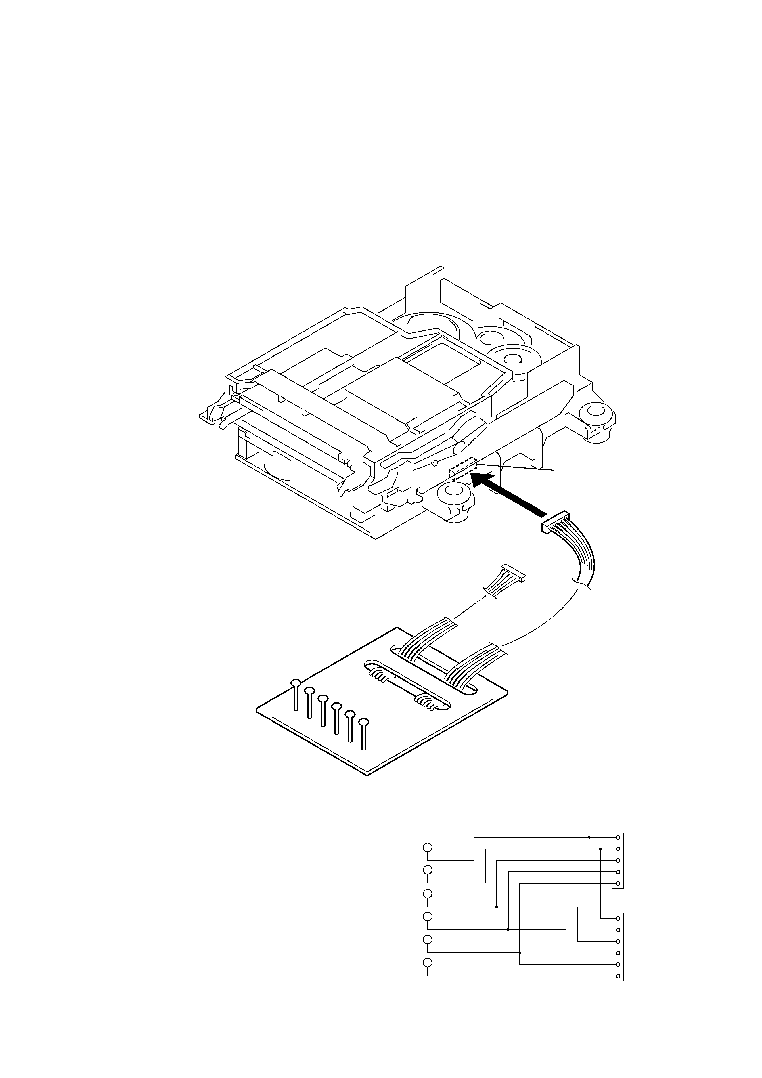
1-8. JIG FOR CHECKING BD BOARD WAVEFORM
The special jig (J-2501-149-A) is useful for checking the waveform of the BD board. The names of terminals and the checking items to
be performed are shown as follows.
GND : Ground
I+3V : For measuring IOP (Check the deterioration of the optical pick-up laser)
IOP : For measuring IOP (Check the deterioration of the optical pick-up laser)
TEO : TRK error signal (Traverse adjustment)
VC
: Reference level for checking the signal
RF
: RF signal (Check jitter)
CN110
RF
5P connector
6P connector
VC
TEO
IOP
I+3V
GND
Mechanism deck
RF
VC
TEO
for MDM-3
for MDM-5
IOP
I+3V
VC
RF
TEO
IOP
I+3V
GND
VC
RF
TEO
IOP
I+3V
GND
1
5
1
6