US Model
Canadian Model
AEP Model
UK Model
E Model
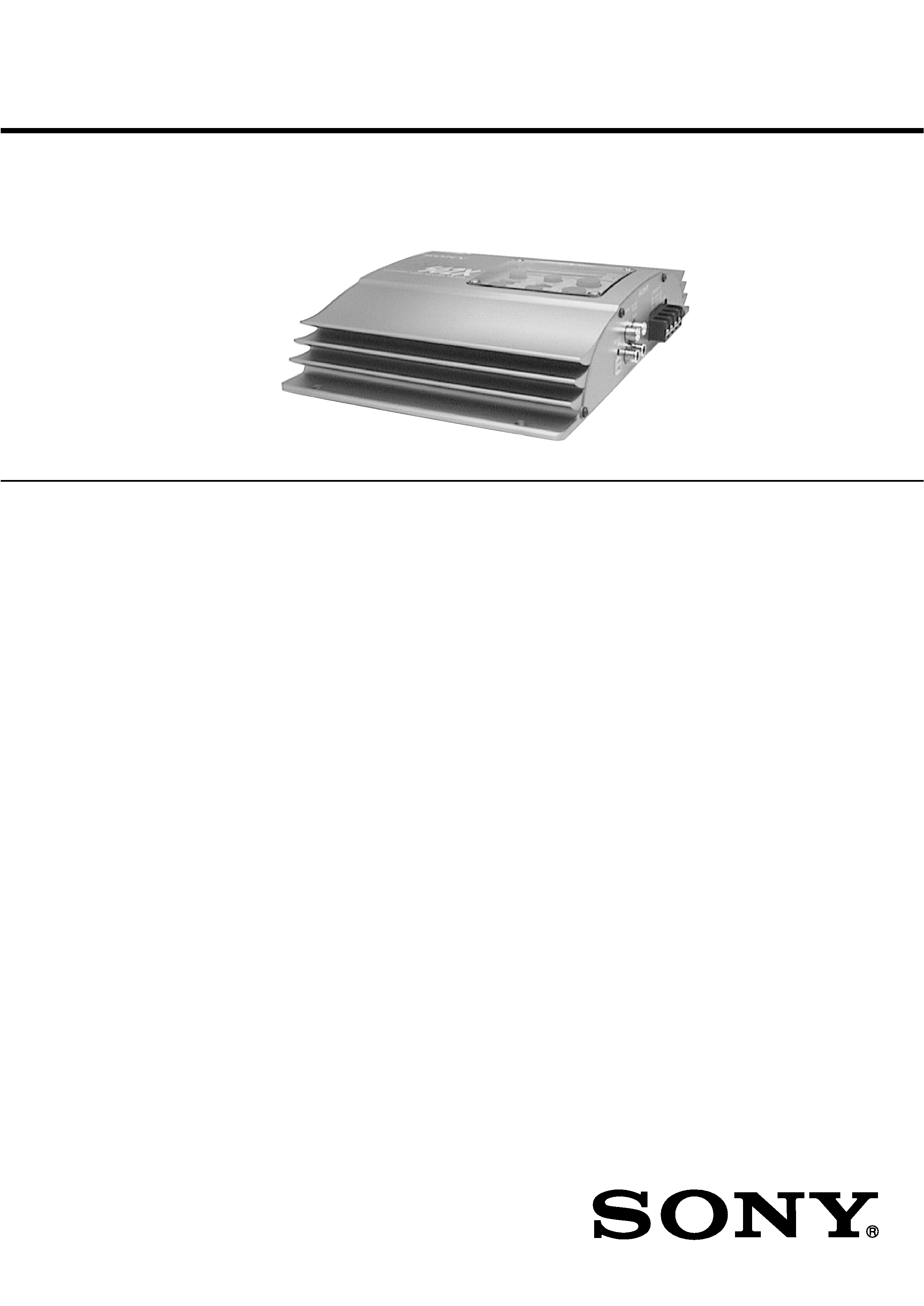
STEREO POWER AMPLIFIER
XM-502X
SERVICE MANUAL
Circuit system
OTL (output transformerless) circuit
Pulse power supply
Inputs
RCA pin jacks
High level input connector
Outputs
Speaker terminals
Through out pin jacks
Speaker impedance
2 - 8 ohms (stereo)
4 - 8 ohms (when used as a bridging
amplifier)
Maximum outputs
100 watts per channel (at 4 ohms)
260 watts (monaural) at 4 ohms
Rated outputs (supply voltage at 14.4 V)
50 watts per channel (20 Hz -
20 kHz, 0.04 % THD, at 4 ohms)
65 watts per channel (20 Hz -
20 kHz, 0.1 % THD, at 2 ohms)
130 watts (monaural) (20 Hz -
20 kHz, 0.1 % THD, at 4 ohms)
Frequency response
5 Hz - 100 kHz (
dB)
Harmonic distortion
0.005 % or less
(at 1 kHz, 4 ohms)
Input level adjustment range
0.2 - 4.0 V (RCA pin jacks)
0.4 - 8.0 V (High level input)
SPECIFICATIONS
High-pass filter
50 - 200 Hz, 12 dB/oct
Low-pass filter
50 - 200 Hz, 12 dB/oct
Low boost
0 - 10 dB (40 Hz)
Power requirements
12 V DC car battery
(negative ground)
Power supply voltage
10.5 - 16 V
Current drain
at rated output: 15 A
Remote input: 2 mA
Dimensions
Approx. 258
× 55 × 182 mm
(10 1/4
× 2 3/8 × 7 1/4 in.)
(l/h/p) not incl. projecting parts and
controls
Mass
Approx. 1.9 kg (4 lb. 3 oz.)
not incl. accessories
Supplied accessories
Mounting screws (4)
High level input cord (1)
Protect cover (1)
Design and specifications are subject to change without
notice.
+0
3
Ver 1.1 2001. 08
Sony Corporation
e Vehicle Company
Shinagawa Tec Service Manual Production Group
9-925-591-12
2001H0400-1
© 2001. 8

2
TABLE OF CONTENTS
1. GENERAL
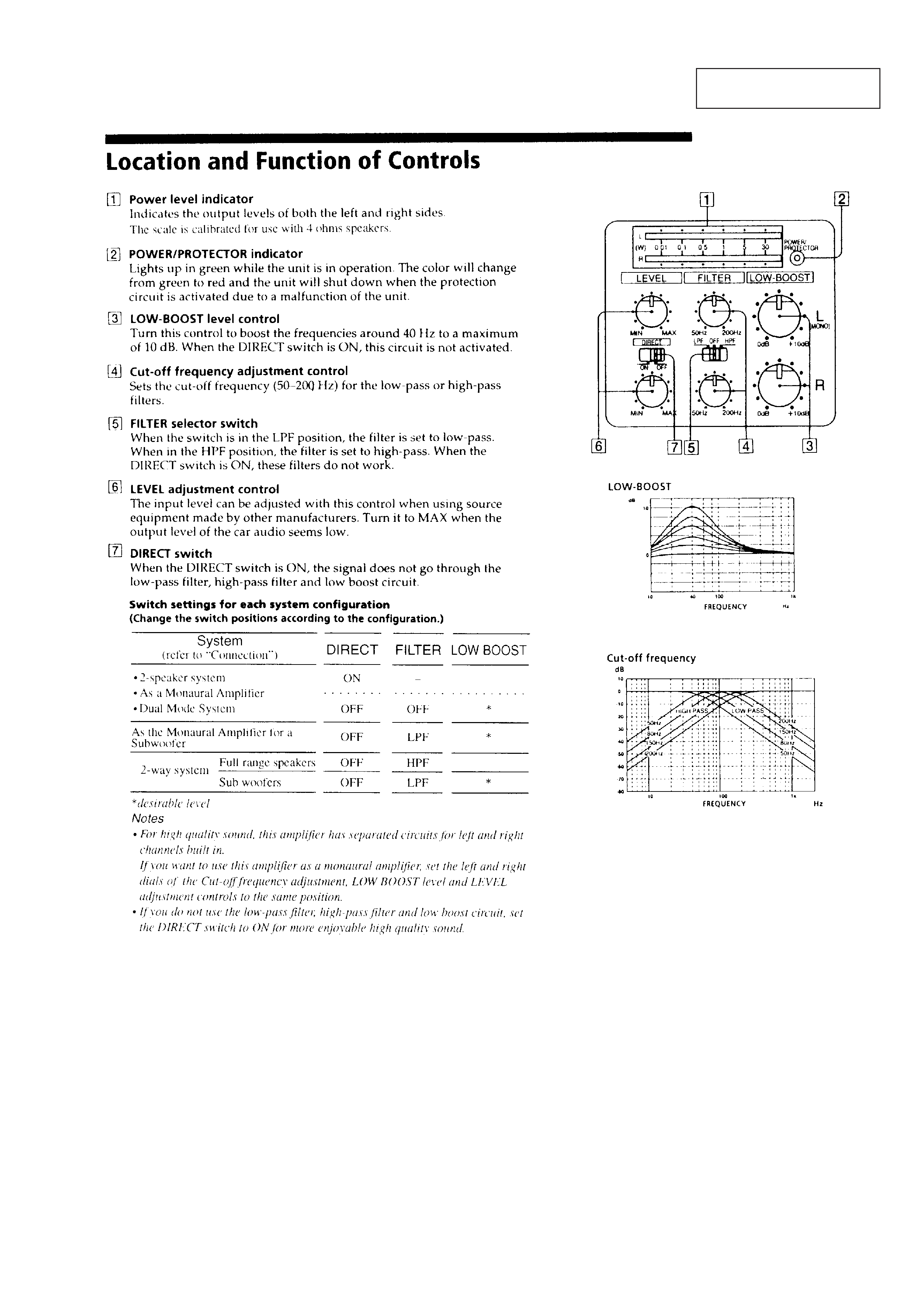
Location and Function of Controls ......................................... 3
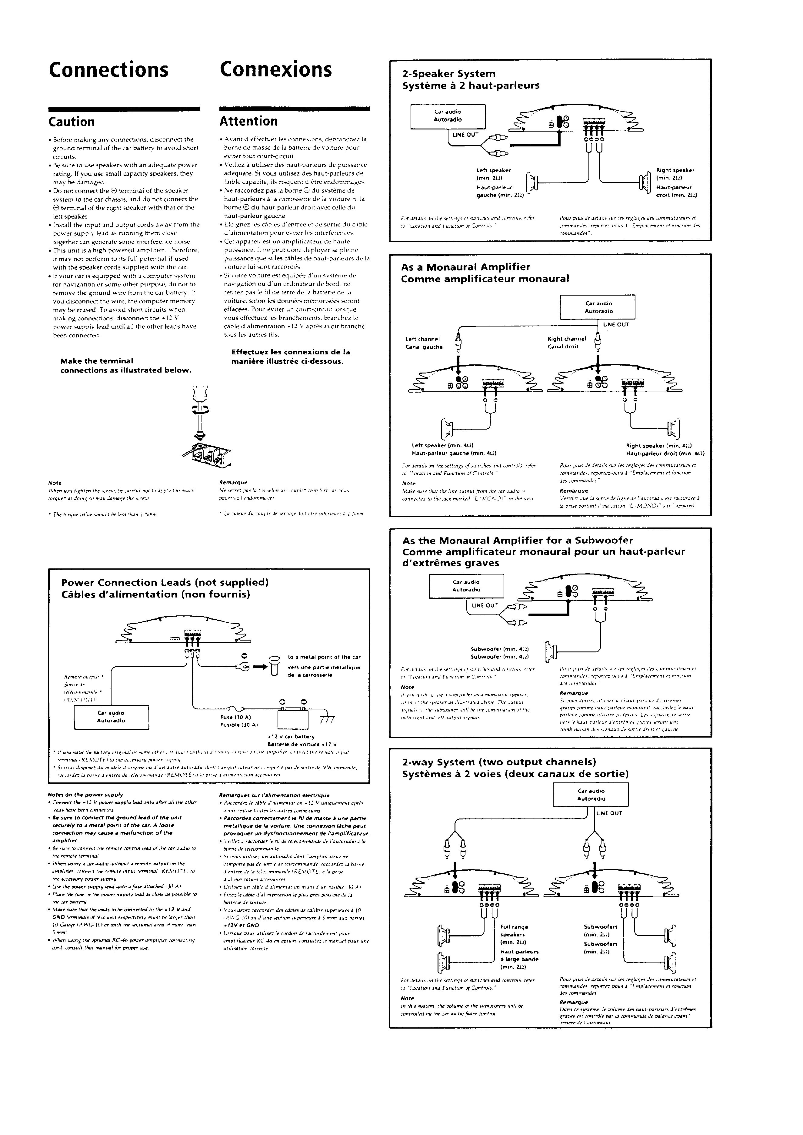
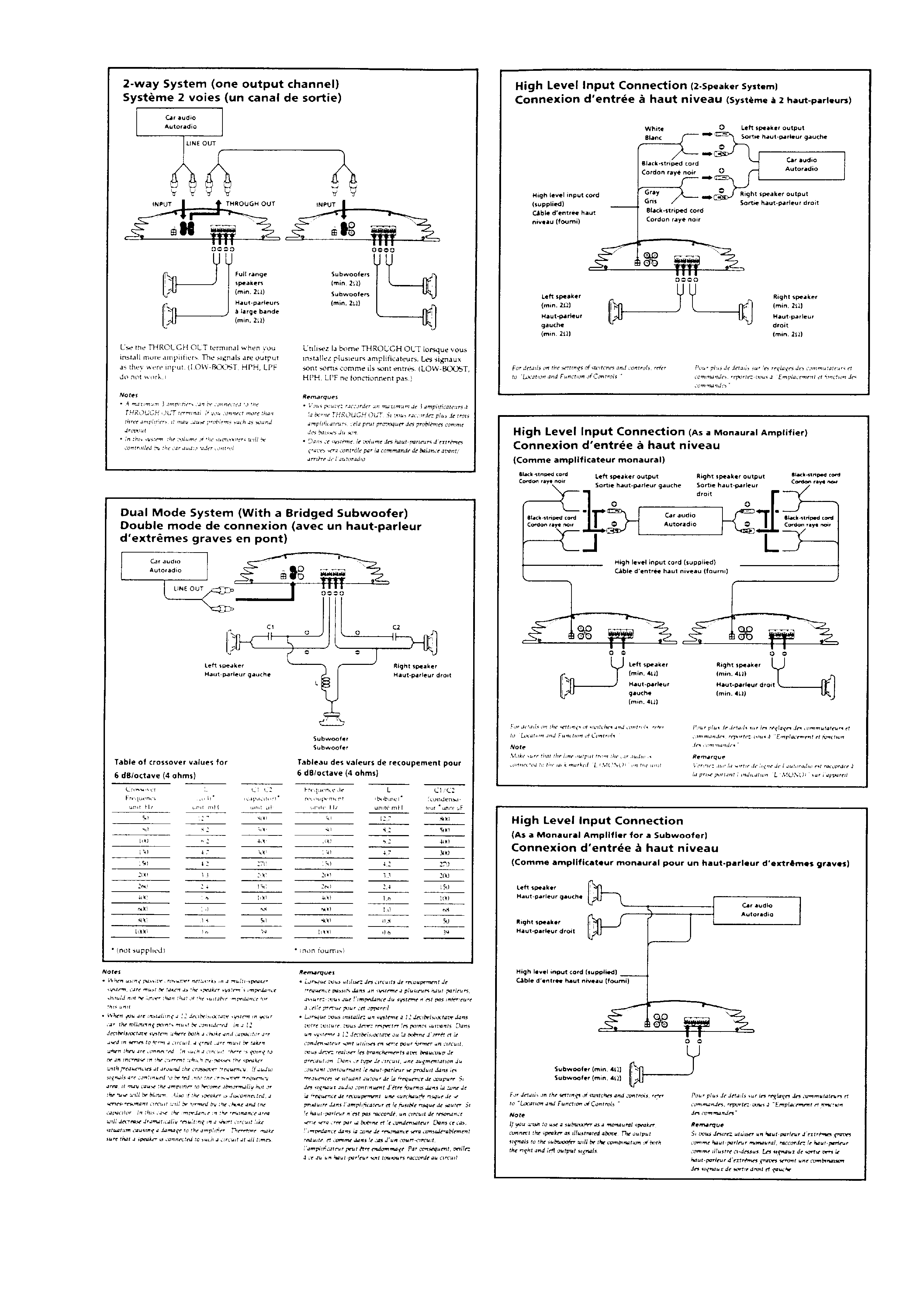
Connections ............................................................................ 4
2. DISASSEMBLY
2-1. Bottom Plate ....................................................................... 6
2-2. Panel (Front) ....................................................................... 6
2-3. Amplifier Board ................................................................. 7
2-4. Filter Board ........................................................................ 7
3. DIAGRAMS
3-1. Block Diagram ................................................................... 8
3-2. Printed Wiring Boards ...................................................... 10
3-3. Schematic Diagram .......................................................... 13
4. EXPLODED VIEWS
4-1. Amplifier Board Section .................................................. 17
4-2. Filter Board Section ......................................................... 18
5. ELECTRICAL PARTS LIST ................................... 19
Notes on Chip Component Replacement
· Never reuse a disconnected chip component.
· Notice that the minus side of a tantalum capacitor may be dam-
aged by heat.
3
SECTION 1
GENERAL
This section extracted from
instruction manual.
4
5