SERVICE MANUAL
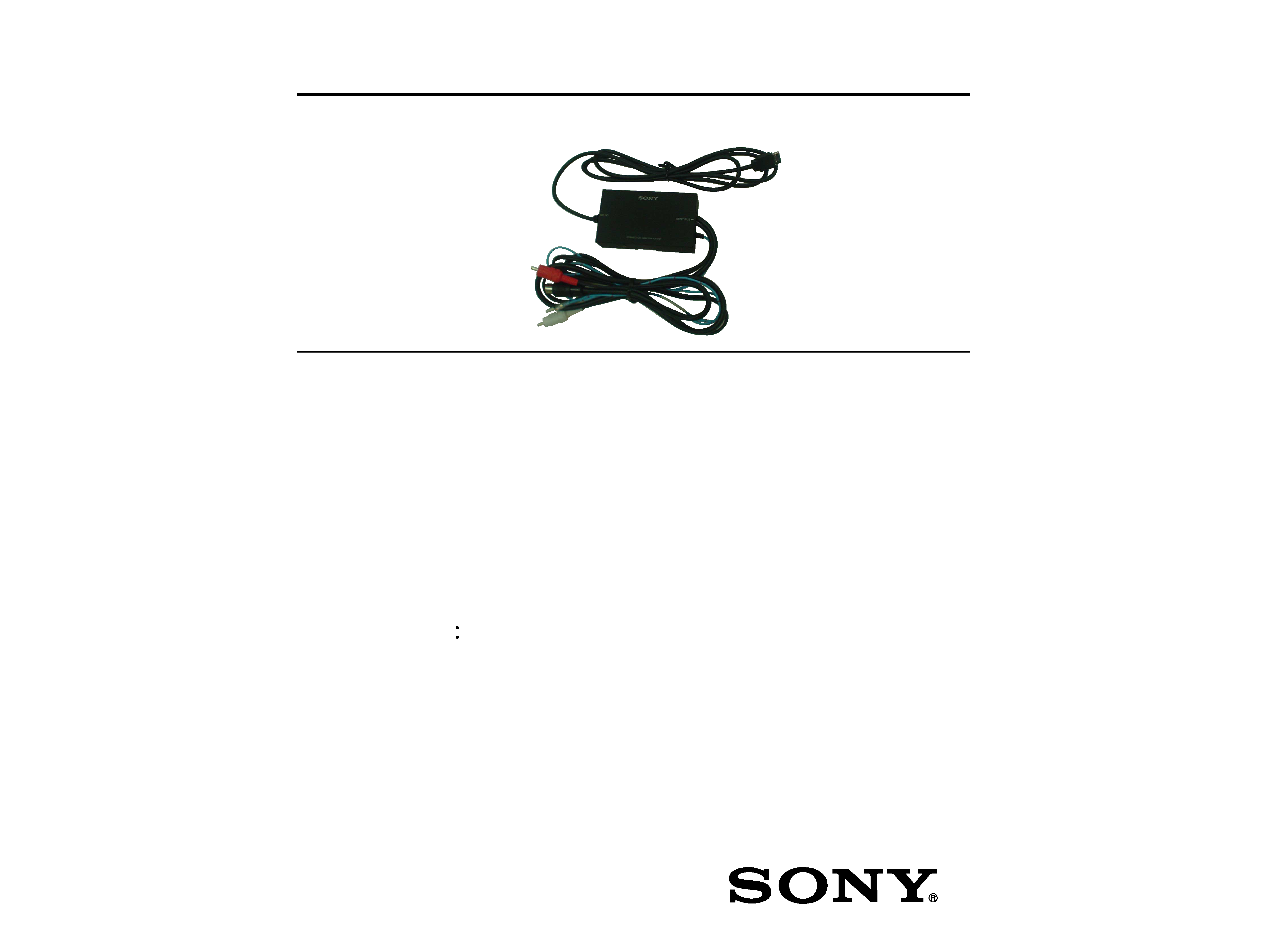
CONNECTION ADAPTER
US Model
SPECIFICATIONS
XA-CC1
Ver 1.0 2003.07
9-877-463-01
Sony Corporation
2003G05-1
e Vehicle Company
C
2003.07
Published by Sony Engineering Corporation
Power requirement
12 V DC negative ground
Dimensions
Approx. 97.2
55.7
23.7 mm
( 3 7/8
× 2 1/4 × 15/16 in.)
(w/h/d)
(not including connection cable)
Mass
Approx. 260 g (10 oz.)
(including connection cable)
Input
Car cradle I/O input (8pin)
Output
SONY-BUS control output (8pins)
SONY-BUS audio output (RCA-pin)
ATT control output
Design and specifications are subject to change without notice.
Features
The XA-CC1 is a connection adapter for connecting a car cradle to a Sony master unit having the CD/
MD changer control function.
Car Cradle Ready Sony car audio units are ;
Units with CD/MD Changer Control from 2003 forward
Following units
MEX-5DI, CDX-MP70, CDX-MP30, CDX-M730, CDX-M630, CDX-CA900X, CDX-CA720X,
CDX-CA700X, CDX-CA705M, XR-CA630X, XR-CA430X

2
XA-CC1
1.
GENERAL ................................................................... 3
2.
DIAGRAMS ................................................................. 4
2-1. Note for Printed Wiring Boards and
Schematic Diagram .........................................................
4
2-2. Schematic Diagram .........................................................
5
2-3. Printed Wiring Board
BUS Board (Component Side) .................................
6
2-4. Printed Wiring Board
BUS Board (Conductor Side) ...................................
7
2-5. IC Pin Function Description ...........................................
8
3.
EXPLODED VIEW ................................................... 9
4.
ELECTRICAL PARTS LIST ............................... 10
TABLE OF CONTENTS
Notes on chip component replacement
·Never reuse a disconnected chip component.
· Notice that the minus side of a tantalum capacitor may be dam-
aged by heat.
UNLEADED SOLDER
Boards requiring use of unleaded solder are printed with the lead-
free mark (LF) indicating the solder contains no lead.
(Caution: Some printed circuit boards may not come printed with
the lead free mark due to their particular size)
: LEAD FREE MARK
Unleaded solder has the following characteristics.
· Unleaded solder melts at a temperature about 40 °C higher than
ordinary solder.
Ordinary soldering irons can be used but the iron tip has to be
applied to the solder joint for a slightly longer time.
Soldering irons using a temperature regulator should be set to
about 350 °C.
Caution: The printed pattern (copper foil) may peel away if the
heated tip is applied for too long, so be careful!
· Strong viscosity
Unleaded solder is more viscou-s (sticky, less prone to flow)
than ordinary solder so use caution not to let solder bridges oc-
cur such as on IC pins, etc.
· Usable with ordinary solder
It is best to use only unleaded solder but unleaded solder may
also be added to ordinary solder.
3
XA-CC1
SECTION 1
GENERAL
This section is extracted from
instruction manual.
Installation
Before installation
Choose the installation location carefully so that the unit does not interfere with normal driving operations.
Avoid installing the unit where it would be subject to :
high temperatures, such as from direct sunlight or hot air from the heater.
draft, rain or moisture.
dust or dirt.
magnetic fields.
Install the unit at a to location that does not obstruct the operation of passenger-side airbag.
Installation location
Install the unit inside the car panel or glove box is recommended.
Please consult qualified technician or service personnel if you cannot attach the connection adapter to the car securely.
If you have any questions or problems concerning your unit that are not covered in this manual, please consult your nearest Sony dealer.
Before making any connection, disconnect the ground terminal of the car battery to avoid short
circuits.
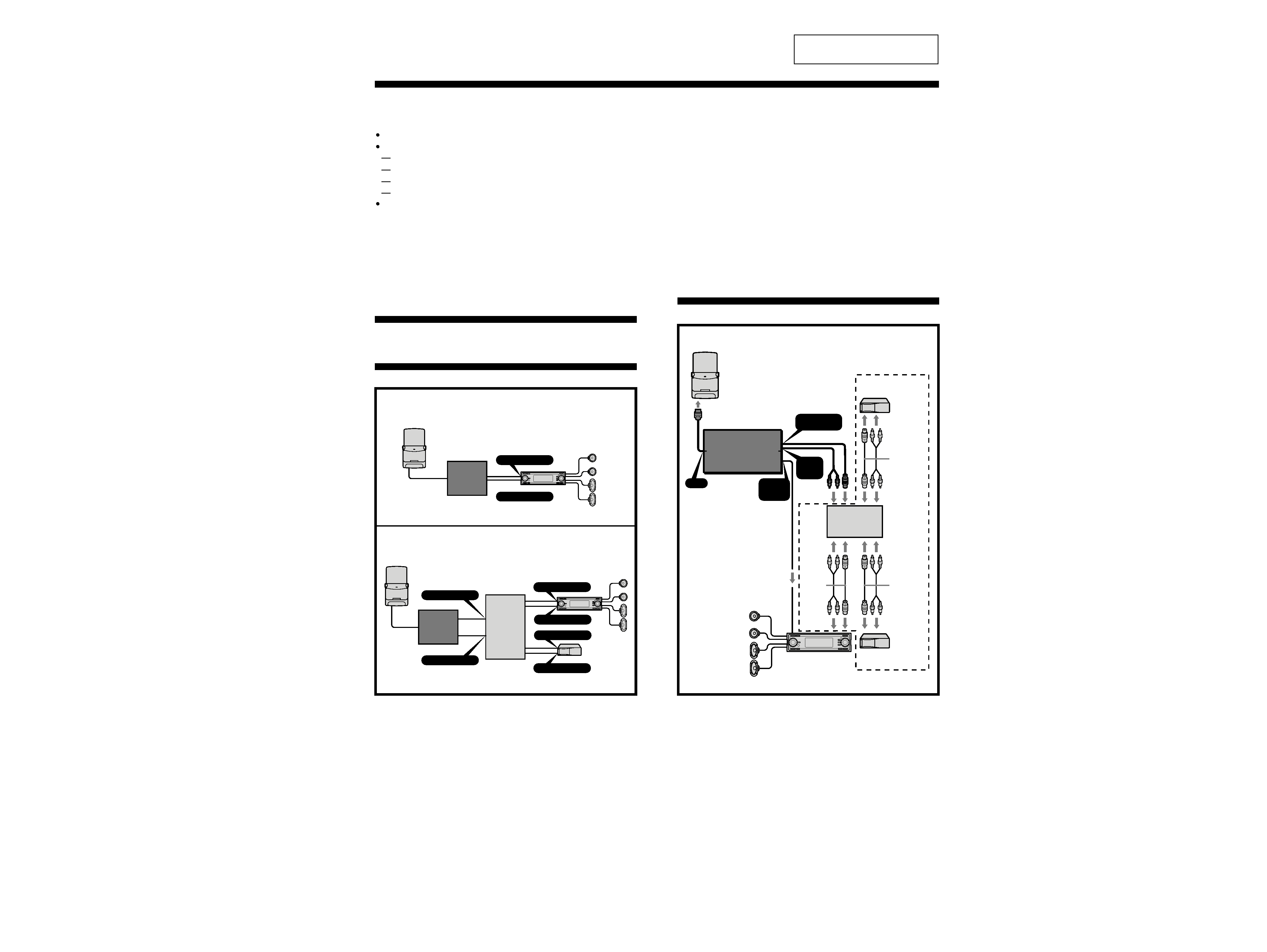
Connections
Precautions
Connection diagram
Connection example
A
I / O
SONY BUS
BUS AUDIO IN
BUS CONTROL IN
BUS CONTROL IN
Connection
Adapter
XA-CC1
Source
selector
XA-C30
(optional)
Connection
Adapter
XA-CC1
Light blue
ATT
Car cradle
Supplied with
the CD/MD
changer
BUS AUDIO IN
Source selector
XA-C30
(optional)
Sony BUS compatible
CD/MD changer
(optional)
Sony BUS compatible
car audio
Supplied with
the CD/MD
changer
Sony BUS compatible
CD/MD changer
(optional)
BUS CONTROL IN
BUS AUDIO IN
BUS CONTROL OUT
Rear speaker
Front speaker
B
Supplied
with the
XA-C30
1.6m
1m
1m
1m
Car cradle
Car cradle
BUS AUDIO OUT
BUS
CONTROL OUT
BUS
AUDIO
OUT
ATT
or
ATT OUT
I/O
ATT
4
XA-CC1
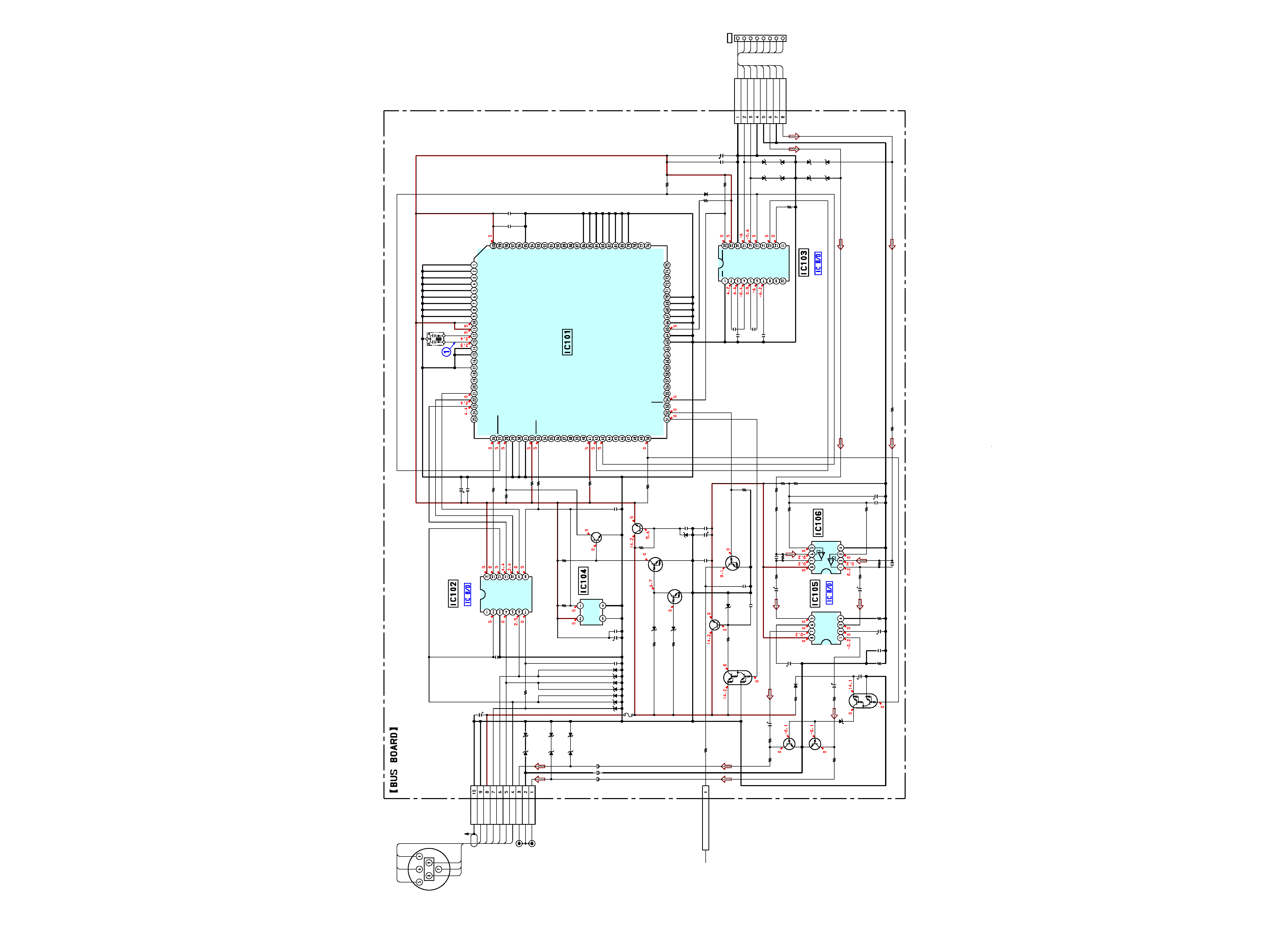
2-1.
NOTE FOR PRINTED WIRING BOARDS AND SCHEMATIC DIAGRAM
SECTION 2
DIAGRAMS
Note on Schematic Diagram:
· All capacitors are in µF unless otherwise noted. pF: µµF
50 WV or less are not indicated except for electrolytics
and tantalums.
· All resistors are in and 1/4 W or less unless otherwise
specified.
·
f
: internal component.
· A : B+ Line.
·Power Voltage supplies dc 14.4V to CN102 from control
unit (Sony BUS compatible car audio).
no mark : MP3 PLAY
·Voltages are taken with a VOM (Input impedance 10 M).
Voltage variations may be noted due to normal produc-
tion tolerances.
·Waveforms are taken with a oscilloscope.
Voltage variations may be noted due to normal produc-
tion tolerances.
· Circled numbers refer to waveforms.
· Signal path.
F
: AUDIO
Note on Printed Wiring Boards:
·
f
: internal component.
·
: Pattern from the side which enables seeing.
(The other layers' patterns are not indicated.)
Caution:
Pattern face side:
Parts on the pattern face side seen from
(Conductor Side)
the pattern face are indicated.
Parts face side:
Parts on the parts face side seen from
(Component Side)
the parts face are indicated.
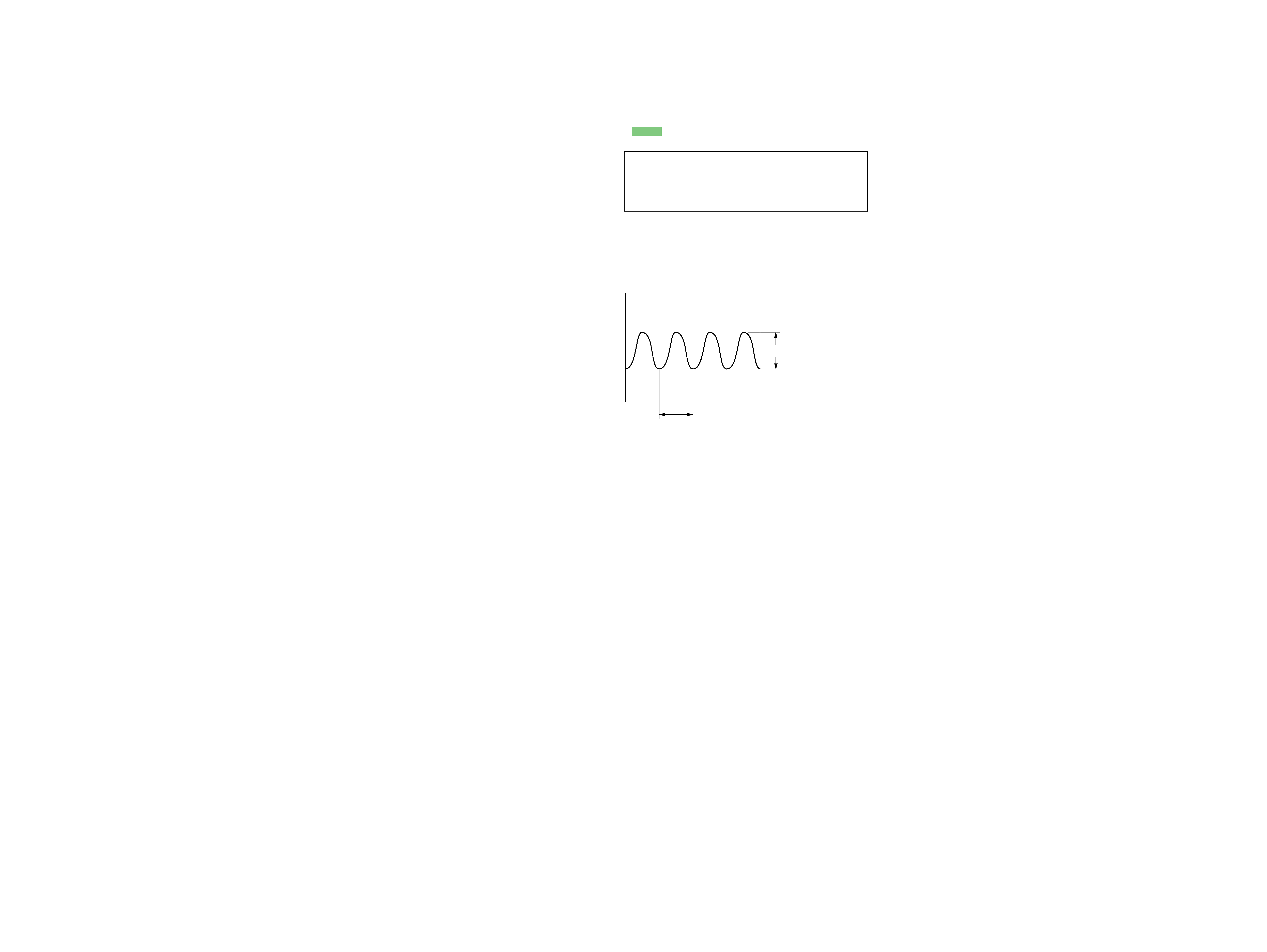
·Waveform
1
IC101 qs OSC2
4.9 Vp-p
54.4 ns
XA-CC1
5
5
2-2.
SCHEMATIC DIAGRAM · See page 4 for Waveform.
· See page 8 for IC Block Diagrams.
R110
C109
R139
D108
C133
C120
R142
D123
D122
D124
D125
D129
D130
D115
D113
R104
C137
C135
C136
C134
C132
C131
X101
R141
R106
R140
C110
C124
R143
IC103
IC102
R111
R109
R108
Q102
R107
C126
D107
C125
Q101
R101
C123
C122
D103
D106
D102
D105
D101
D121
D120
D126
D116
C142
R134
R133
R131
R129
R132
R125
R130
R121
Q103
Q104
R146
C130
C121
R147
C138
C139
R127
R123
C116
R128
R124
C115
IC106
R115
C128
D111
C129
C111
Q108
C112
R122
R102
C106
R118
R117
R119
C107
C103
R138
D114
C141
R116
Q112
Q113
D1117
D127
D128
D118
FB102
FB101
FB103
R137
C127
D112
Q107
D109
D110
CN103
IC101
IC104
Q105
IC105
Q106
C108
PS101
C102
CN102
C140
R105
R112
CN101
100k
100
10V
100k
MA728
0.1
10
16V
100k
MA8180-M
MA8180-M
MA8180-M
MA8180-M
MA8180-M
MA8180-M
MA8180-M
MA8180-M
0
0.1
0.1
0.1
0.1
0.1
0.1
18.432MHz
0
1k
0
10
16V
0.1
0
SP3222ECY
BA8272AFV-E2
100k
1k
1k
2SC2412K
47k
0.1
MA8056-M
0.1
2SD1664
47k
0.001
0.0047
MA728
MA8180-M
MA728
MA8180-M
MA728
MA8180-M
MA8180-M
MA8180-M
MA8180-M
0.1
10k
10k
10k
10k
10k
1.8k
10k
1.8k
DTC144EUA
DTC114EUA
2.7k
0.1
10
16V
100k
0.001
68p
22k
100
10
16V
22k
100
10
16V
NJM4580E
10k
0.1
MA8091-M
0.1
100
10V
DTC124EUA
0.1
470
0
10
16V
100
0
100
10
16V
10
16V
47
MA111
47
16V
0
DTC314TK
DTC314TK
MA8180-M MA8180-M
MA8180-M
MA8180-M
100k
0.1
MA8039
2SD1664
MA8068-M
MA8180-M
1P
MN101CP49KSD
XC61CN4002NR
XN1A312
BA3121F
XN1A312
33
10V
5A 24V
1000
16V
10P
68p
10k
10k
8P
BUS_GND
BUS_GND
RESET
DATA
CLK
BATT
BUS_ON
Rch
Lch
SGND
ATT
B.DATA
GND
B.CLK
VREF
RST.I
BUONO
BUONI
VCC
B.ON
L.OFF
CLK.O
D.O
D.I
RST
VIN
VSS
NC
VOUT
BUS_GND
TX
RX
Lch
SGND
Rch
SGND
BUS-GND
R2OUT
C1+
V+
C1-
C2+
V-
R2IN
T2OUT
C2-
EN
VCC
GND
T1OUT
R1IN
R1OUT
T1IN
T2IN
NC
NC
SHDN
V
R
E
F-
V
R
EF+
V
D
D
O
S
C
2
O
S
C
1
V
S
S
M
M
O
D
B
U
S
_
S
O
B
U
S
_
S
I
B
U
S
_
C
K
I
BUS_ON
DIN
RESET
DOUT
LINK_OFF
ATT
P
W
_O
N
A
C
C
_O
U
T
DAVSS
DAVDD
(VDD2)
(VPP)
SH
D
N
WAKE_UP
T
EL
_A
T
T
FLA
SH
_R
X
F
LA
S
H
_
TX
FL
AS
H
_W
BU_IN
IN
2
V
M
2
O
U
T2
V
C
C
O
U
T
1
IN
1
V
M
1
G
N
D
BUS CONTROLLER
RS-232C DRIVER
CLIE_TX
CLIE_RX
SONY BUS INTERFACE
RESET SIGNAL
GENERATOR
VOLTAGE
DETECT
Q103,104
BATTERY CHECK
LEVEL SHIFT
REGULATOR
-1
-2
REGULATOR
CONTROL
LINE AMP
GND
VCC
SPEAKER AMP
-1
-2
CONTROL
MUTING
MUTING
MUTING
I/O
(L)
(R)
(BUS AUDIO OUT)
(BUS CONTROL OUT)
ATT
REGULATOR
+5V