1
CD player section
Signal-to-noise ratio
92 dB
Frequency response
10 20,000 Hz
Wow and flutter
Below measurable limit
Laser Diode Properties
Material
GaAlAs
Wavelength
780 nm
Emission Duration
Continuous
Laser output power
Less than 44.6 µW*
* This output is the value measured at a distance
of 200 mm from the objective lens surface on
the Optical Pick-up Block.
Cassette player section
Tape track
4-track 2-channel stereo
Wow and flutter
0.08 % (WRMS)
Frequency response
30 18,000 Hz
Signal-to-noise ratio
Cassette type
Dolby B NR
Dolby NR off
TYPE II, IV
67 dB
58 dB
TYPE I
64 dB
55 dB
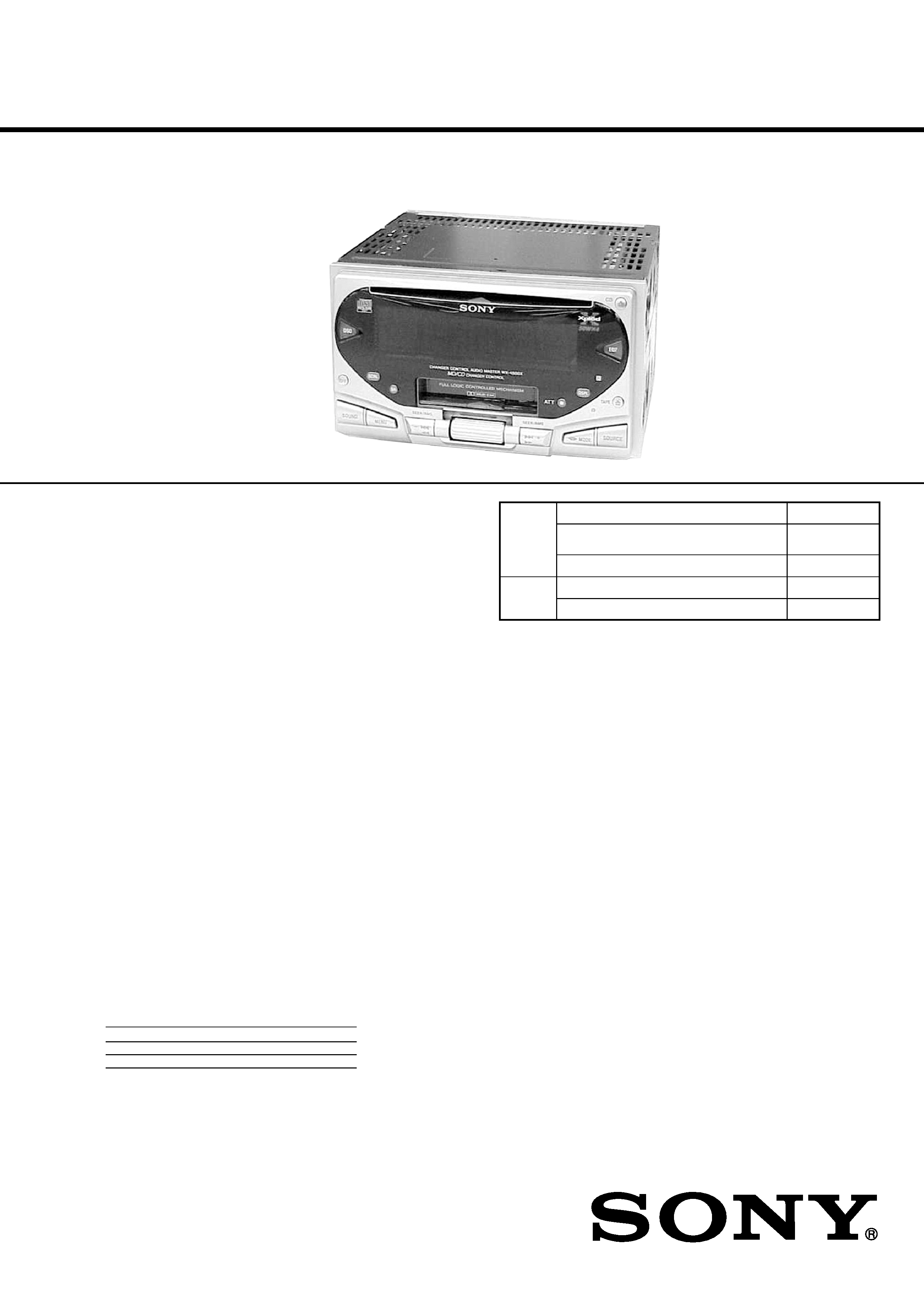
SERVICE MANUAL
US Model
WX-4500X
CHANGER CONTROL AUDIO MASTER
SPECIFICATIONS
Continued on next page
Dolby noise reduction manufactured under license from Dolby Labo-
ratories Licensing Corporation.
"DOLBY" and the double-D symbol ; are trademarks of Dolby
Laboratories Licensing Corporation.
AUDIO POWER SPECIFICATIONS
POWER OUTPUT AND TOTAL HARMONIC DISTORTION
23 watts per channel minimum continuous average power into
4 ohms, 4 channels driven from 20 Hz to 20 kHz with no more
than 5% total harmonic distortion.
Tuner section
FM
Tuning range
FM tuning interval:
50 kHz/200 kHz switchable
87.5 108.0 MHz
(at 50 kHz step)
87.5 107.9 MHz
(at 200 kHz step)
Antenna terminal
External antenna connector
Intermediate frequency 10.7 MHz/450 kHz
Usable sensitivity
8 dBf
Selectivity
75 dB at 400 kHz
Signal-to-noise ratio
65 dB (stereo),
70 dB (mono)
Harmonic distortion at 1 kHz
0.7% (stereo),
0.4% (mono)
Separation
35 dB at 1 kHz
Frequency response
30 15,000 Hz
Ver 1.1 2002. 10
Sony Corporation
e Vehicle Company
Published by Sony Engineering Corporation
9-873-326-02
2002J0400-1
© 2002. 10
Model Name Using Similar Mechanism
NEW
CD Drive Mechanism Type
MG-318RW/
A-153
Optical Pick-up Name
RAF0143A
Model Name Using Similar Mechanism
WX-C55
Tape Transport Mechanism Type
MG-25E-136
CD
Section
TC
Section

2
SERVICE NOTE
CAUTION
Use of controls or adjustments or performance of proce-
dures other than those specified herein may result in haz-
ardous radiation exposure.
Notes on Chip Component Replacement
· Never reuse a disconnected chip component.
· Notice that the minus side of a tantalum capacitor may be dam-
aged by heat.
NOTES ON HANDLING THE OPTICAL PICK-UP BLOCK
OR BASE UNIT
The laser diode in the optical pick-up block may suffer electrostatic
breakdown because of the potential difference generated by the
charged electrostatic load, etc. on clothing and the human body.
During repair, pay attention to electrostatic breakdown and also use
the procedure in the printed matter which is included in the repair
parts.
The flexible board is easily damaged and should be handled with
care.
NOTES ON LASER DIODE EMISSION CHECK
The laser beam on this model is concentrated so as to be focused on
the disc reflective surface by the objective lens in the optical pick-
up block. Therefore, when checking the laser diode emission, ob-
serve from more than 30 cm away from the objective lens.
NOTES ON PICK-UP FLEXIBLE BOARD
The pick-up flexible board in this set is secured to the optical pick-
up with an adhesive tape. Once the tape is removed, an adhering
force becomes weak, and it cannot be reused.
Therefore, if the optical pick-up is replaced, replace also the pick-
up flexible board with a new one.
SAFETY-RELATED COMPONENT WARNING!!
COMPONENTS IDENTIFIED BY MARK 0 OR DOTTED LINE
WITH MARK 0 ON THE SCHEMATIC DIAGRAMS AND IN
THE PARTS LIST ARE CRITICAL TO SAFE OPERATION.
REPLACE THESE COMPONENTS WITH SONY PARTS WHOSE
PART NUMBERS APPEAR AS SHOWN IN THIS MANUAL OR
IN SUPPLEMENTS PUBLISHED BY SONY.
AM
Tuning range
AM tuning interval:
9 kHz/10 kHz switchable
531 - 1,602 kHz
(at 9 kHz step)
530 1,710 kHz
(at 10 kHz step)
Antenna terminal
External antenna connector
Intermediate frequency 10.7 MHz/450 kHz
Sensitivity
30 µV
Power amplifier section
Outputs
Speaker outputs
(sure seal connectors)
Speaker impedance
4 8 ohms
Maximum power output 50 W
× 4 (at 4 ohms)
General
Outputs
Audio output
Subwoofer outout (mono)
Power antenna relay
control lead
Power amplifier control
lead
Inputs
Telephone ATT control lead
Illumination control lead
BUS control input
connector
BUS audio input connector
Remote controller input
connector
Antenna input connector
Tone controls
Bass ±10 dB at 62 Hz
Treble ±10 dB at 16 kHz
Loudness
+8 dB at 100 Hz
+2 dB at 10 kHz
Power requirements
12 V DC car battery
(negative ground)
Dimensions
Approx. 178
× 100 × 186 mm
(7 1/8
× 4 × 7 3/8 in.)
(w/h/d)
Mounting dimension
Approx. 178
× 100 × 165 mm
(7 1/8
× 4 × 6 1/2 in.)
(w/h/d)
Mass
Approx. 2.1 kg (4 lb. 10 oz.)
Supplied accessories
Parts for installation and
connections (1 set)
NOTE
This unit cannot be connected to a digital preamplifier
or an equalizer.
Design and specifications are subject to change without
notice.
WX-4500X

3
TABLE OF CONTENTS
1. GENERAL
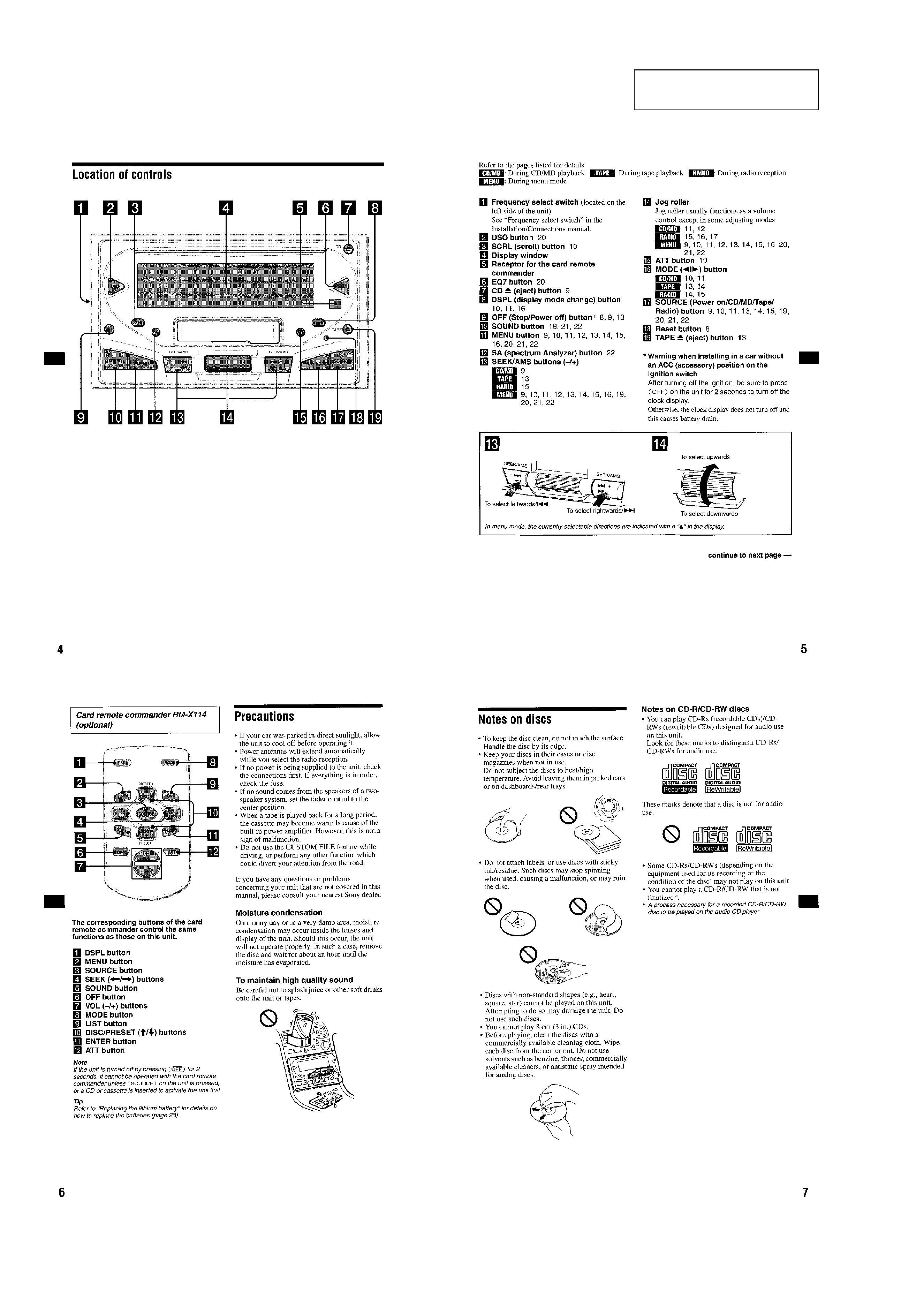
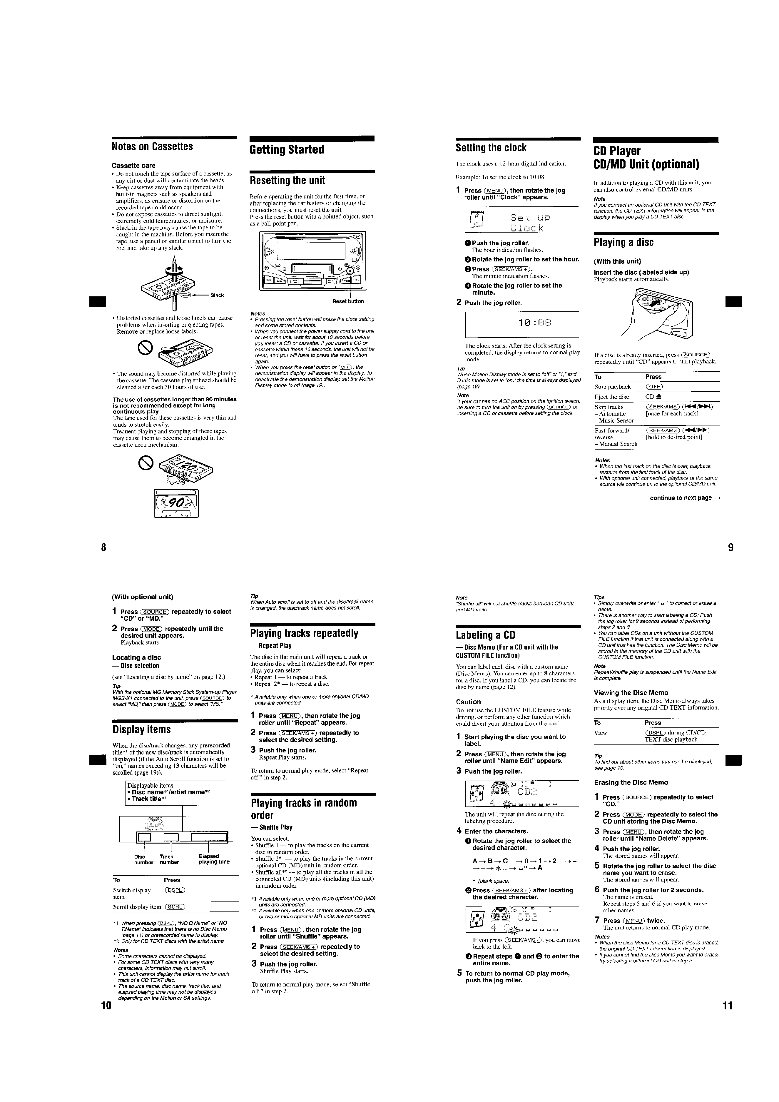
Location of Controls ............................................................... 4
Getting Started ........................................................................ 5
CD Player ............................................................................... 5
Cassette Player ....................................................................... 6
Radio ...................................................................................... 6
Other Functions ...................................................................... 7
Connections ............................................................................ 9
2. DISASSEMBLY
2-1. Front Panel Assy .............................................................. 11
2-2. CD Mechanism Block ...................................................... 12
2-3. CD Main Board ................................................................ 12
2-4. Tension Spring (FL) ......................................................... 13
2-5. Floating Block Assy ......................................................... 13
2-6. Roller Arm Assy ............................................................... 14
2-7. Optical Pick-up Assy ........................................................ 14
2-8. Chassis (Top) Assy ........................................................... 15
2-9. Main Board ...................................................................... 15
2-10. Heat Sink .......................................................................... 16
2-11. Tape Mechanism Block .................................................... 16
3. ASSEMBLY OF MECHANISM DECK
3-1. Housing ............................................................................ 17
3-2. Arm (Suction) ................................................................... 17
3-3. Lever (LDG-A)/(LDG-B) ................................................ 18
3-4. Gear (Loading FT) ........................................................... 18
3-5. Guide (U) ......................................................................... 19
3-6. Main Motor Assy ............................................................. 19
4. MECHANICAL ADJUSTMENTS .............................. 20
5. ELECTRICAL ADJUSTMENTS
Tape Section ......................................................................... 20
6. DIAGRAMS
6-1. IC Pin Descriptions .......................................................... 22
6-2. Block Diagram CD Section .......................................... 26
6-3. Block Diagram Tuner Section ...................................... 27
6-4. Block Diagram Tape Section ....................................... 28
6-5. Circuit Boards Location ................................................... 29
6-6. Printed Wiring Boards CD Mechanism Section ........... 30
6-7. Schematic Diagram CD Mechanism Section .............. 31
6-8. Printed Wiring Board Main Section ............................. 32
6-9. Schematic Diagram Main Section (1/3) ....................... 34
6-10. Schematic Diagram Main Section (2/3) ....................... 35
6-11. Schematic Diagram Main Section (3/3) ....................... 36
6-12. Printed Wiring Board Jog Section ................................ 37
6-13. Printed Wiring Board Display Section ......................... 38
6-14. Schematic Diagram Display, Jog Section .................... 40
7. EXPLODED VIEWS
7-1. Cover Section ................................................................... 46
7-2. Front Panel Section .......................................................... 47
7-3. Main Board Section ......................................................... 48
7-4. CD Mechanism Section (1) .............................................. 49
7-5. CD Mechanism Section (2) .............................................. 50
7-6. Tape Mechanism Section ................................................. 51
8. ELECTRICAL PARTS LIST ................................... 52
WX-4500X
4
WX-4500X
SECTION 1
GENERAL
This section extracted from
instruction manual.
5
WX-4500X