TMR-RF915R/RF945R
SERVICE MANUAL
TRANSMITTER
SPECIFICATIONS
US Model
Canadian Model
TMR-RF915R is the component model block one in the MDR-RF915RK.
TMR-RF945R is the component model block one in the MDR-RF945RK.
9-873-139-11
2001E0200-1
© 2001.5
Sony Corporation
Personal Audio Company
Shinagawa Tec Service Manual Production Group
Ver 1.0 2001. 05
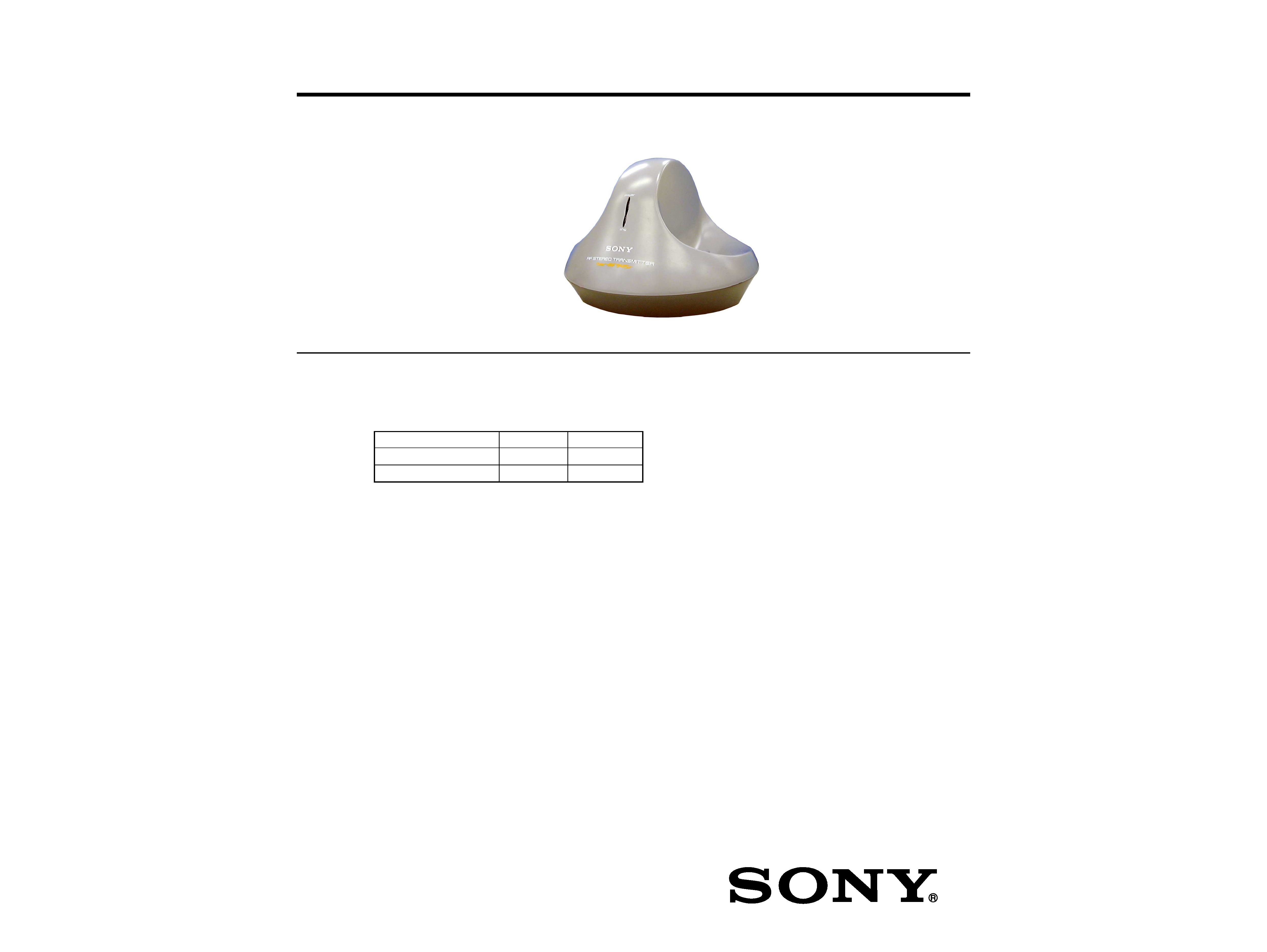
Photo : TMR-RF945R
MDR-RF915RK MDR-RF945RK
Wireless Stereo Headphones MDR-RF915R
MDR-RF945
Transmitter
TMR-RF915R
TMR-RF945
COMPONENT MODEL NAME FOR MDR-RF915RK/
MDR-RF945RK
General
Carrier frequency
913.5 914.5 MHz
Channel
Ch1, Ch2, Ch3
Modulation
FM stereo
Frequency response
20 20,000 Hz
Transmitter
Power source
DC 9 V: supplied AC power
adaptor
Audio input
phono jacks/stereo mini jack
Dimensions
Approx. 150 mm dia X 108 mm
(6 X 41/3 in.) (w/h)
Mass
Approx. 190 g (6.7 oz.)
Design and specifications are subject to change without
notice.
2
TMR-RF915R/RF945R
SECTION 1
GENERAL
Setting up the
transmitter
1 Connect the transmitter to audio/video
equipment. Select one of the hookups
below depending on the jack type:
To connect to a headphones jack
DC IN 9V
OFF ON
FILTER
NOISE
12 3
CHANNEL
R
BA
L
AUDIO IN
Transmitter
Left channel
(white)
Right channel
(red)
Unimatch plug
adaptor
(supplied)
Discman, MD,
WALKMAN*, VCR,
etc.
to headphones
jack (stereo
mini jack)
Connecting cord
(supplied)
to AUDIO IN
A jacks
to headphones
jack (stereo
phone jack)
A
1.
Check the area of your repair for unsoldered or poorly-sol
deredconnections. Check the entire board surface for solder
splashes and bridges.
2.
Check the interboard wiring to ensure that no wires are
"pinched" or contact high-wattage resistors.
3.
Look for unauthorized replacement parts, particularlyt ransis
tors, that were installed during a previous repair.
Point them out to the customer and recommend their
replacement.
4.
Look for parts which, through functioning, show obvious
signs of deterioration. Point them out to the customer and
recommend their replacement.
SAFETY CHECK-OUT
After correcting the original service problem, perform the following
safety checks before releasing the set to the customer.
5.
Check the B+ voltage to see it is at the values specified.
6.
Flexible Circuit Board Repairing
· Keep the temperature of the soldering iron around 270
°C
during repairing.
· Do not touch the soldering iron on the same conductor of
the circuit board (within 3 times).
· Be careful not to apply force on the conductor when
soldering
TABLE OF CONTENTS
Specifications ............................................................................ 1
1. GENERAL ...................................................................... 2
2. DISASSEMBLY
2-1. Cabinet (Upper) ........................................................ 3
2-2. TX-BASE Board ....................................................... 3
3. ELECTRICAL ADJUSTMENTS ............................. 4
4. DIAGRAMS
4-1. Block Diagrams ......................................................... 5
4-2. Schematic Diagram ................................................... 6
4-3. Printed Wiring Board ................................................ 7
5. EXPLODED VIEWS..................................................... 8
6. ELECTRICAL PARTS LIST...................................... 9
This section is extracted from
instruction manual.
3
TMR-RF915R/RF945R
SECTION 2
DISASSEMBLY
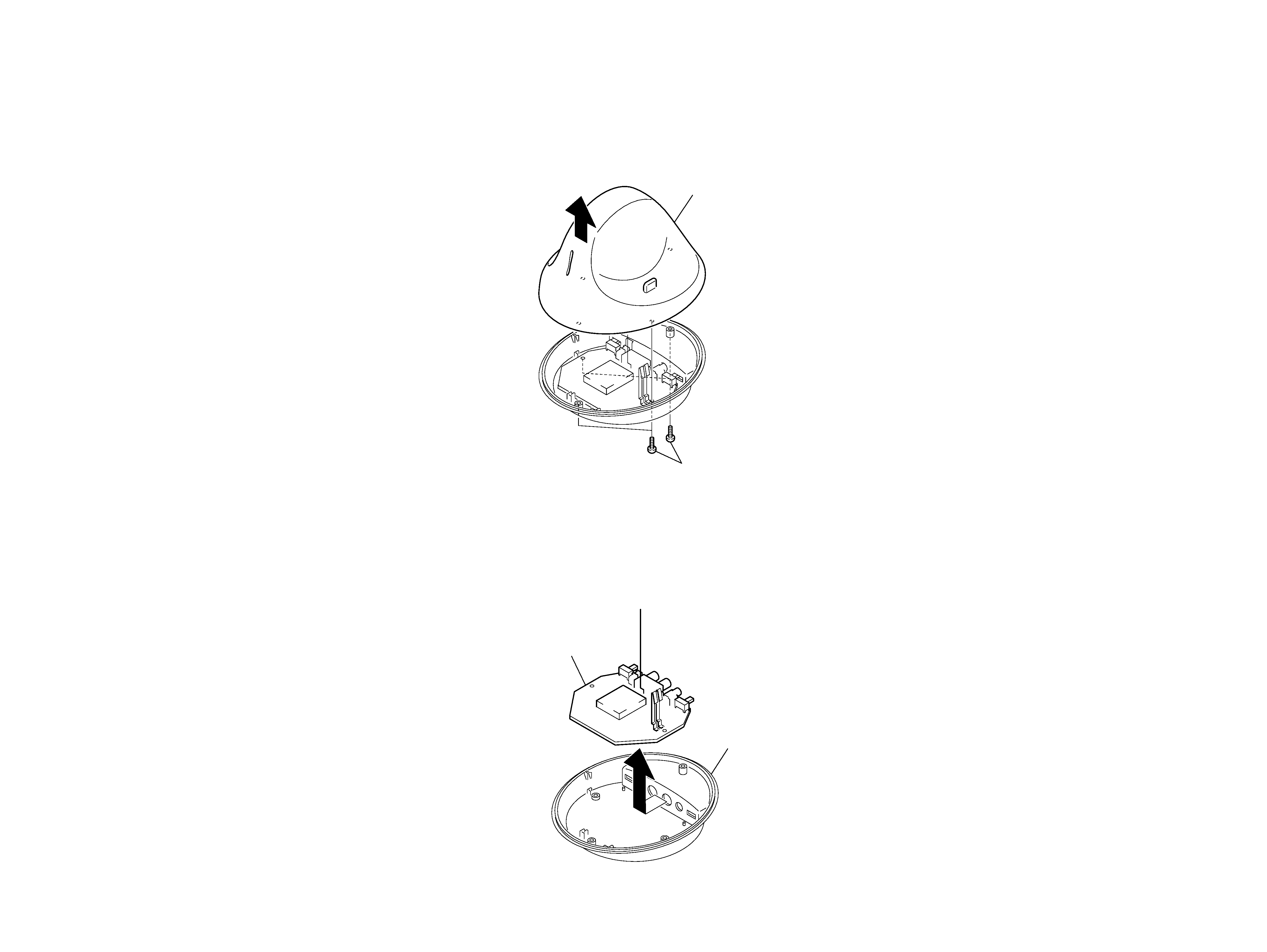
2-1. CABINET (UPPER)
· This set can be disassembled in the order shown below.
1
Four screws (P 2
× 8)
Cabinet (upper)
2
2-2. TX-BASE BOARD
2
TX-BASE board
Cabinet assy, lower
1
4
TMR-RF915R/RF945R
SECTION 3
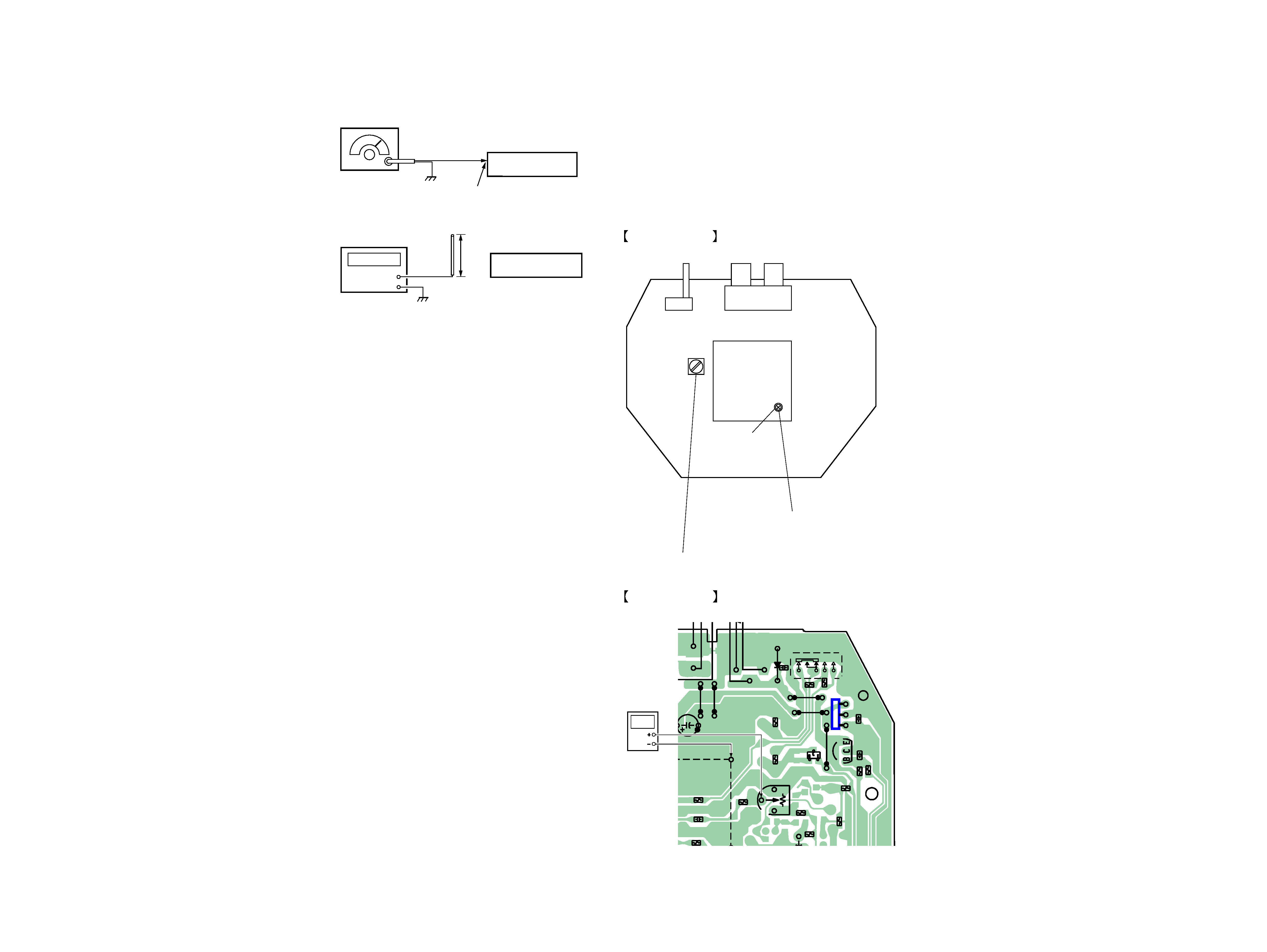
ELECTRICAL ADJUSTMENTS
Transmission Frequency Check
1. Set the noise filter SW to OFF.
2. Input a signal of 1 kHz 40 mVrms to only the L-CH (J402).
3. Connect a telescopic antenna to the frequency counter input
and extend the antenna to a length of approximately 8 cm.
4. Place TX-BASE board close to the frequency counter, then mea-
sure the frequencies of CH1, CH2 and CH3 and make sure the
values are as follows:
CH1 : 913.5 MHz
± 200 kHz
CH2 : 914.0 MHz
± 200 kHz
CH3 : 914.5 MHz
± 200 kHz
When the frequency is not satisfied the specified value, set the
channel switch (S402) to CH2, then adjust the value of the
frequency counter to 914.0 MHz by trimmer capacitor in the VCO
unit.
Standard value :913.9MHz to 914.1MHz
When completed with replacement, recheck the
frequencies of CH1, CH2 and CH3.
Setting :
AF signal
generator
Telescopic
antenna
8 cm
L-CH (J402)
TMR-RF915R/RF945R
set
TMR-RF915R/RF945R
set
Frequency counter
Pilot signal Modulation Check and Adjustment
1. Set the channel to CH2.
2. An electric wave is output for 5or 10 minutes when OFF to ON a
power supply (Power indicator will ON).
3. Measure the center terminal of RV403 using an digital volt-meter
(AC range) and make sure the value is 2 to 2.5mVrms.
If the measured value is other than the specified value, adjust to
2 to 2.5mVrms by turning the RV403 on the TX-BASE board.
Connection points and Adjustment Location :
(Component side)
S402
Hole
J402
(L-CH) (R-CH)
CH3
CH2 CH1
RV403: Modulation adjustment
Trimmer : Transmission
frequency adjustment
VCO UNIT
RV403
R449
R466
R464
R472
R489
JC430
Q408
R482
CO401
O UNIT)
C480
C468
C475
R484
C439
R485
R483
R486
JC470
R481
C470
JW
417
JW
420
58
IC402
D403
JW415
JW416
Q404
JW
413
RV403
1
2
3
digtal voltmeter
(AC range)
(Conductor side)
TX-BASE BOARD
TX-BASE BOARD
5
5
TMR-RF915R/RF945R
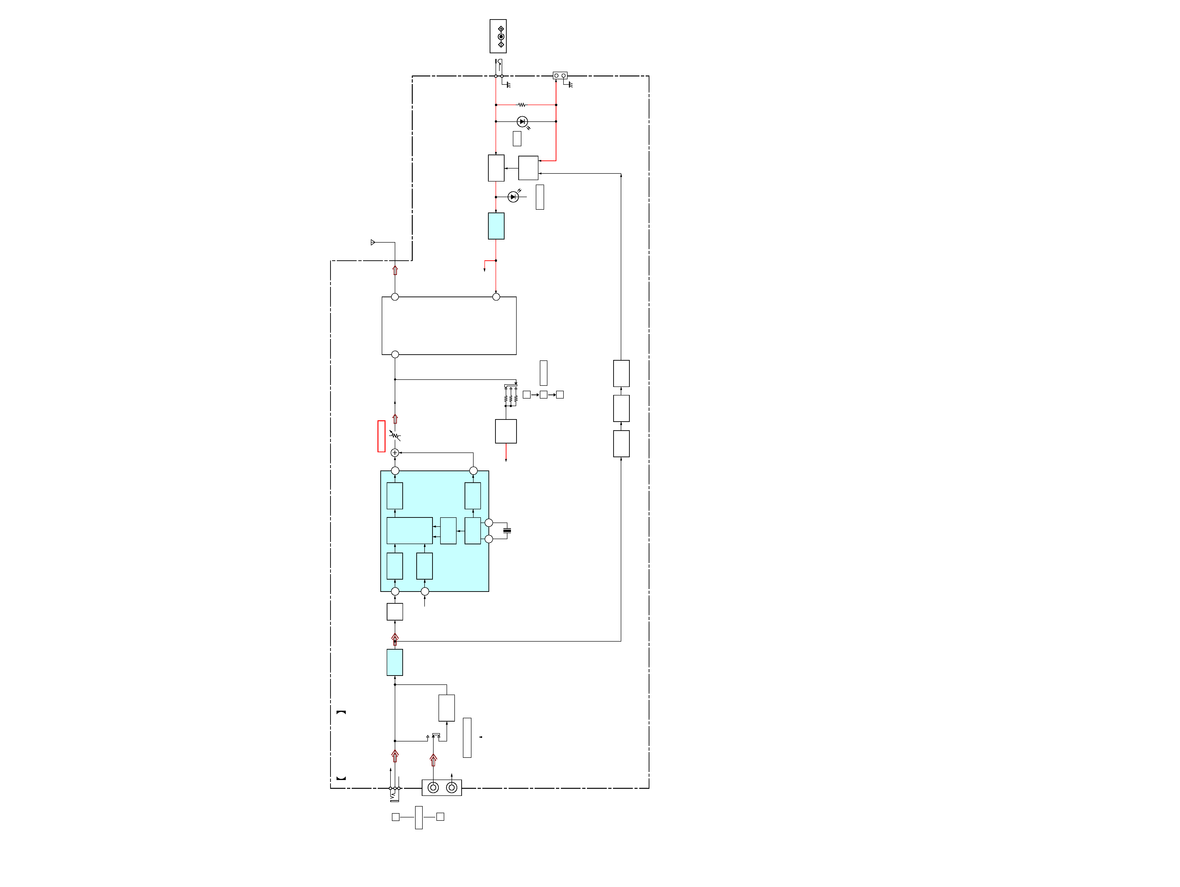
J401
S401
NOISE FILTER
NOISE
FILTER
ALC
AMP
CH1
AMP
BUFFER
BUFFER
Q401
RECT
D404,405
INPUT
DET
DIVIDER
BUFFER
OSC
AMP
TIME
DEVISION
MPX
J402
OFF
|
ON
L
R
R-CH
R-CH
R-CH
1
9
8
7
6
CH2
AMP
14
X401
38kHz
RV403
IC401
LPF
IC403
STEREO MPX
+5V
REG
SWITCH
Q404
IC402
ANT401
D401
D402
POWER
CHG
AUDIO IN
B
A
TX-BASE BOARD
MOD IN
ANT
5V
B+
5V
VCO401
(VCO UNIT)
I
O
V
MODULATION
CHANNEL
SET
Q408
S402
CHANNEL
1
2
B+
5V
3
Q402,405
CHARGE
TERMINAL
(TO MDR-RF915R/RF945R)
+
J404
DC IN 9V
POWER
ON/OFF
Q406,407
· R-ch is omitted due to same as L-ch.
· Signal path.
L
: AUDIO
F
: FM
4-1. BLOCK DIAGRAMS
SECTION 4
DIAGRAMS