TMR-RF830R is the component model block one in MDR-RF830RK.
COMPONENT MODEL NAME FOR MDR-RF830RK
TMR-RF830R
AEP Model
UK Model
SERVICE MANUAL
TRANSMITTER
MICROFILM
SPECIFICATIONS
General
Carrier frequency
863.32 863.67 MHz
Channel
Ch1, Ch2
Modulation
FM stereo
Frequency response
20 20,000 Hz
Transmitter
Power source
DC 9 V: supplied AC power adaptor
Audio input
phono jacks/stereo mini jack
Dimensions
Approx. 120 mm dia
× 290 mm
(43/4
× 111/2 in.)(w/h)
Mass
Approx. 155 g (5.5 oz.)
Design and specifications are subject to change
without notice.
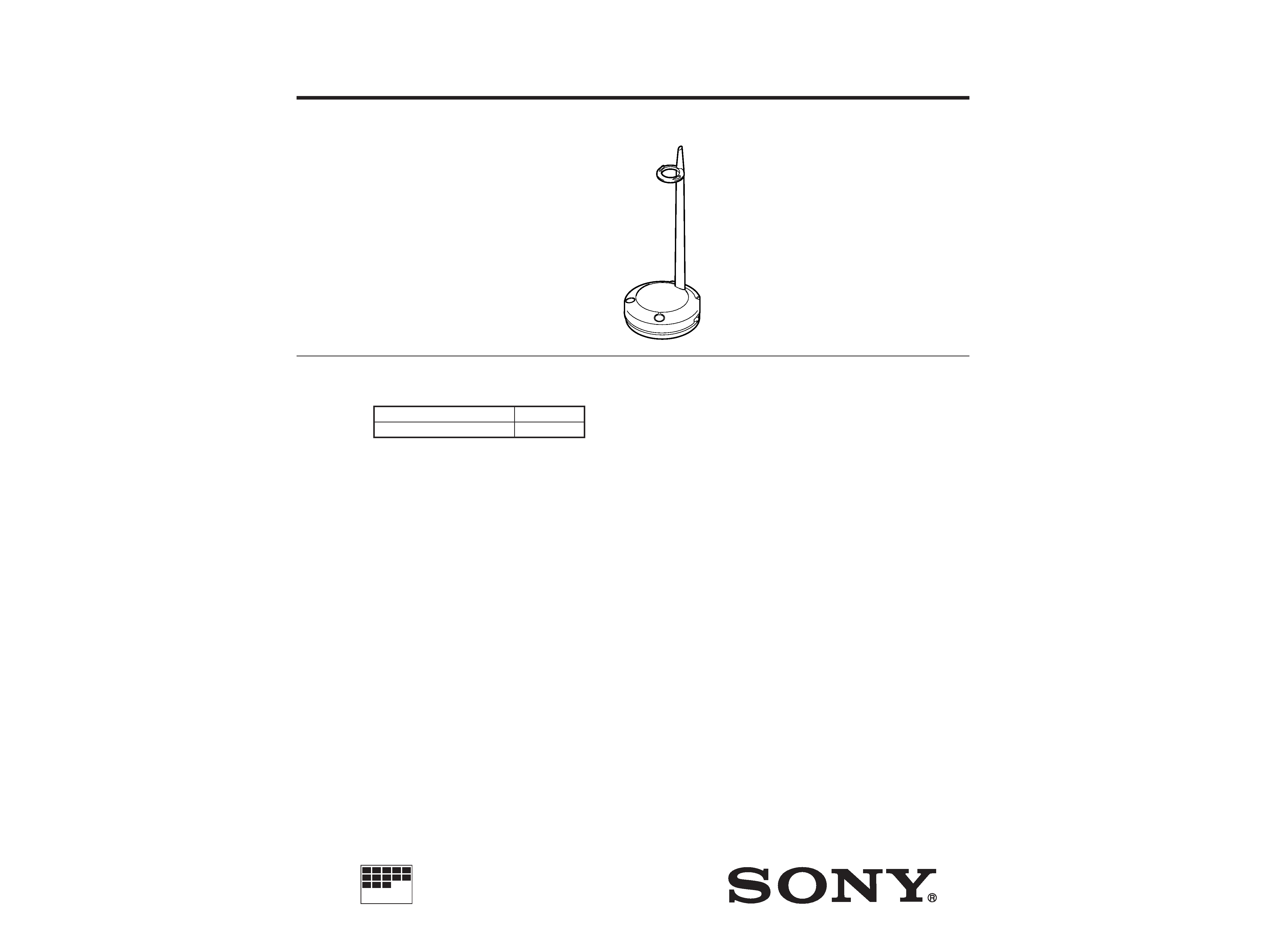
Wireless Stereo Headphones
MDR-RF830
Transmitter
TMR-RF830R
REVISED
Ver 1.2 1999. 09
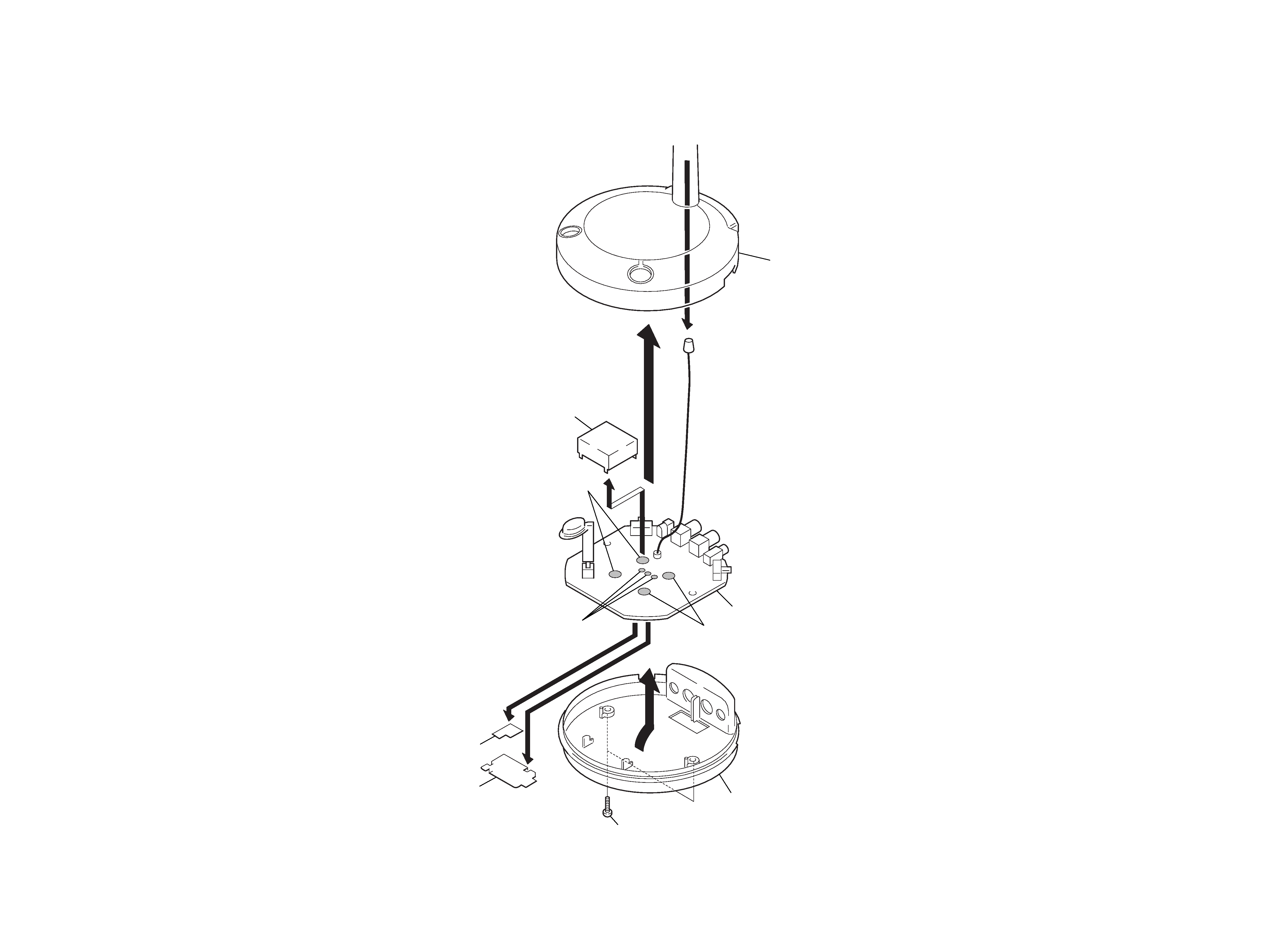
Note : Follow the disassembly procedure in the numerical order given.
SECTION 1
DISASSEMBLY
-- 2 --
1-1. TX BOARD, VCO BLOCK
Cabinet (Upper)
Vco block
7 Remove
solder
7 Remove solder
8 Remove solder
TX board
6 TX shield plate
5 TX shield plate
1 Screws +P2
× 10
Cabinet (Lower)
9
2
4
3
TMR-RF830R
Note :
1.
The transmitter section adjustments should be completed before per-
forming the headphones section adjustment.
2.
On adjusting the transmitter section, use the headphones as a jig.
SECTION 2
ELECTRICAL ADJUSTMENTS
-- 3 --
-- 4 --
Send Frequency Check and Adjustment
1. Set the noise filter SW to OFF.
2. Input a signal of 1 kHz 40 mVrms to only the L-CH (J403).
3. Connect a telescopic antenna to the frequency counter input
and extend the antenna to a length of approximately 8 cm.
4. Place TX board close to the frequency counter, then measure
the frequencies of CH1 and CH2 and make sure the values are
as follows:
CH1 : 863.27 to 863.37 MHz
CH2 : 863.62 to 863.72 MHz
When the frequency is not satisfied the specified value, first
set the channel switch (S402) to "2" and adjust CH2 frequency
with L412, next set it to "1" and adjust CH1 frequency with
L413. When completed with adjustment, recheck the frequecies
of CH1 and CH2.
Main-Carrier (L+R) Modulation Check and Adjustment
1. Set the noise filter SW to off.
2. Set the channel to CH2.
3. Input a signal of 1 kHz 316 Vrms to the L-ch (J403) and the R-
CH.(J402)
4. Measure the pin 2 voltage of the TX board RV 404 using a
digital voltmeter (AC range) and make sure the value is 75 to
95 mVrms. If the measured value is other than the specified
value, adjust to 85mVrms by turning the RV 404 on the TX
board.
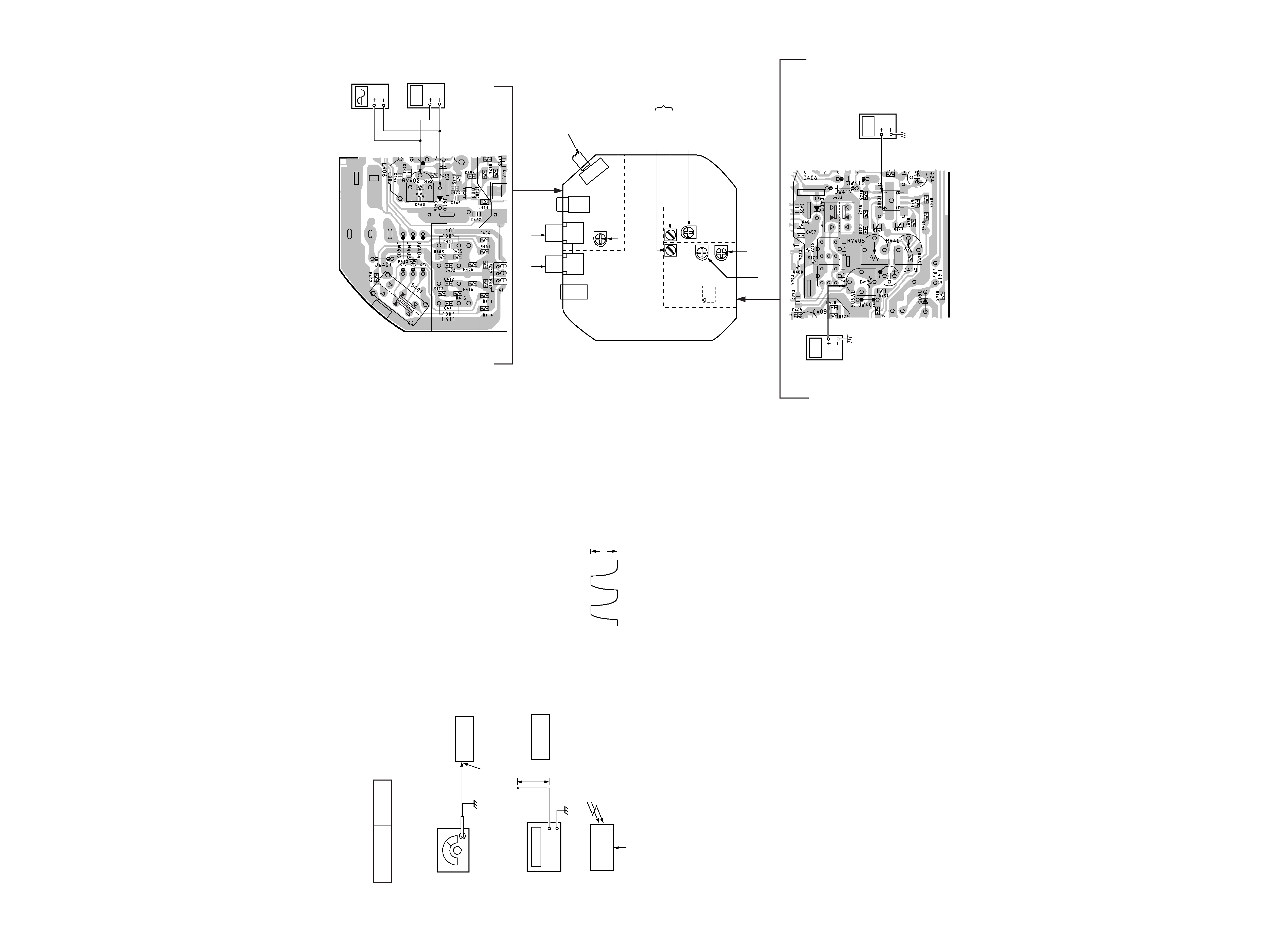
Connection points and Adjustment Location :
TX board (See page 4)
[TX BOARD] (Component side)
Sub-Carrier (L-R) Modulation Check and Adjustment
1. Set the noise filter SW to OFF.
2. Set the channel to CH2.
3. Input a signal of 1 kHz 316 mVrms to the L-CH (J403).
4. Measure the pin 1 voltage of the TX board IC403 using an
digital voltmeter (AC range) and make sure the value is 220 to
250 mVrms. If the measured value is other than the specified
value, adjust to 235mVrms by turning the RV401 on the TX
board.
Connection points and Adjustment Location :
TX board (See page 4)
Sub-Carrier Frequency/Level Check and Adjustment
1. Set the noise filter SW to OFF.
2. Set the channel to CH2.
3. Input a signal of 1 kHz 316 mVrms to only the L-CH (J403).
4. Connect a frequency counter and an oscilloscope between the
pin 2 of RV402 and GND.
5. Set the TX board L-CH (J403) input to OFF (not doing so will
cause modulation in the sub-carrier, preventing correct mea-
surement)
6. Check to make sure the frequency counter reading is 49 to
51kHz. If the measured value is other than the specified value,
adjust the frequency to 50 kHz by turning the RV405 on the TX
board. In addition, check to make sure the oscilloscope wave-
form is as follows :
Headphones
MDR-RF830
80 100mVp-p
13
4
5
-1
-2
Frequency counter
Oscilloscope
Sub-Carrier
Frequency
Adjustment
RV402
L412 (CH2)
L413 (CH1)
S401
Noise Filter ON/OFF Switch
J402
(R-CH)
RV404 : Main-Carrier (L+R)
Modulation Adjustment
RV401 : Sub-Carrier (L R) Modulation Adjustment
RV405 : Sub-Carrier Frequency Adjustment
Send Frequency
Adjustment
J403
(L-CH)
Sub-Carrier Level Adjustment
1
-1
-2
2
CHANNEL
Digital voltmeter
(AC range)
Main-Carrier (L+R)
Modulation Adjustment
Sub-Carrier (L-R)
Modulation Adjustment
Digital voltmeter
(AC range)
Transmitter
TMR-RF830R
Setting :
7. When the waveform P-P level is not satisfied the specified value,
adjust to 90mVp-p with RV402.
(Perform the check and adjustment within one minute since the
transmitter AUTO OFF function will be activated approximately
one minute after setting the transmitter L-ch input to OFF. If
the AUTO OFF function activates, set the L-ch input to ON, set
TX board to AUTO ON, set the L-ch input again to OFF, then
make the check adjustment.)
Connection points and Adjustment Location :
TX board (See page 4)
AF signal
generator
Telescopic
antenna
8 cm
L-CH (J403)
TMR-RF830R
set
TMR-RF830R
set
Frequency counter
MDR-RF830
Headphones
Battery terminal (DC 3V)
TMR-RF830R
-- 5 --
-- 6 --
Note:
· X : parts extracted from the component side.
·
p
: parts mounted on the conductor side.
·
®
: Through hole.
· b : Pattern from the side which enables seeing.
Caution:
Pattern face side:
Parts on the pattern face side seen from
(SideB)
the pattern face are indicated.
Parts face side:
Parts on the parts face side seen from
(Side A)
the parts face are indicated.
SECTION 3
DIAGRAMS
12
A
B
C
D
E
F
G
H
I
3456789
10
3-1. PRINTED WIRING BOARD
Ref. No.
Location
D401
B-6
D402
B-7
D404
E-7
D405
E-7
D406
B-5
D407
C-5
D408
D-5
D409
D-6
D410
C-6
D411
E-4
IC401
F-6
IC402
C-6
IC403
C-7
IC404
D-5
IC405
E-4
Q401
F-7
Q403
B-5
Q404
B-5
Q405
B-4
Q406
C-6
Q407
C-4
Q408
C-4
Q409
C-3
· Semiconductor
Location
1-670-641-
11
(11)
TX BOARD
DC IN 9V
J404
1
-1
-2
-1
-2
2
2
3
OFF
ON
OFF
ON
POWER
CHANNEL
13
4
5
-1
-2
S401
NOISE
FILTER
ANT401
FM
WIRE
ANTENNA
L408
AUDIO
IN
L
R
B
A
J403
J402
J401
RECHARGEABLE
BATTERY
Ni-Cd NC-AA(HJ) x 2
CHARGE TERMINAL
16
1
2
3
NOTE:
THE VCO BLOCK IS SUPPLIED
AS A UNIT FOR SERVICE.
3
2
1
VCO BLOCK
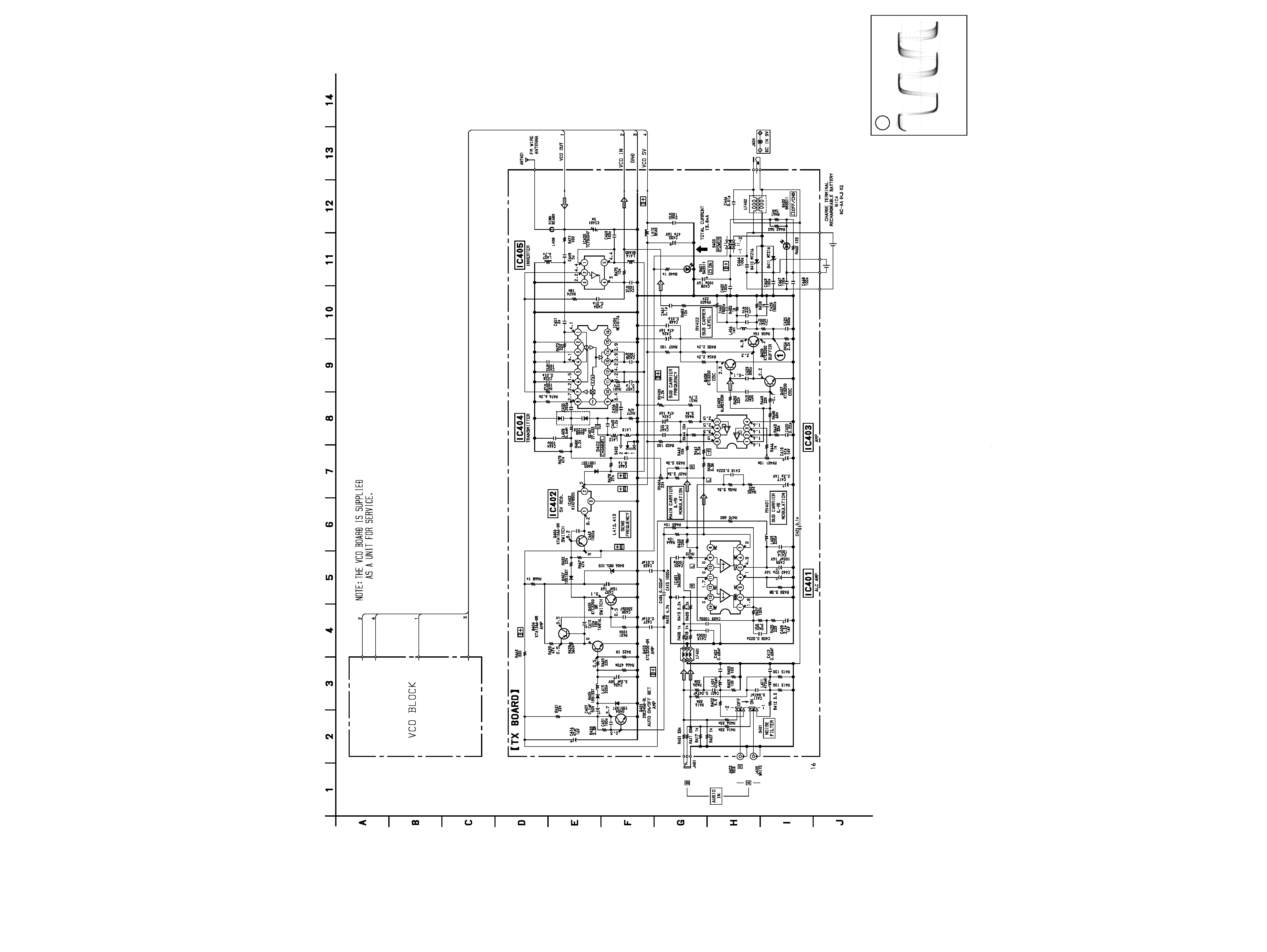
TMR-RF830R
Note on Schematic Diagram:
· All capacitors are in
µF unless otherwise noted. pF: µµF 50 WV
or less are not indicated except for electrolytics and tantalums.
· All resistors are in
and 1/4 W or less unless otherwise speci-
fied.
·
¢
: internal component.
· U : B+ Line.
· H : adjustment for repair.
·Power voltage is dc 3 V and fed with regulated dc power supply
from battery terminal.
-- 7 --
-- 8 --
r WAVEFORM
1
VOLT/DIV : 0.2m V AC
TIME/DIV : 10
µsec
3-2. SCHEMATIC DIAGRAM
·Voltages are dc with respect to ground under no-signal conditions.
·Voltages are taken with a VOM (Input impedance 10 M
).
Voltage variations may be noted due to normal production tolerances.
·Waveforms are taken with a oscilloscope.
Voltage variations may be noted due to normal production tolerances.
· Circled numbers refer to waveforms.
· Signal path.
F