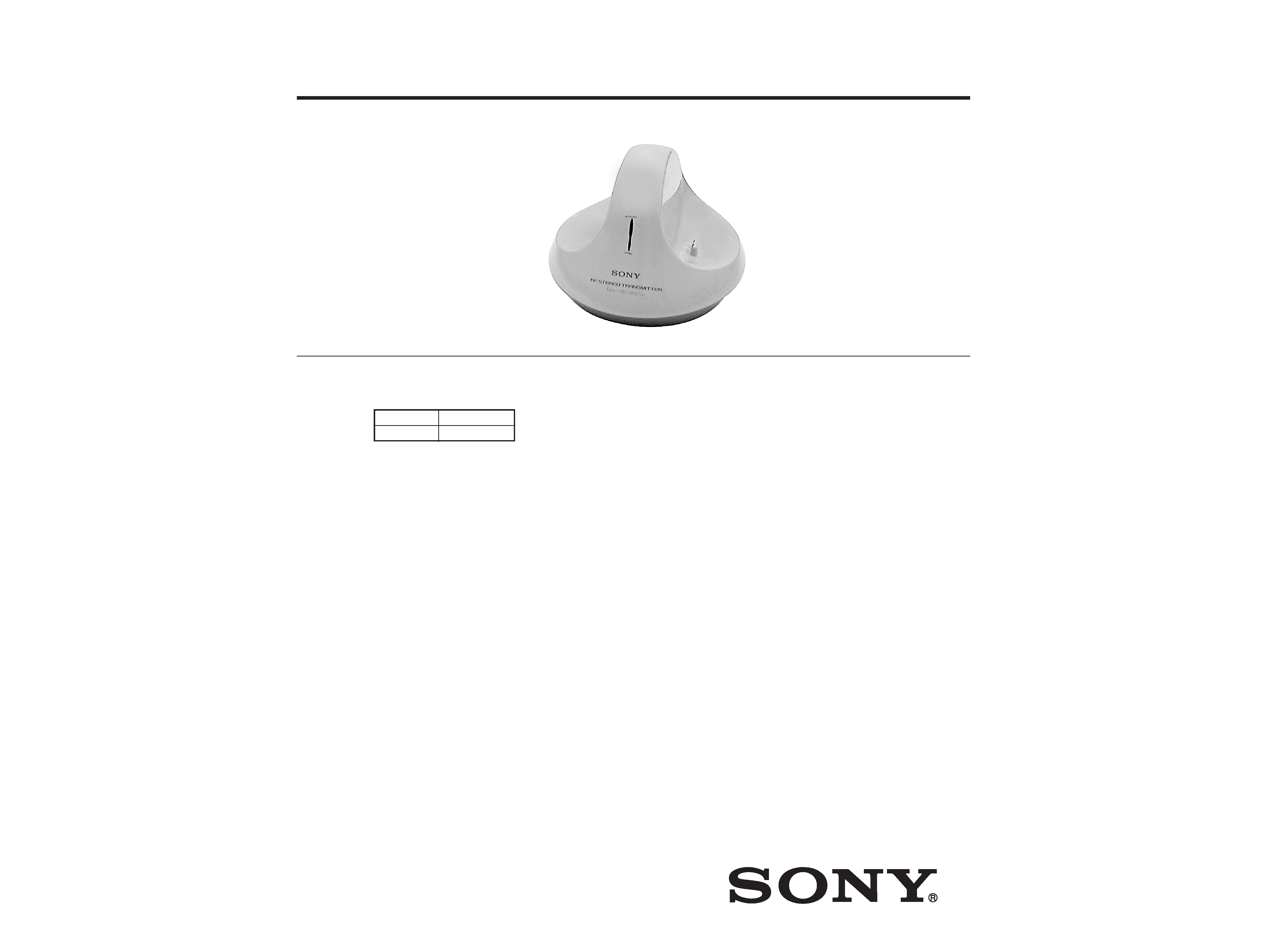
TMR-RF815R
AEP Model
UK Model
SERVICE MANUAL
TRANSMITTER
SPECIFICATIONS
Headphones
MDR-RF815R
Transmitter
TMR-RF815R
TMR-RF815R is the component model block one in the MDR-RF815RK.
COMPONENT MODEL NAME FOR MDR-RF815RK
General
Carrier frequency
863.5 864.5 MHz
Channel
Ch1, Ch2, Ch3
Modulation
FM stereo
Frequency response
20 20,000 Hz
Transmitter
Power source
DC 9 V: supplied AC power
adaptor
Audio input
phono jacks/stereo mini jack
Dimensions
Approx. 150 mm dia
× 108 mm
(6
× 4 1/3 in.) (w/h)
Mass
Approx. 190 g (6.2 oz.)
Design and specifications are subject to change without
notice.
Ver 1.0 2000. 06
-- 2 --
SECTION 1
GENERAL
DC IN 9V
OFF ON
FILTER
NOISE
12 3
CHANNEL
R
BA
L
AUDIO IN
Setting up the
transmitter
1 Connect the transmitter to audio/video
equipment. Select one of the hookups
below depending on the jack type:
A
To connect to a headphones jack
Transmitter
Left channel
(white)
Right channel
(red)
Unimatch plug
adaptor
(supplied)
CD Walkman,
MD Walkman,
WALKMAN*,
VCR, etc.
to headphones
jack (stereo
mini jack)
Connecting cord
(supplied)
to AUDIO IN
A jacks
to headphones
jack (stereo
phone jack)
This section is extracted
from instruction manual.
1.
Check the area of your repair for unsoldered or poorly-
soldered connections. Check the entire board surface
for solder splashes and bridges.
2.
Check the interboard wiring to ensure that no wires are
"pinched" or contact high-wattage resistors.
3.
Look for unauthorized replacement parts, particularly
transistors, that were installed during a previous repair.
Point them out to the customer and recommend their
replacement.
4.
Look for parts which, through functioning, show obvious
signs of deterioration. Point them out to the customer
and recommend their replacement.
5.
Check the B+ voltage to see it is at the values specified.
6.
Flexible Circuit Board Repairing
· Keep the temperature of the soldering iron around 270°C
during repairing.
· Do not touch the soldering iron on the same conductor
of the circuit board (within 3 times).
· Be careful not to apply force on the conductor when
soldering
SAFETY CHECK-OUT
After correcting the original service problem, perform the following
safety checks before releasing the set to the customer.
-- 3 --
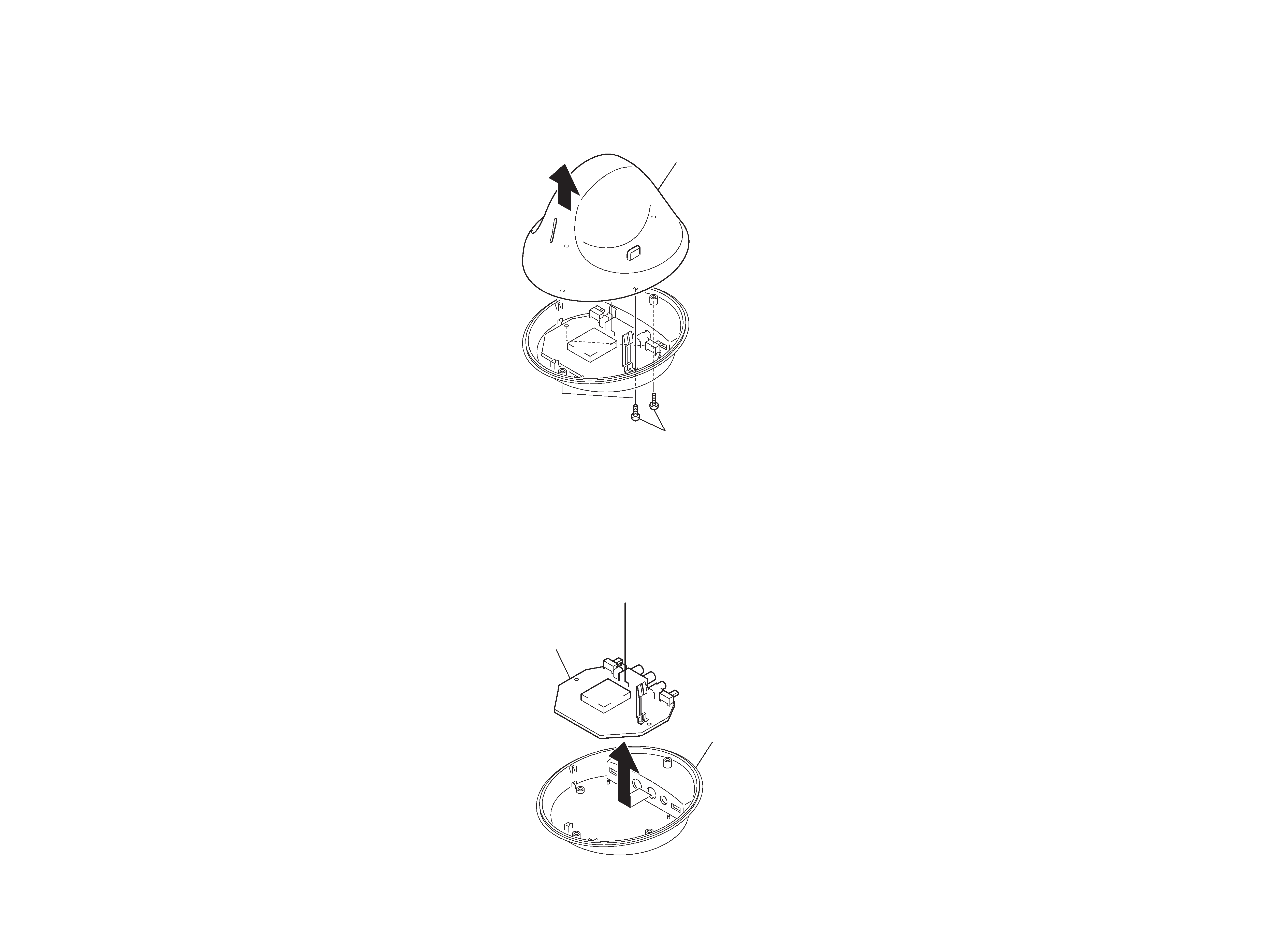
SECTION 2
DISASSEMBLY
2-1. CABINET (UPPER)
2-2. TX-BASE BOARD
1
Four screws (P 2
× 8)
Cabinet (upper)
2
2
TX-BASE board
Cabinet assy, lower
1
Note :
Follow the disassembly procedure in the numerical order given.
-- 4 --
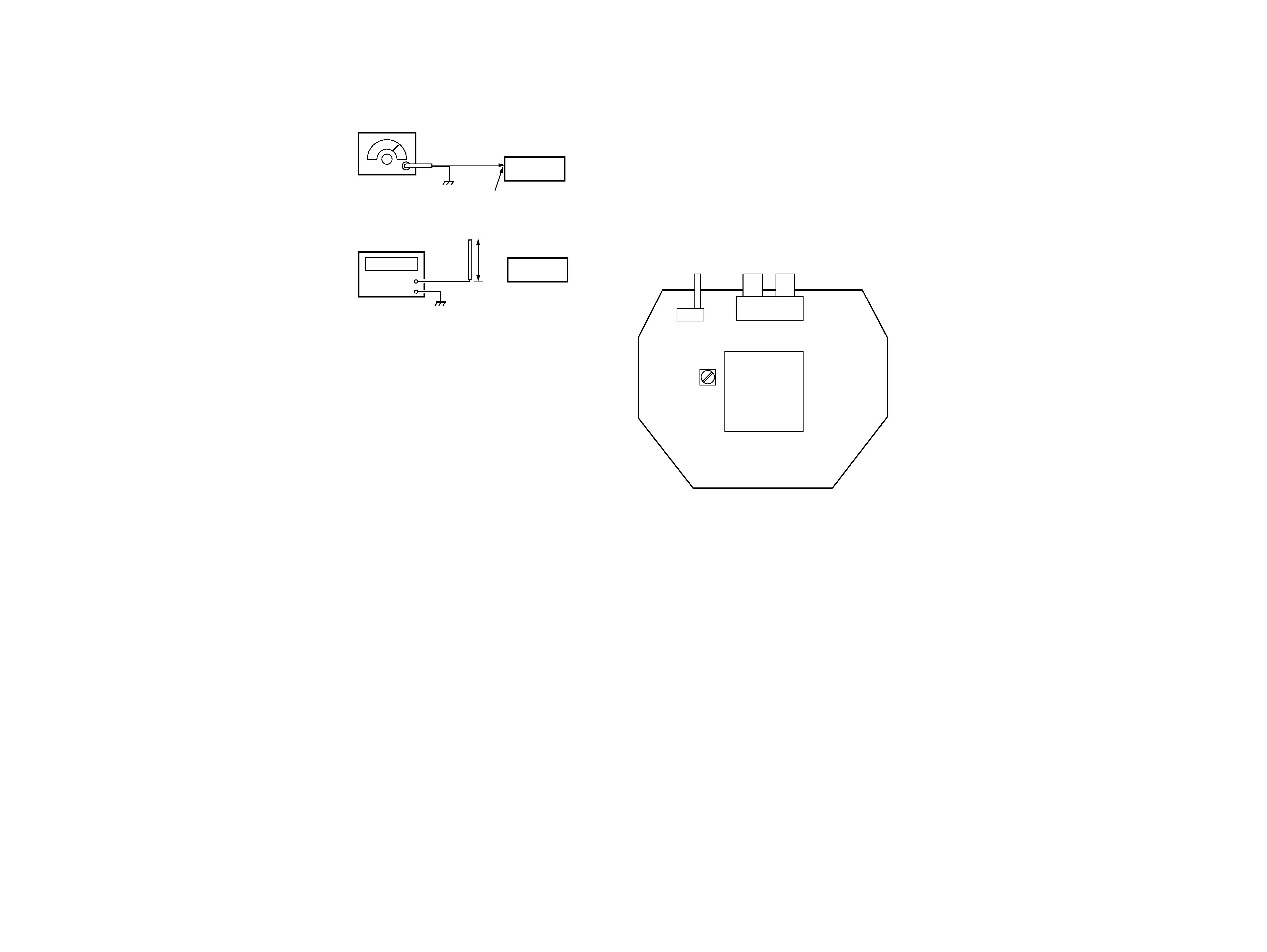
Setting :
SECTION 3
ELECTRICAL ADJUSTMENTS
Send Frequency Check
1. Set the noise filter SW to OFF.
2. Input a signal of 1 kHz 40 mVrms to only the L-CH (J402).
3. Connect a telescopic antenna to the frequency counter input
and extend the antenna to a length of approximately 8 cm.
4. Place TX-BASE board close to the frequency counter, then mea-
sure the frequencies of CH1, CH2 and CH3 and make sure the
values are as follows:
CH1 : 863.5 MHz ± 40 kHz
CH2 : 864.0 MHz ± 40 kHz
CH3 : 864.5 MHz ± 40 kHz
When the frequency is not satisfied the specified value, exchange
vco unit. When completed with replacement, recheck the
frequecies of CH1, CH2 and CH3.
[TK-BASE BOARD] (Component side)
AF signal
generator
Telescopic
antenna
8 cm
L-CH (J402)
TMR-RF815R
set
TMR-RF815R
set
Frequency counter
Pilot signal Modulation Check and Adjustment
1. Set the channel to CH2.
2. No signal input (The operating time in this case is limited to 4
or 5 minutes.)
3. Measure the movable terminal of RV403 using an digital volt-
meter (AC range) and make sure the value is 1.6mVrms ± 0.1mV.
If the measured value is other than the specified value, adjust to
1.6mVrms ± 0.1mV by turning the RV403 on the TX-BASE
board.
Connection points and Adjustment Location :
S402
J402
(L-CH) (R-CH)
CH3
CH2 CH1
VCO UNIT
RV403
TMR-RF815R
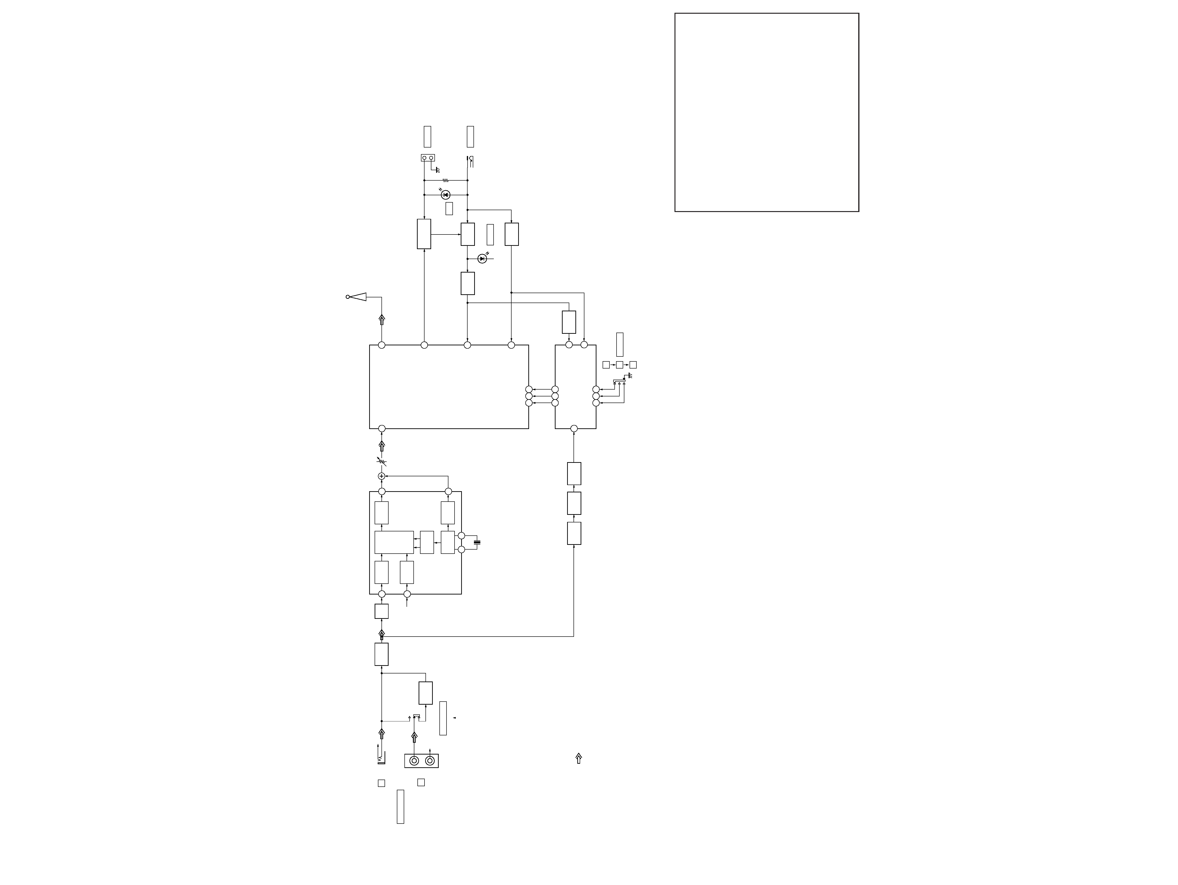
4-1. BLOCK DIAGRAM
-- 5 --
-- 6 --
SECTION 4
DIAGRAMS
J401
S401
NOISE FILTER
NOISE
FILTER
INPUT
AMP
CH1
AMP
BUFFER
BUFFER
Q401
RECT
D404,405
2V
D408
INPUT
DET
DIVIDER
BUFFER
OSC
AMP
TIME
DEVISION
MPX
AUDIO IN
B
J402
A
OFF
|
ON
S402
CHANNEL
L
R
R-CH
R-CH
R-CH
1
9
8
13
10
12
11
6
7
9
15
7
6
CH2
AMP
14
X401
38kHz
RV403
MOD IN
CE DI CL
CE DI CL
VS
16
5V
VCO CONTROLLER
IC404
IC401
LPF
IC403
STEREO MPX
IC405(1/2)
IC405(2/2)
+5V
REG
SWITCH
Q404
+4V
Q402
POWER OFF
DET
IC402
ANT
5V
B+
T-OUT
ANT401
D401
D402
J404
DC IN 9V
CHARGE
POWER
CHG
1
2
3
VCO UNIT
· Signal path.
: AUDIO
16
Note on Printed Wiring Board:
·
X : parts extracted from the component side.
·
b : Pattern from the side which enables seeing.
Note on Schematic Diagram:
· All capacitors are in µF unless otherwise noted. pF: µµF 50 WV or
less are not indicated except for electrolytics and tantalums.
· All resistors are in
and 1/4 W or less unless otherwise specified.
·
f
: internal component.
·
A : B+ Line.
·
H : adjustment for repair.
· Power voltage is dc 9 V and fed with regulated dc power supply
from battery terminal.
· Voltages are dc with respect to ground under no-signal conditions.
· Voltages are taken with a VOM (Input impedance 10 M
).
Voltage variations may be noted due to normal production toler-
ances.
· Waveforms are taken with a oscilloscope.
Voltage variations may be noted due to normal production toler-
ances.
· Circled numbers refer to waveforms.
· Signal path.
L: AUDIO