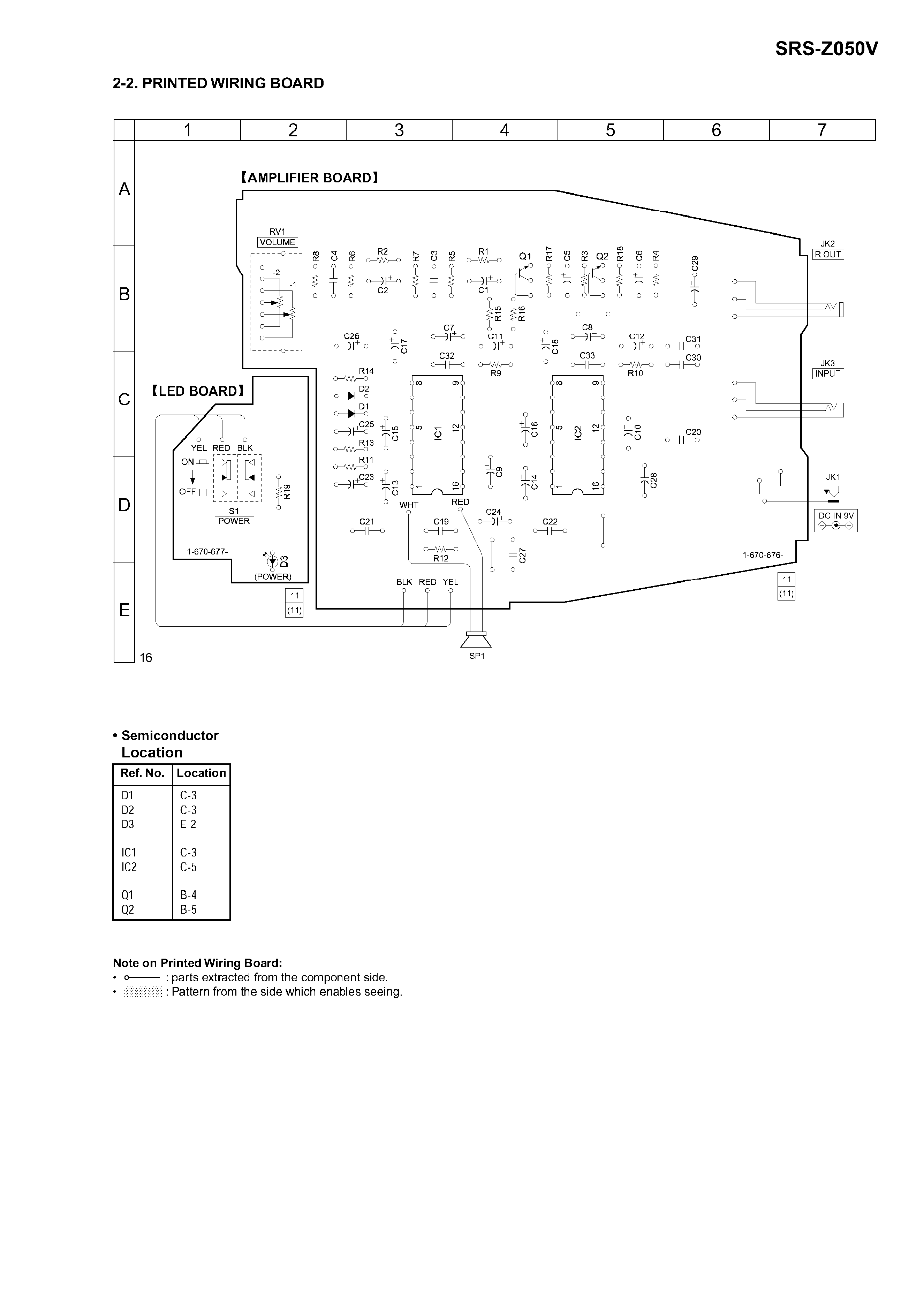
SECTION 2
DIAGRAMS
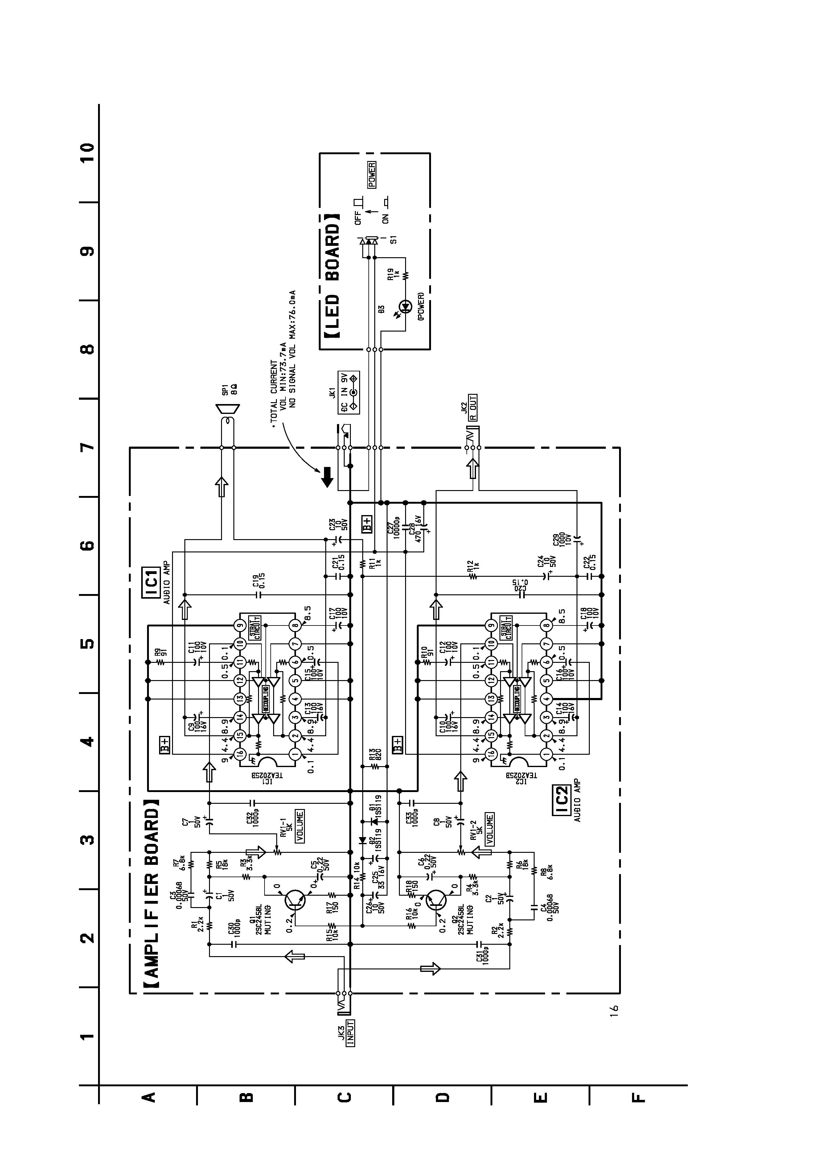
2-1. SCHEMATIC DIAGRAM
SRS-Z050V
Note on Schematic Diagram:
· All capacitors are in µF unless otherwise noted. pF: µµF
50 WV or less are not indicated except for electrolytics
and tantalums.
· All resistors are in
and 1/4 W or less unless otherwise
specified.
·
%
: indicates tolerance.
· C : panel designation.
· U : B+ Line.
· Power voltage is dc 9 V and fed with regulated dc power supply
from external power voltage jack.
· Voltages and waveforms are dc with respect to ground under no-
signal (detuned) conditions.
· Voltages are taken with a VOM (Input impedance 10 M
).
Voltage variations may be noted due to normal production toler-
ances.
· Signal path.
F
: AUDIO
-- 3 --
-- 4 --
204GD