MICROFILM
SERVICE MANUAL
CORDLESS TELEPHONE
US Model
Canadian Model
SPP-SS961
· SPP-SS961 is almost the same as SPP-SS960.
This service manual contains printed wiring boards, schematic diagrams, exploded views
and electrical parts list of this model.
Please refer to SPP-SS960 service manual (9-925-739-
) previously issued for other
information.
TABLE OF CONTENTS
1.
DIAGRAMS
1-1. Printed Wiring Boards BASE UNIT Section ..........
3
1-2. Schematic Diagram BASE UNIT Section ..............
5
1-3. Schematic Diagram HANDSET Section .................
8
1-4. Printed Wiring Board HANDSET Section .............. 11
2.
EXPLODED VIEWS ................................................ 13
3.
ELECTRICAL PARTS LIST ............................... 15
SPP-SS961
IC601
C-5
Q101
G-6
Q102
I-6
Q171
H-4
Q651
I-3
Q750
C-5
Q751
B-3
D100
B-5
D101
G-6
D102
D-7
D103
D-7
D104
G-6
D105
I-5
D108
E-2
D109
G-2
D110
F-3
D150
F-5
D654
I-1
IC101
I-5
IC150
E-5
IC602
G-3
IC701
F-2
IC751
D-2
3
4
1. DIAGRAMS
Caution:
Pattern face side: Parts on the pattern face side seen from the
(Side B)
pattern face are indicated.
Parts face side:
Parts on the parts face side seen from the
(Side A)
parts face are indicated.
Note:
· X : parts extracted from the component side.
· b : Pattern from the side which enables seeing.
(The other layers' patterns are not indicated.)
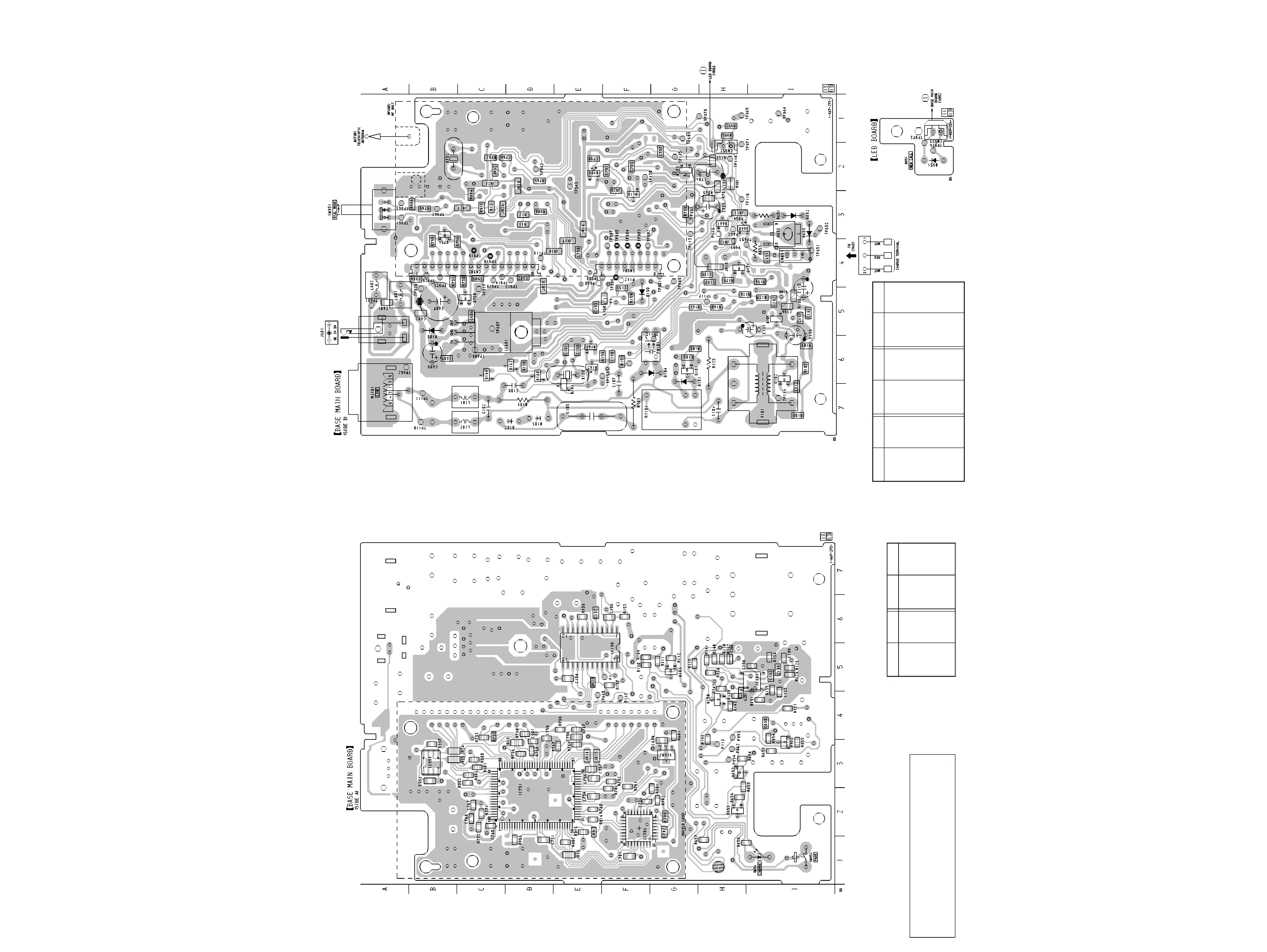
1-1.
PRINTED WIRING BOARDS BASE UNIT Section
Ref. No.
Location
· Semiconductor Location
BASE MAIN Board (Side B)
D160
D-6
D161
E-7
D162
E-6
D163
D-6
D164
C-6
D165
E-6
D652
I-3
D653
I-3
D660
H-3
D661
H-3
Ref. No.
Location
Ref. No.
Location
· Semiconductor Location
BASE MAIN Board (Side A)
IC951
B-3
Q103
G-5
Q150
H-4
Q652
H-3
Q653
H-2
Q952
I-3
Ref. No.
Location
Ref. No.
Location
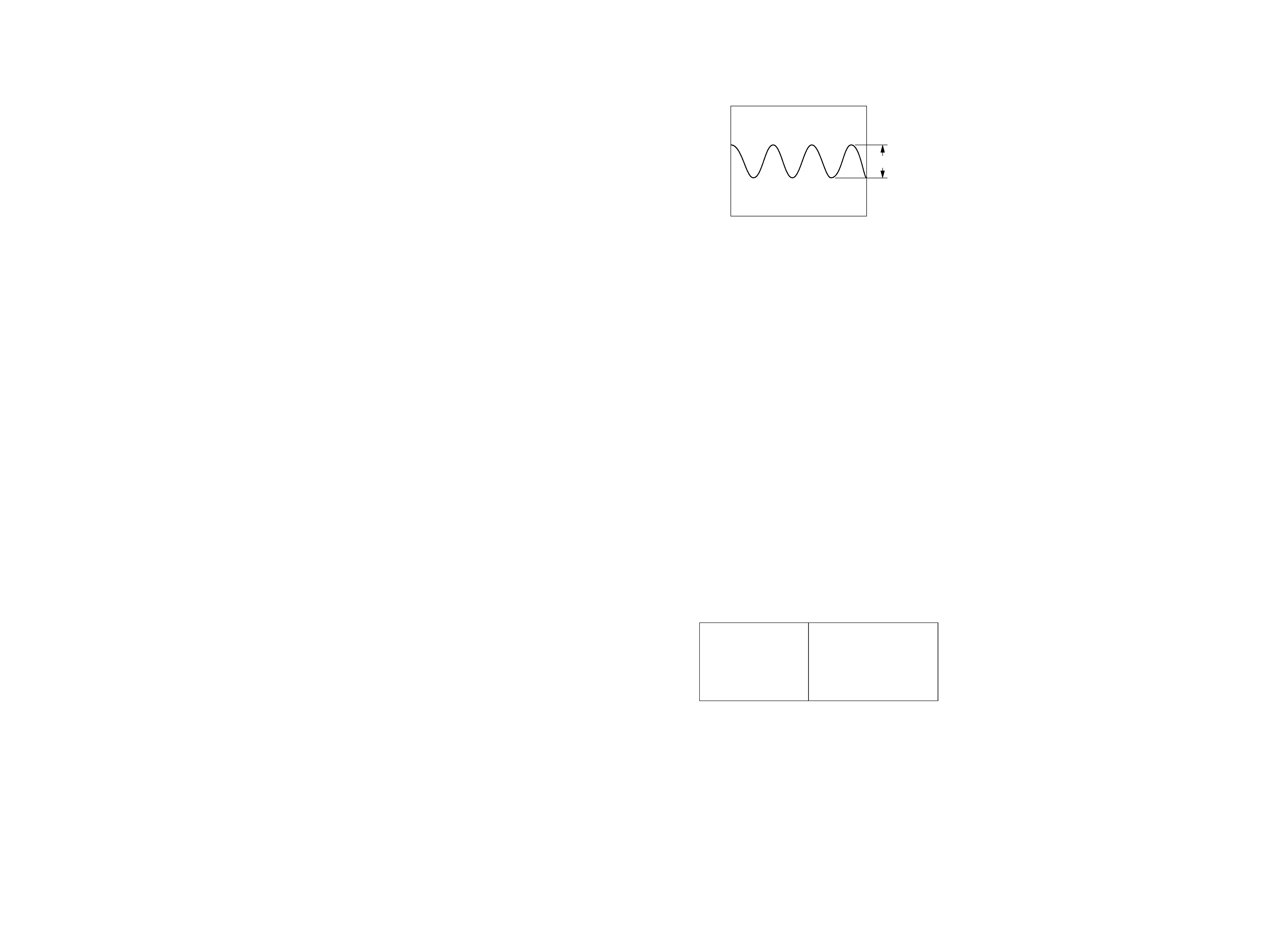
7
4 Vp-p
9.6 MHz
· Waveform
1 IC751 (¶ (XTALI)
Note:
· All capacitors are in µF unless otherwise noted. pF: µµF 50
WV or less are not indicated except for electrolytics and
tantalums.
· All resistors are in and 1/4 W or less unless otherwise
specified.
· 2 : nonflammable resistor.
· C : panel designation.
· U : B+ Line.
· Power voltage is dc 9 V and fed with regulated dc power
supply from external power voltage jack (J601).
· Power voltage is dc 12 V and fed with regulated dc power
supply from modular jack (MJ101).
· Voltages and waveforms are dc with respect to ground un-
der no-signal conditions.
no mark : Talk
· Voltages are taken with a VOM (Input impedance 10 M).
Voltage variations may be noted due to normal production
tolerances.
· Waveforms are taken with a oscilloscope.
Voltage variations may be noted due to normal production
tolerances.
· Circled numbers refer to waveforms.
· Signal path.
N : RX
O : TX
P : bell
Note:
The components identi-
fied by mark
! or dotted
line with mark
! are criti-
cal for safety.
Replace only with part
number specified.
Note:
Les composants identifiés par
une marque
! sont critiques
pour la sécurité.
Ne les remplacer que par une
piéce por tant le numéro
spécifié.
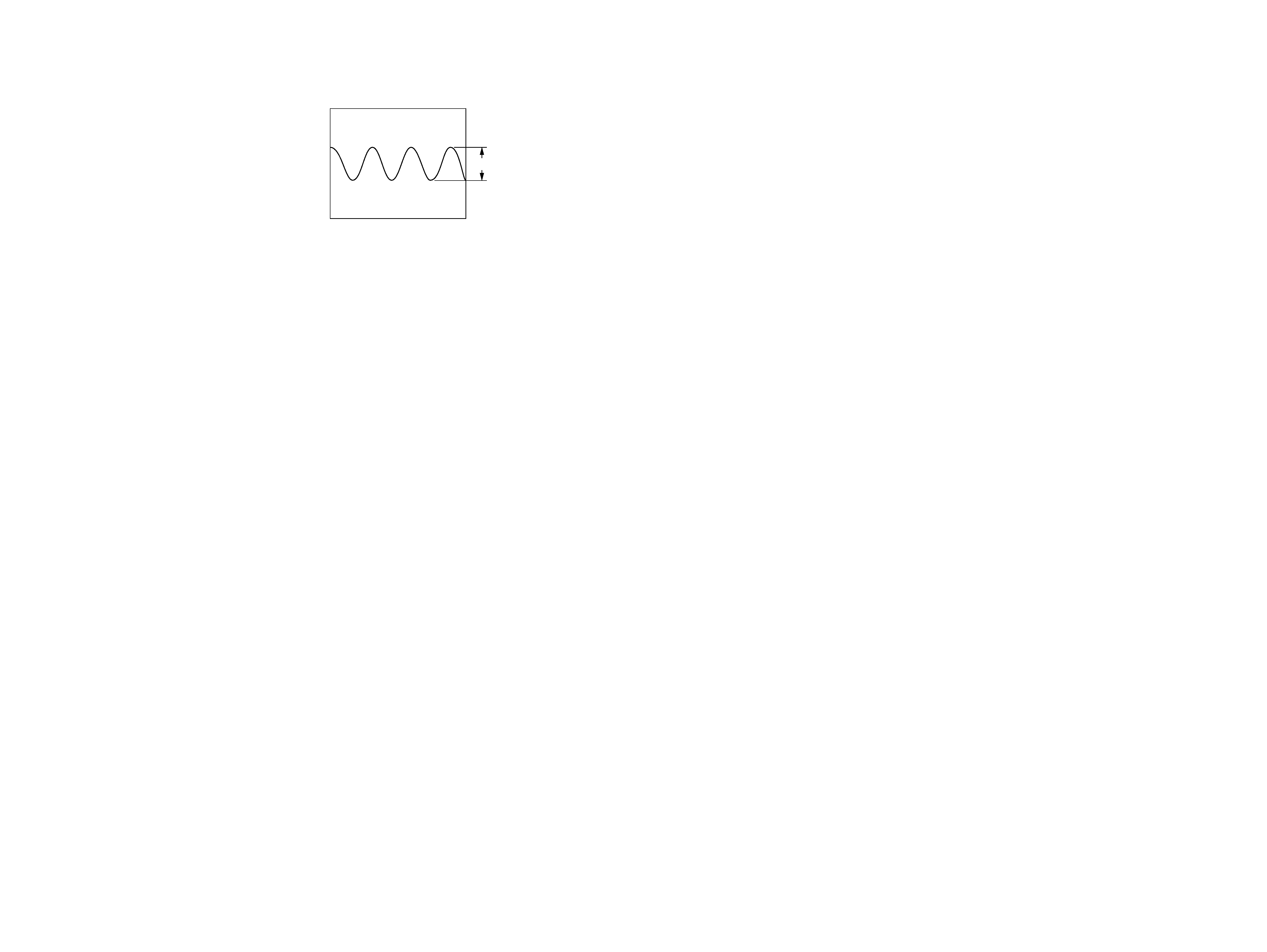
8
2.9 Vp-p
9.6 MHz
· Waveform
1 IC501 (¶ (XTALI)
Note:
· All capacitors are in µF unless otherwise noted. pF: µµF 50
WV or less are not indicated except for electrolytics and
tantalums.
· All resistors are in and 1/4 W or less unless otherwise
specified.
· C : panel designation.
· U : B+ Line.
· Power voltage is dc 3.6 V and fed with regulated dc power
supply from external power voltage jack (CN301).
· Voltages and waveforms are dc with respect to ground un-
der no-signal conditions.
no mark : Talk
· Voltages are taken with a VOM (Input impedance 10 M).
Voltage variations may be noted due to normal production
tolerances.
· Waveforms are taken with a oscilloscope.
Voltage variations may be noted due to normal production
tolerances.
· Circled numbers refer to waveforms.
· Signal path.
N : RX
O : TX
P : bell
SPP-SS961
11
12
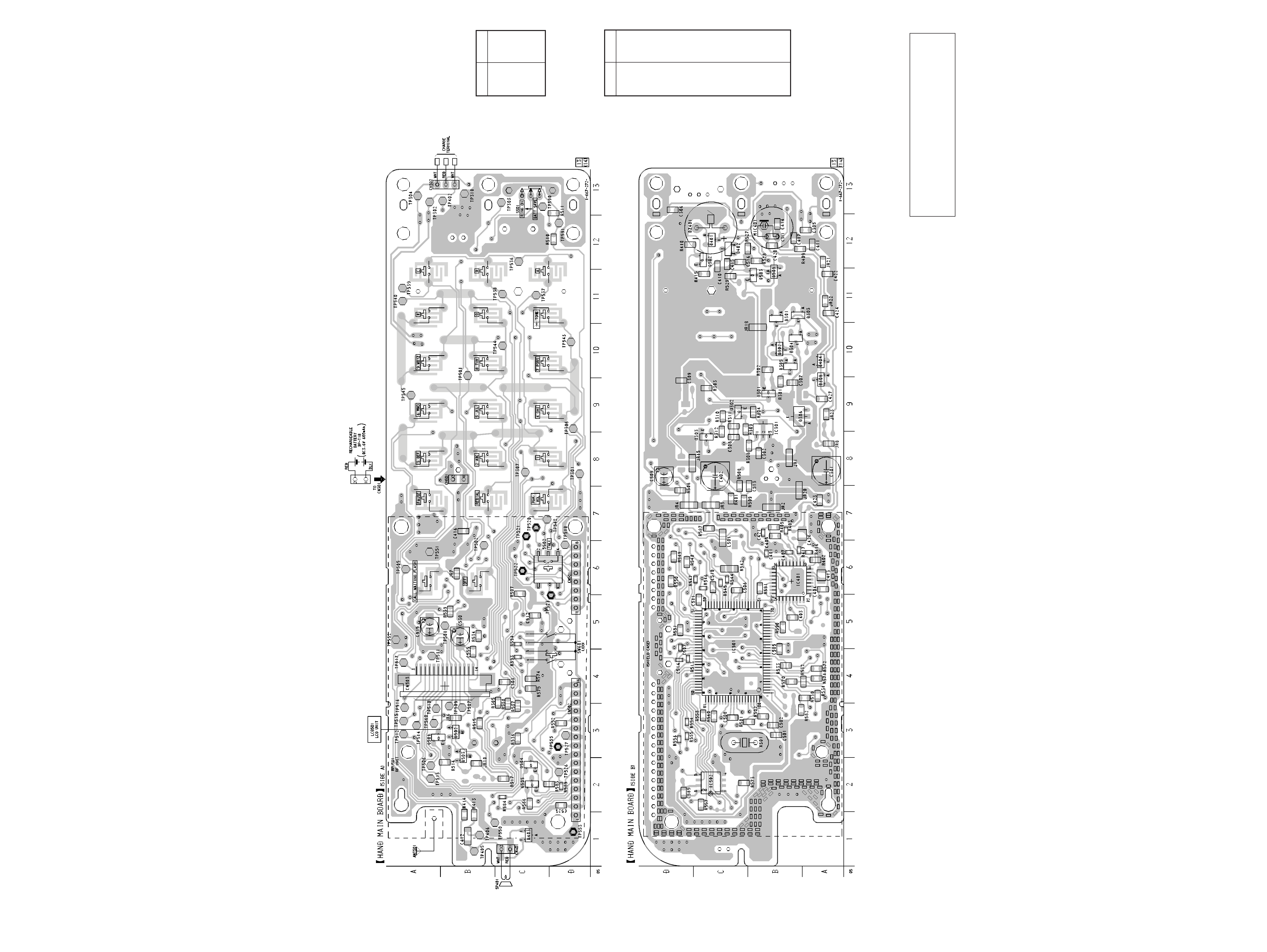
1-4.
PRINTED WIRING BOARD HANDSET Section
· Semiconductor
Location
HAND MAIN Board
(Side A)
D403
C-1
D502
B-3
D503
B-3
Q501
A-3
Q504
C-2
Q505
C-2
Caution:
Pattern face side: Parts on the pattern face side seen from the
(Side B)
pattern face are indicated.
Parts face side:
Parts on the parts face side seen from the
(Side A)
parts face are indicated.
Note:
· X : parts extracted from the component side.
· b : Pattern from the side which enables seeing.
· b : Pattern on the side which is seen. (Carbon pattern).
(The other layers' patterns are not indicated.)
Ref. No.
Location
· Semiconductor
Location
HAND MAIN Board
(Side B)
D301
B-11
D302
B-10
D303
A-11
D304
A-10
D305
A-10
D306
A-9
D308
A-9
D401
C-12
D402
C-12
D404
A-10
D505
B-11
IC301
B-9
IC401
A-6
IC501
C-4
IC502
C-2
Q301
B-9
Q302
B-9
Q303
C-8
Q502
C-12
Q503
B-11
Ref. No.
Location